EP1580842B1 - Unsymmetrische Antenne - Google Patents
Unsymmetrische Antenne Download PDFInfo
- Publication number
- EP1580842B1 EP1580842B1 EP05014460A EP05014460A EP1580842B1 EP 1580842 B1 EP1580842 B1 EP 1580842B1 EP 05014460 A EP05014460 A EP 05014460A EP 05014460 A EP05014460 A EP 05014460A EP 1580842 B1 EP1580842 B1 EP 1580842B1
- Authority
- EP
- European Patent Office
- Prior art keywords
- electrode
- ground
- dielectric substrate
- radiation
- transmission
- Prior art date
- Legal status (The legal status is an assumption and is not a legal conclusion. Google has not performed a legal analysis and makes no representation as to the accuracy of the status listed.)
- Expired - Lifetime
Links
Images







Classifications
-
- H—ELECTRICITY
- H01—ELECTRIC ELEMENTS
- H01Q—ANTENNAS, i.e. RADIO AERIALS
- H01Q1/00—Details of, or arrangements associated with, antennas
- H01Q1/36—Structural form of radiating elements, e.g. cone, spiral, umbrella; Particular materials used therewith
- H01Q1/38—Structural form of radiating elements, e.g. cone, spiral, umbrella; Particular materials used therewith formed by a conductive layer on an insulating support
-
- H—ELECTRICITY
- H01—ELECTRIC ELEMENTS
- H01Q—ANTENNAS, i.e. RADIO AERIALS
- H01Q1/00—Details of, or arrangements associated with, antennas
- H01Q1/12—Supports; Mounting means
- H01Q1/22—Supports; Mounting means by structural association with other equipment or articles
- H01Q1/24—Supports; Mounting means by structural association with other equipment or articles with receiving set
- H01Q1/241—Supports; Mounting means by structural association with other equipment or articles with receiving set used in mobile communications, e.g. GSM
- H01Q1/242—Supports; Mounting means by structural association with other equipment or articles with receiving set used in mobile communications, e.g. GSM specially adapted for hand-held use
- H01Q1/243—Supports; Mounting means by structural association with other equipment or articles with receiving set used in mobile communications, e.g. GSM specially adapted for hand-held use with built-in antennas
-
- H—ELECTRICITY
- H01—ELECTRIC ELEMENTS
- H01Q—ANTENNAS, i.e. RADIO AERIALS
- H01Q1/00—Details of, or arrangements associated with, antennas
- H01Q1/48—Earthing means; Earth screens; Counterpoises
-
- H—ELECTRICITY
- H01—ELECTRIC ELEMENTS
- H01Q—ANTENNAS, i.e. RADIO AERIALS
- H01Q17/00—Devices for absorbing waves radiated from an antenna; Combinations of such devices with active antenna elements or systems
- H01Q17/001—Devices for absorbing waves radiated from an antenna; Combinations of such devices with active antenna elements or systems for modifying the directional characteristic of an aerial
-
- H—ELECTRICITY
- H01—ELECTRIC ELEMENTS
- H01Q—ANTENNAS, i.e. RADIO AERIALS
- H01Q9/00—Electrically-short antennas having dimensions not more than twice the operating wavelength and consisting of conductive active radiating elements
- H01Q9/04—Resonant antennas
- H01Q9/0407—Substantially flat resonant element parallel to ground plane, e.g. patch antenna
-
- H—ELECTRICITY
- H01—ELECTRIC ELEMENTS
- H01Q—ANTENNAS, i.e. RADIO AERIALS
- H01Q9/00—Electrically-short antennas having dimensions not more than twice the operating wavelength and consisting of conductive active radiating elements
- H01Q9/04—Resonant antennas
- H01Q9/30—Resonant antennas with feed to end of elongated active element, e.g. unipole
-
- H—ELECTRICITY
- H01—ELECTRIC ELEMENTS
- H01Q—ANTENNAS, i.e. RADIO AERIALS
- H01Q9/00—Electrically-short antennas having dimensions not more than twice the operating wavelength and consisting of conductive active radiating elements
- H01Q9/04—Resonant antennas
- H01Q9/30—Resonant antennas with feed to end of elongated active element, e.g. unipole
- H01Q9/32—Vertical arrangement of element
- H01Q9/38—Vertical arrangement of element with counterpoise
-
- H—ELECTRICITY
- H01—ELECTRIC ELEMENTS
- H01Q—ANTENNAS, i.e. RADIO AERIALS
- H01Q9/00—Electrically-short antennas having dimensions not more than twice the operating wavelength and consisting of conductive active radiating elements
- H01Q9/04—Resonant antennas
- H01Q9/30—Resonant antennas with feed to end of elongated active element, e.g. unipole
- H01Q9/40—Element having extended radiating surface
Definitions
- the present invention relates to an antenna used for wireless communications including a wireless LAN or the like, and particularly relates to an unbalanced antenna having a radiation electrode and a ground electrode that are provided with a predetermined gap therebetween.
- the present invention relates to an unbalanced antenna that can be mounted on a small wireless communications device, and particularly relates to an unbalanced antenna that has a ground electrode reduced in size and that maintains a predetermined antenna characteristic.
- PAN personal area networks
- the unbalanced antennas In the case of the wireless communications using the wireless LAN or the like, information is transmitted via an antenna.
- the unbalanced antennas have a radiation conductor and a ground conductor that are provided with a predetermined gap therebetween. An electric signal is fed to the gap. In general, the electric signal is fed from the rear side of the ground conductor. In this case, a hole is bored in the ground conductor and the radiation conductor is extended toward the rear side.
- Example shapes of the radiation conductor are shown in Fig. 1 illustrating a monopole antenna, Fig. 2 illustrating a helical antenna, Fig. 3 illustrating a plate-like monopole antenna, and Fig. 4 illustrating a monoconical antenna.
- the unbalanced antenna can be directly connected to a coaxial transmission line used as a line for feeding an electric signal.
- the coaxial transmission line is highly resistant to an external noise. That is to say, a coaxial cable basically functions as an unbalance cable that can function in keeping with the unbalanced antenna.
- a balance-to-unbalance converter is needed between the balance antenna and the coaxial cable.
- the ground conductor can be used with a case ground conductor of the device or provided so as to be in intimate contact therewith, the device can be downsized, which is advantageous for mounting.
- the ground conductor has a disk shape measuring at least a half wave or so in diameter.
- a significantly small ground conductor deteriorates its reception characteristic or the like, thereby affecting the operation of the antenna.
- Fig. 6 illustrates the calculation result of a characteristic of the disk monopole antenna having the disk-like ground conductor measuring a half wave in diameter.
- the VSWR (Voltage Standing Wave Ratio) characteristic is shown on the left side
- the radiation directivity in a vertical surface at 3 GHz is shown in the middle
- the surface-current density distribution also at 3 GHz is shown on the right side.
- the VSWR value of about 2 or less is achieved over the range from 3.5 to 9 GHz. That is to say, a suitable impedance matching characteristic can be obtained over an ultra-wide band. Further, since the radiation directivity in the vertical surface at 3 GHz forms an 8-shape having peaks substantially along a horizontal direction, this disk monopole antenna has a characteristic similar to the inherent characteristic thereof (In a floor-limit frequency band, this antenna has a characteristic same as that of a dipole antenna.).
- the level of an unnecessary leakage current flowing on an external conductor of the coaxial transmission line is low (Where the ground conductor has an infinite width, no leakage currents flow on the external conductor of the feed transmission line on the rear side.). Therefore, this calculation result of the radiation directivity is acceptable.
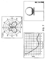
- Fig. 7 illustrates the calculation result of a characteristic of the disk monopole antenna, where the ground conductor is reduced in size.
- the VSWR characteristic is shown on the left side
- the radiation directivity in a vertical surface is shown in the middle
- the surface-current density distribution is shown on the right side.
- a comparison between the characteristic shown in Fig. 7 and that shown in Fig. 6 shows a deterioration of the impedance-matching characteristic.
- the VSWR at from 3.5 to 9 GHz increases up to 3.
- the radiation directivity in the vertical surface at 3 GHz points downward in the extreme and drops to around -10 dBi in a horizontal direction.
- the document DE 196 47 648 discloses a monopole antenna according to the preamble of claim 1.
- the document US 6 014 114 discloses an antenna having a physically small ground plane. Though physically small, the ground plane simulates an infinite ground plane. This is achieved using a plurality of resistive layers.
- An object of the invention is to provide an unbalanced antenna according to claim 1.
- the inventors divided the operation of a ground conductor of an unbalanced antenna into the following three points, including:
- the operation of the ground conductor is centralized to (a).
- the operation (a) is used only for electromagnetic-field components contributed to radiation directivity and separated from the operations (b) and (c).
- the operation (a) can be directly referred to as an "operation for forming substantially normal current distribution on the radiation conductor (original distribution obtained where the ground is unlimited)".
- the part opposed to the radiation conductor should be left, as a minimum requirement.
- the impedance variation due to the size reduction of the ground conductor that is, a change in the voltage-and-current ratio in a feed section may be compensated by mounting a suitable resistance component on the ground conductor. That is to say, for maintaining the operation (b), a part of the reduced ground conductor, the part being.near an end at a predetermined distance from the feed section, includes a conductor having low conductivity.
- the mode matching described in (c) is achieved on the precondition that feeding is performed via a coaxial transmission line. Where the ground conductor is significantly reduced, mode mismatch inevitably occurs. However, on the above-described precondition, all unnecessary unbalance components flow on an external conductor of the coaxial transmission line (referred to as a leakage current) without entering the coaxial transmission line. Subsequently, where a system for forcefully blocking the leakage current is provided, for securing the operation (c), by covering at least a single part of the external conductor of the coaxial feed line connected to the feed unit by using a current absorber, for example, it may be possible to compensate for the mode mismatch.
- a leakage current an external conductor of the coaxial transmission line
- the VSWR characteristic shown in the left part of this drawing can be compensated by mounting the resistance component. Further, the leakage-current blocking system reduces the radiation-directivity disturbance shown in the middle of this drawing.
- Fig. 8 schematically illustrates the configuration of an unbalanced antenna according to an a non claimed example.
- This drawing shows a disk monopole antenna, as an example unbalanced antenna.
- the disk monopole antenna shown in Fig. 8 includes a disk-like radiation conductor and a rectangular-plate-like ground conductor that are formed with a predetermined gap therebetween.
- the size of the ground conductor is limited, so as to correspond to a part substantially opposite to the radiation conductor.
- a part near an end of the ground conductor, the end being provided at a predetermined distance from a feed section, is formed by using a conductor with lower conductivity.
- An electric signal is fed through the coaxial transmission line from the rear side of the ground conductor.
- the coaxial transmission line is finally connected to the gap.
- Fig. 9 illustrates the calculation result of the antenna characteristic of the monopole antenna shown in Fig. 8 .
- the VSWR characteristic indicating an impedance matching characteristic is shown on the left side of this drawing, the radiation directivity in a vertical surface at 3 GHz is shown in the middle, and the surface-current density distribution also at 3 GHz (the density is shown by concentration) is shown on the right side of this drawing.
- the dimensions of the radiation conductor and the ground conductor are the same as those (the right side) of Fig. 5 .
- the conductivity of parts starting at both ends of the ground conductor and extending for 6.4 mm is determined to be 8 S/m.
- the impedance matching characteristic is apparently improved, when it is compared to the VSWR (Voltage Standing Wave Ratio) characteristic shown in Fig. 7 .
- the VSWR value is about 2 or less over the range where the frequency is at from 3.5 to 9 GHz. That is to say, the impedance matching characteristic recovers, so as to reach the level of inherent characteristic of the disk monopole antenna shown in Fig. 6 . Subsequently, the matching loss decreases and the signal distortion due to a reflected wave reduces.
- the radiation directivity in the vertical surface at 3 GHz is not improved, when it is compared to Fig. 7 .
- the radiation-directivity disturbance as such can be reduced by improving the manner of wiring the feed line.
- the feed line may be provided, so as to be orthogonal (or horizontal) to the radiation conductor. All contributions from the leakage current are converted into horizontal polarization components and not mixed with vertical polarization components from the radiation conductor. That is to say, even though radiation power distributes, the form of the vertical-polarization radiation directivity is maintained in its inherent state.
- Fig. 10 illustrates the configuration of an unbalanced antenna according to another non claimed example.
- This drawing also shows the disk monopole antenna as an example of the unbalanced antenna.
- the disk monopole antenna shown in this drawing has a disk-like radiation conductor and a rectangular-plate-like ground conductor that are provided with a predetermined gap therebetween.
- the size of the ground conductor is limited, so as to correspond to a part substantially opposite to the radiation conductor.
- parts near ends of the ground conductor, the ends being provided at a predetermined distance from a feed section, are formed by using conductors with lower conductivity.
- An electric signal is fed through a coaxial transmission line from the rear side of the ground conductor. The coaxial transmission line is finally connected to the gap.
- a part of an external conductor of the coaxial transmission line is covered by a current absorber.
- An insulator including a suitable amount of conductive material, that is, an electrical resistor is used as the current absorber.
- the use of an electric resistor with high magnetic permeability allows for reducing the length and thickness of the part to be covered, which is suitable for achieving a reduced configuration.
- the position of the part to be covered may preferably be very close to the feed-section side (gap side).
- Fig. 11 illustrates the calculation result of the antenna characteristic of the disk monopole antenna shown in Fig. 10 .
- the VSWR characteristic indicating an impedance matching characteristic is shown on the left side of this drawing, the radiation directivity in a vertical surface is shown in the middle of the drawing, and the surface-current density distribution (the density is shown by concentration) is shown on the right side of this drawing.
- the calculation conditions are the same as those of the calculations shown in Fig. 9 .
- a current absorber having predetermined electrical constants including a conductivity of 0.1 S/m and an electrical constant, that is, a relative magnetic permeability of 400 is provided immediately below the ground conductor.
- the current absorber is 3.2 mm in length, 1.6 mm in thickness, and is used as a covering.
- the impedance matching characteristic and even the disturbance in the radiation directivity are improved.
- the radiation power is slightly reduced, an inherent eight-figured characteristic having peaks along a horizontal direction is obtained.
- the level of an unnecessary leakage current flowing on the external conductor of the coaxial transmission line is low. Therefore, the radiation-directivity result is acceptable. That is to say, according to the unbalanced antenna of the example shown in Fig. 10 , an inherent and stable radiation directivity can be expected irrespective of the wiring of the feed line.
- the entire ground conductor may be formed as a conductivity-distribution ground conductor. That is to say, the conductivity of the part near the feed section is set to a high level, and the conductivity of parts near the ends is set to a low level so that the conductivity of the ground conductor changes continuously or in stages.
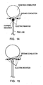
- Fig. 13 illustrates the configuration of an unbalanced antenna according to another non claimed example.
- a ground conductor is reduced in size except a part substantially opposite to a radiation conductor instead of setting the conductivity of a predetermined part of the ground conductor to a low level. Further, the ground conductor is divided into a plurality of parts according to the distance between a feed section and the ground conductor. Current resistors are connected between the divided ground conductors. This example can also obtain an effect that is the same as that of the unbalanced antenna according to the example described with reference to Fig. 8 .
- a predetermined part of an external conductor of a coaxial transmission line connected to the feed section of this unbalanced antenna may be covered by a current absorber.
- a current absorber In this case, as in the example shown in Fig. 10 , an inherent radiation-directivity characteristic can be expected irrespective of the wiring of the feed line.
- the ground conductor is reduced in size except a part substantially opposite to the radiation conductor and divided into a plurality of parts according to the distance between the feed section and the ground conductor, as shown in Fig. 15 .
- a current resistor having suitable resistivity may be respectively provided between the divided ground conductors (e.g., a current resistor having low resistivity is provided near the feed section and a current resistor having high resistivity is provided at the end).
- the mode mismatch is compensated by covering the external conductor of the coaxial transmission line by using the current absorber having the insulator including the suitable amount of conductor, that is, the electric resistor.
- a current blocking system such as a blocking ceramic tube (Sperrtopf tube) may be provided instead of using the current absorber, as shown in Fig. 16 .
- a wide-band blocking system such as the current absorber is unnecessary.
- the wide-band unbalanced antenna such as the disk monopole antenna can be effectively used as a system for correcting radiation directivity at a predetermined frequency.
- the disk monopole antenna, or the monopole antenna has been described, as an example.
- the unbalanced antenna includes a widely available dielectric substrate.
- a double-sided copper-clad dielectric substrate that is, a so-called single-layered dielectric substrate is used.
- a plate-like radiation electrode and a strip-like (narrow-plate-like) transmission-line electrode connected thereto are provided on one of surfaces of the dielectric substrate.
- the radiation electrode has a shape including a semicircle combined with a right isosceles triangle, for example.
- the disk monopole antenna is formed in free space, slight adjustment of the feed gap easily achieves impedance matching.
- a circular disk monopole antenna is formed on an electrode provided on a so-called dielectric substrate, the inventors perceived that there are limitations for the matching adjustment.
- the inventors further perceived that the above-described shape including the semicircle combined with the right isosceles triangle is suitable, where the most widely available glass-epoxy substrate (with a relative permittivity ⁇ of 4 to 5) is used.
- a ground electrode is provided on the other surface of the single-layered dielectric substrate, so as to be near a part facing the transmission-line electrode.
- the ground electrode and the transmission-line electrode together form a so-called micro-strip line.
- two sub-ground electrodes are provided on both sides of the ground electrode, so as to be adjacent thereto.
- the breadth of the entire ground electrode including the sub-ground electrodes is determined to be almost the same as that of the radiation electrode, thereby maintaining the function of serving as a pole opposed to the radiation electrode.
- electric resistors are connected between the ground electrode and the sub-ground electrodes.
- Chip-type resistors are used as the electric resistors, for example.
- An electrical signal is fed between the transmission-line electrode and the ground electrode.
- the unbalanced antenna provided on the single-layered dielectric substrate has the reduced ground electrode, it can obtain a fine impedance-matching characteristic, as is the case with Fig. 8 .
- Fig. 18 specifically illustrates a method for mounting the unbalanced antenna shown in Fig. 8 .
- the unbalanced antenna of the illustrated example includes the widely available dielectric substrate.
- two sub-ground electrodes are provided on both sides of the ground electrode, so as to be adjacent thereto.
- the breadth of the entire ground electrode including the sub-ground electrodes is determined to be almost the same as that of the radiation electrode, whereby the function of serving as a pole opposed to the radiation electrode is maintained.
- electric resistors are connected between the ground electrode and the sub-ground electrodes.
- the chip-type resistors are used as the electric resistors, for example.
- An electrical signal is fed between the transmission-line electrode and the ground electrode.
- the unbalanced antenna includes the electrodes centralized on either side of the single-layered dielectric substrate, as shown in Fig. 18 , it becomes possible to obtain a fine impedance-matching characteristic, even though the ground electrode is reduced in size.
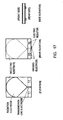
- Fig. 19 illustrates another mounting method, where an unbalanced antenna including a dielectric substrate is used.
- This embodiment shown in this drawing is different from those described with reference to Figs. 17 and 18 in that the unbalanced antenna is formed by using a multi-layered dielectric substrate.
- a multi-layered dielectric substrate having three layers, that is, upper, middle, and lower layers.
- the configurations of the intermediate-layer surface and the lower-layer surface are the same as those of the specific example shown in Fig. 17 , where the single-layered dielectric substrate is used. That is to say, a plate-like radiation electrode and a strip-like (narrow-plate like) transmission-line electrode connected to this radiation electrode are provided on the intermediate-layer surface.
- the radiation electrode has a shape having a semicircle combined with a right isosceles triangle, for example, as shown in the drawing.
- a ground electrode is provided near a part of the lower-layer surface, the part being opposed to the transmission-line electrode. Further, two sub-ground electrodes are provided on both sides of the ground electrode, so as to be adjacent thereto. The breadth of the entire ground electrode including the sub-ground electrodes is determined to be almost the same as that of the radiation electrode, whereby the function of serving as a pole opposed to the radiation electrode is maintained.
- Electric resistors are connected between the ground electrode and the sub-ground electrodes. The chip-type resistors are used, as the electric resistors, for example.
- An opposed ground electrode is provided near a part of the upper-layer surface, the part being opposed to the transmission-line electrode. Further, a plurality of through via holes is provided on both sides of the transmission-line electrode on the intermediate-layer surface, so as to sandwich the transmission-line electrode. Subsequently, the ground electrode on the lower-layer surface is electrically connected to the opposed ground electrode on the upper-layer surface.
- An electrical signal is fed between the transmission-line electrode and the ground electrodes, or the transmission-line electrode and the opposed ground electrode.
- Fig. 20 illustrates another mounting example, where an unbalanced antenna is formed by using a multi-layered dielectric substrate having three electrode layers, that is, upper, intermediate, and lower layers.
- a current absorber is added to the mounting example shown in Fig. 19 , so as to cover a part of a periphery of a ground electrode and an opposed ground electrode. More preferably, the current absorber covers the part of the periphery of the ground electrode and the opposed ground electrode, so as to be in intimate contact therewith.
- a fine impedance-matching characteristic can be obtained, even though the ground conductor is reduced in size. Further, it becomes possible to expect a stable radiation directivity specific to the unbalanced antenna irrespective of the wiring of the feed line,
- the main point of the present invention is not limited to the shapes shown in the drawings. Further, a large number of the sub-ground electrodes may be provided end to end, so as to be adjacent to one another.
- Fig. 21 illustrates a specific mounting example, where an insulator body such as a widely available engineering plastic is used for forming the unbalanced antenna according to a non claimed example.
- a cone-shaped indentation is provided on one of end faces of the insulator and a radiation electrode is formed on the surface of the inside of the indentation by a plating method or the like. Otherwise, the radiation electrode may be formed, so as to fill the entire indentation.
- the radiation electrode is extended from the apex of the indentation, so as to reach the other end face opposed to the end face of the insulator, and a ground electrode is provided on the other end face, so as to enclose the extended radiation electrode.
- the size of the ground electrode is determined to be almost the same as that of the base of the indentation, so as to maintain the function of serving as a pole opposed to the radiation electrode.
- a peripheral part of the ground electrode is peeled off and a predetermined exposed part of the insulator is bored. Then, an electric resistor is embedded in the bored part.
- the electric resistor may be formed by using rubber or elastomer including a suitable amount of conductor. An electric signal is fed between the extended radiation electrode and the ground electrode.
- the shape of the indentation provided in the insulator body is not limited to the cone shape shown in Fig. 21 .
- it may be an elliptic cone, or a pyramid.
- the outside shape of the insulator body is not limited. Basically, the outside shape may be anything having two opposing end faces, such as a cylinder or a prism.
- the number of the peeled and bored peripheral part formed on the ground electrode on the base is not limited to one, but can be two or more. Further, as shown in the drawing, a step may be deliberately provided on the surface of the ground electrode, so as to be easily mounted on the substrate.
- the present invention allows for significantly reducing a ground conductor of an unbalanced antenna of any kind, while reducing a significant deterioration of the impedance-matching characteristic and radiation directivity of the unbalanced antenna. Further, the present invention can make almost full use of the capabilities of an unbalanced antenna, where the unbalanced antenna is mounted on a rather small unwired communications device.
- the present invention can be effectively used for an unbalanced antenna for a very wide frequency band. Therefore, the present invention is suitable for downsizing an antenna of an ultra-wide-band communications system.
Landscapes
- Engineering & Computer Science (AREA)
- Computer Networks & Wireless Communication (AREA)
- Details Of Aerials (AREA)
- Waveguide Aerials (AREA)
- Elimination Of Static Electricity (AREA)
Claims (8)
- Unsymmetrische Antenne, die umfasst:ein einlagiges oder mehrlagiges dielektrische Substrat, das mindestens zwei Elektrodenflächen besitzt;eine plattenartige Strahlungs-Elektrode und eine, an die Strahlungs-Elektrode angeschlossene, Übertragungsleitungs-Elektrode, die auf einer der Flächen des dielektrischen Substrats ausgebildet sind.eine Ground-Elektrode, die auf einem vorbestimmten Teil nahe der Übertragungsleitungs-Elektrode ausgebildet ist, wobei die Ground-Elektrode auf der Fläche des dielektrischen Substrats angeordnet ist, auf der die plattenartige Strahlungs-Elektrode und die Übertragungsleitungs-Elektrode ausgebildet sind;mindestens eine Sub-Ground-Elektrode, die auf der selben Fläche des dielektrischen Substrats bereitgestellt ist wie die Ground-Elektrode, so dass sie an die Ground-Elektrode grenzt, wobei die Breite der gesamten Ground-Elektrode inklusive der Sub-Ground-Elektrode so festgelegt ist, dass sie im Wesentlichen die selbe wie die der Strahlungs-Elektrode ist;einen elektrischen Widerstand, der zwischen die Ground-Elektrode und die Sub-Ground-Elektrode angeschlossen ist; undeine Zuführbahn für ein elektrisches Signal, die zwischen der Übertragungsleitungs-Elektrode und der Ground-Elektrode bereitgestellt ist.
- Unsymmetrische Antenne aus Anspruch 1,
wobei das dielektrische Substrat ein einlagiges Substrat ist, das zwei Elektrodenflächen besitzt, und zwar Oberlagen- und Unterlagen-Elektrodenflächen;
wobei die plattenartige Strahlungs-Elektrode und die Übertragungsleitungs-Elektrode auf einer Fläche des einlagigen dielektrischen Substrats ausgebildet sind;
und wobei die Ground-Elektrode nahe eines vorbestimmten Teils der anderen Fläche des einlagigen dielektrischen Substrats ausgebildet ist, wobei das vorbestimmte Teil gegenüber der Übertragungsleitungs-Elektrode liegt. - Unsymmetrische Antenne aus Anspruch 1,
wobei das dielektrische Substrat ein mehrlagiges dielektrisches Substrat ist, das drei Elektrodenflächen besitzt, und zwar Oberlagen-, Zwischenlagen- und Unterlagen-Elektrodenflächen;
wobei die plattenartige Strahlungs-Elektrode und die Übertragungsleitungs-Elektrode an die Strahlungs-Elektrode angeschlossen sind, die auf der Zwischenlagenfläche des mehrlagigen dielektrischen Substrats ausgebildet ist;
wobei die Ground-Elektrode nahe eines vorbestimmten Teils der Unterlagenfläche des mehrlagigen dielektrischen Substrats ausgebildet ist, wobei der vorbestimmte Teil gegenüber der Übertragungsleitungs-Elektrode liegt;
wobei die unsymmetrische Antenne weiterhin umfasst:eine gegenüberliegende Ground-Elektrode, die nahe eines vorbestimmten Teils der Oberlagenfläche des mehrlagigen dielektrischen Substrats ausgebildet ist, wobei der vorbestimmte Teil gegenüber der Übertragungsleitungs-Elektrode liegt;zwei oder mehr Inter-Ground-Elektroden Verbindungsabschnitte zum elektrischen Verbinden der Ground-Elektrode mit der gegenüberliegenden Ground-Elektrode;und wobei die Zuführbahn für ein elektrisches Signal zwischen der Übertragungsleitungs-Elektrode und der Ground-Elektrode, und/oder der Übertragungsleitungs-Elektrode und der gegenüberliegenden Ground-Elektorde ausgebildet ist. - Unsymmetrische Antenne gemäß Anspruch 3, wobei die Inter-Ground-Elektroden Verbindungsabschnitte auf beiden Seiten der Übertragungsleitungs-Elektrode bereitgestellt sind, die auf der Zwischenlagenfläche bereitgestellt ist, so dass sie die Übertragungsleitungs-Elektrode einschließen.
- Unsymmetrische Antenne gemäß Anspruch 3 oder 4, die weiterhin umfasst:einen Stromabsorber der einen vorbestimmten Teil eines Umfangs der Gound-Elektrode und der gegenüberliegenden Ground-Elektrode bedeckt.
- Unsymmetrische Antenne gemäß einem der Ansprüche 1 bis 5,
wobei der elektrische Widerstand ausgebildet ist, indem ein chipartiger Widerstand benutzt wird. - Unsymmetrische Antenne gemäß einem der Ansprüche 1 bis 6,
wobei mehrere der Sub-Ground-Elektroden End-zu-End bereitgestellt sind, so dass sie aneinander grenzen. - Unsymmetrische Antenne, gemäß einem der Ansprüche 1 bis 7,
wobei die Strahlungs-Elektrode eine Form hat, die einen Halbkreis kombiniert mit einem rechts gleichschenkeligen Dreieck enthält.
Applications Claiming Priority (3)
| Application Number | Priority Date | Filing Date | Title |
|---|---|---|---|
| JP2002307910 | 2002-10-23 | ||
| JP2002307910A JP3620044B2 (ja) | 2002-10-23 | 2002-10-23 | 不平衡型アンテナ |
| EP03754132A EP1564841A4 (de) | 2002-10-23 | 2003-10-15 | Unsymmetrische antenne |
Related Parent Applications (2)
| Application Number | Title | Priority Date | Filing Date |
|---|---|---|---|
| EP03754132A Division EP1564841A4 (de) | 2002-10-23 | 2003-10-15 | Unsymmetrische antenne |
| EP03754132.3 Division | 2003-10-15 |
Publications (3)
| Publication Number | Publication Date |
|---|---|
| EP1580842A2 EP1580842A2 (de) | 2005-09-28 |
| EP1580842A3 EP1580842A3 (de) | 2006-05-10 |
| EP1580842B1 true EP1580842B1 (de) | 2009-09-02 |
Family
ID=32170952
Family Applications (2)
| Application Number | Title | Priority Date | Filing Date |
|---|---|---|---|
| EP03754132A Withdrawn EP1564841A4 (de) | 2002-10-23 | 2003-10-15 | Unsymmetrische antenne |
| EP05014460A Expired - Lifetime EP1580842B1 (de) | 2002-10-23 | 2003-10-15 | Unsymmetrische Antenne |
Family Applications Before (1)
| Application Number | Title | Priority Date | Filing Date |
|---|---|---|---|
| EP03754132A Withdrawn EP1564841A4 (de) | 2002-10-23 | 2003-10-15 | Unsymmetrische antenne |
Country Status (9)
| Country | Link |
|---|---|
| US (2) | US7180466B2 (de) |
| EP (2) | EP1564841A4 (de) |
| JP (1) | JP3620044B2 (de) |
| KR (1) | KR101077792B1 (de) |
| CN (1) | CN100483847C (de) |
| AU (1) | AU2003273012A1 (de) |
| BR (1) | BR0306600A (de) |
| DE (1) | DE60329125D1 (de) |
| WO (1) | WO2004038860A1 (de) |
Families Citing this family (20)
| Publication number | Priority date | Publication date | Assignee | Title |
|---|---|---|---|---|
| JP2005094437A (ja) * | 2003-09-18 | 2005-04-07 | Mitsumi Electric Co Ltd | Uwb用アンテナ |
| JP3964382B2 (ja) * | 2003-11-11 | 2007-08-22 | ミツミ電機株式会社 | アンテナ装置 |
| JP2005269366A (ja) * | 2004-03-19 | 2005-09-29 | Mitsubishi Electric Corp | アンテナ装置 |
| CN1330052C (zh) * | 2005-06-15 | 2007-08-01 | 东南大学 | 延迟线电阻加载脉冲天线 |
| GB2439110B (en) * | 2006-06-13 | 2009-08-19 | Thales Holdings Uk Plc | An ultra wideband antenna |
| JP2008263384A (ja) * | 2007-04-11 | 2008-10-30 | Omron Corp | 広帯域アンテナ |
| US8564385B2 (en) * | 2007-08-23 | 2013-10-22 | Lockheed Martin Corporation | Coaxial concentric nonlinear transmission line |
| US8730114B2 (en) * | 2010-06-02 | 2014-05-20 | Mitre Corporation | Low-profile multiple-beam lens antenna |
| EP2645298A1 (de) * | 2012-03-30 | 2013-10-02 | austriamicrosystems AG | Tragbarer Gegenstand und Informationsübertragungssystem |
| US9972902B2 (en) | 2014-11-04 | 2018-05-15 | Panasonic Intellectual Property Management Co., Ltd. | Antenna device and electronic device |
| TWI563737B (en) * | 2015-05-26 | 2016-12-21 | Wistron Neweb Corp | Collinear Dipole Antenna and Communication Device Thereof |
| CN106299707B (zh) * | 2015-06-04 | 2019-04-16 | 启碁科技股份有限公司 | 共线偶极天线及相关通讯装置 |
| US11233327B2 (en) * | 2015-11-09 | 2022-01-25 | Wiser Systems, Inc. | Ultra-wideband (UWB) antennas and related enclosures for the UWB antennas |
| EP3174158A1 (de) * | 2015-11-27 | 2017-05-31 | AGC Glass Europe | Hochfrequenz- und breitbandantenne mit verbindungsüberwachungseinrichtung |
| CN106252852A (zh) * | 2016-09-18 | 2016-12-21 | 北京石油化工学院 | 单极子超宽带天线 |
| KR101750336B1 (ko) * | 2017-03-31 | 2017-06-23 | 주식회사 감마누 | 다중대역 기지국 안테나 |
| JP2019047328A (ja) * | 2017-09-01 | 2019-03-22 | 富士通株式会社 | アンテナ及び通信装置 |
| US11469502B2 (en) * | 2019-06-25 | 2022-10-11 | Viavi Solutions Inc. | Ultra-wideband mobile mount antenna apparatus having a capacitive ground structure-based matching structure |
| US11611145B2 (en) * | 2021-01-28 | 2023-03-21 | Infinidome Ltd. | Ground plane for asymmetric antenna |
| WO2026141116A1 (ja) * | 2024-12-25 | 2026-07-02 | ソニーグループ株式会社 | 通信機器、及びアンテナ装置 |
Family Cites Families (19)
| Publication number | Priority date | Publication date | Assignee | Title |
|---|---|---|---|---|
| US2237792A (en) * | 1938-05-14 | 1941-04-08 | Telefunken Gmbh | Antenna system and feeder |
| DE718695C (de) | 1938-05-14 | 1942-03-18 | Telefunken Gmbh | Abgeschirmte Antennenzuleitung |
| JPS418371B1 (de) | 1963-12-07 | 1966-04-30 | ||
| DE4205851C2 (de) * | 1992-02-26 | 1995-10-12 | Flachglas Ag | In die Fensteröffnung einer metallischen Kraftfahrzeugkarosserie einzusetzende Antennenscheibe |
| JPH08139515A (ja) | 1994-11-11 | 1996-05-31 | Toko Inc | 誘電体垂直偏波アンテナ |
| CA2212015A1 (en) | 1995-02-06 | 1996-08-15 | John R. Benham | Television antennas |
| JP3273463B2 (ja) | 1995-09-27 | 2002-04-08 | 株式会社エヌ・ティ・ティ・ドコモ | 半円形放射板を使った広帯域アンテナ装置 |
| US5847682A (en) * | 1996-09-16 | 1998-12-08 | Ke; Shyh-Yeong | Top loaded triangular printed antenna |
| US5828340A (en) | 1996-10-25 | 1998-10-27 | Johnson; J. Michael | Wideband sub-wavelength antenna |
| DE19647648C2 (de) * | 1996-11-18 | 1999-12-09 | Ind Tech Res Inst | Gedruckte Antenne mit einem Resonatorelement |
| US5990845A (en) * | 1997-07-02 | 1999-11-23 | Tci International | Broadband fan cone direction finding antenna and array |
| US6014114A (en) * | 1997-09-19 | 2000-01-11 | Trimble Navigation Limited | Antenna with stepped ground plane |
| US5986615A (en) | 1997-09-19 | 1999-11-16 | Trimble Navigation Limited | Antenna with ground plane having cutouts |
| US6307525B1 (en) * | 2000-02-25 | 2001-10-23 | Centurion Wireless Technologies, Inc. | Multiband flat panel antenna providing automatic routing between a plurality of antenna elements and an input/output port |
| IT1319430B1 (it) | 2000-09-13 | 2003-10-10 | Zendar Spa | Antenna a basso profilo, senza stilo |
| US6809687B2 (en) * | 2001-10-24 | 2004-10-26 | Alps Electric Co., Ltd. | Monopole antenna that can easily be reduced in height dimension |
| JP3964382B2 (ja) * | 2003-11-11 | 2007-08-22 | ミツミ電機株式会社 | アンテナ装置 |
| JP4280182B2 (ja) * | 2004-03-09 | 2009-06-17 | 富士通コンポーネント株式会社 | アンテナ装置 |
| TWI267230B (en) * | 2004-06-15 | 2006-11-21 | Lin Ting Yu | Ultra wide band planner volcano smoke antenna |
-
2002
- 2002-10-23 JP JP2002307910A patent/JP3620044B2/ja not_active Expired - Fee Related
-
2003
- 2003-10-15 WO PCT/JP2003/013185 patent/WO2004038860A1/ja not_active Ceased
- 2003-10-15 EP EP03754132A patent/EP1564841A4/de not_active Withdrawn
- 2003-10-15 CN CNB200380100055XA patent/CN100483847C/zh not_active Expired - Fee Related
- 2003-10-15 EP EP05014460A patent/EP1580842B1/de not_active Expired - Lifetime
- 2003-10-15 BR BR0306600-2A patent/BR0306600A/pt not_active IP Right Cessation
- 2003-10-15 AU AU2003273012A patent/AU2003273012A1/en not_active Abandoned
- 2003-10-15 US US10/498,518 patent/US7180466B2/en not_active Expired - Fee Related
- 2003-10-15 DE DE60329125T patent/DE60329125D1/de not_active Expired - Lifetime
- 2003-10-15 KR KR1020047009666A patent/KR101077792B1/ko not_active Expired - Fee Related
-
2006
- 2006-12-26 US US11/616,230 patent/US7515114B2/en not_active Expired - Fee Related
Also Published As
| Publication number | Publication date |
|---|---|
| US20070176828A1 (en) | 2007-08-02 |
| DE60329125D1 (de) | 2009-10-15 |
| EP1580842A2 (de) | 2005-09-28 |
| CN1685561A (zh) | 2005-10-19 |
| CN100483847C (zh) | 2009-04-29 |
| EP1564841A1 (de) | 2005-08-17 |
| JP3620044B2 (ja) | 2005-02-16 |
| US7180466B2 (en) | 2007-02-20 |
| BR0306600A (pt) | 2004-09-28 |
| AU2003273012A1 (en) | 2004-05-13 |
| EP1580842A3 (de) | 2006-05-10 |
| US20060214869A1 (en) | 2006-09-28 |
| KR20050071364A (ko) | 2005-07-07 |
| WO2004038860A1 (ja) | 2004-05-06 |
| EP1564841A4 (de) | 2005-12-21 |
| KR101077792B1 (ko) | 2011-10-28 |
| US7515114B2 (en) | 2009-04-07 |
| JP2004146978A (ja) | 2004-05-20 |
Similar Documents
| Publication | Publication Date | Title |
|---|---|---|
| US7180466B2 (en) | Unbalanced antenna | |
| EP1088367B1 (de) | Wendelantenne | |
| KR100836213B1 (ko) | 안테나, 무선장치, 안테나 설계 방법 및 안테나의 동작주파수 측정 방법 | |
| KR100621335B1 (ko) | 폴더타입 통신 핸드셋 장치 내에서의 접지효과 감소 장치 | |
| JPH061848B2 (ja) | アンテナ | |
| US6067052A (en) | Loop antenna configuration for printed wire board applications | |
| CN1628399A (zh) | 双波段片状蝴蝶结隙缝天线结构 | |
| US20100321273A1 (en) | Wideband antenna and clothing and articles using the same | |
| JPH08242117A (ja) | アンテナ一体型ストリップラインケーブル | |
| US7791554B2 (en) | Tulip antenna with tuning stub | |
| US20120223864A1 (en) | Multiband antenna | |
| US20080261667A1 (en) | Mobile terminal having an improved internal antenna | |
| US20050237244A1 (en) | Compact RF antenna | |
| CN101378144A (zh) | 无线电设备及其天线 | |
| US7173566B2 (en) | Low-sidelobe dual-band and broadband flat endfire antenna | |
| JPH05299929A (ja) | アンテナ | |
| KR20090061585A (ko) | 안테나 장치 | |
| US20240356209A1 (en) | Devices with Radiating Systems Proximate to Conductive Bodies | |
| JP3775422B2 (ja) | 不平衡型アンテナ | |
| US6480171B1 (en) | Impedance matching means between antenna and transmission cable | |
| JPH10200438A (ja) | 携帯無線機 | |
| KR100643543B1 (ko) | 다중 대역 모노폴 안테나 | |
| JP2002050918A (ja) | チップアンテナ | |
| JP2004173143A (ja) | アンテナと通信ケーブルの接続部構造 | |
| WO2002007255A1 (en) | Internal patch antenna for portable terminal |
Legal Events
| Date | Code | Title | Description |
|---|---|---|---|
| PUAI | Public reference made under article 153(3) epc to a published international application that has entered the european phase |
Free format text: ORIGINAL CODE: 0009012 |
|
| 17P | Request for examination filed |
Effective date: 20050704 |
|
| AC | Divisional application: reference to earlier application |
Ref document number: 1564841 Country of ref document: EP Kind code of ref document: P |
|
| AK | Designated contracting states |
Kind code of ref document: A2 Designated state(s): AT BE BG CH CY CZ DE DK EE ES FI FR GB GR HU IE IS IT LI LT LU LV MC NL PL PT RO SE SI SK TR |
|
| AX | Request for extension of the european patent |
Extension state: AL BA HR MK YU |
|
| PUAL | Search report despatched |
Free format text: ORIGINAL CODE: 0009013 |
|
| AK | Designated contracting states |
Kind code of ref document: A3 Designated state(s): AT BE BG CH CY CZ DE DK EE ES FI FR GB GR HU IE IS IT LI LT LU LV MC NL PL PT RO SE SI SK TR |
|
| AX | Request for extension of the european patent |
Extension state: AL BA HR MK YU |
|
| 17Q | First examination report despatched |
Effective date: 20060714 |
|
| AKX | Designation fees paid |
Designated state(s): DE FR GB IT |
|
| GRAP | Despatch of communication of intention to grant a patent |
Free format text: ORIGINAL CODE: EPIDOSNIGR1 |
|
| GRAS | Grant fee paid |
Free format text: ORIGINAL CODE: EPIDOSNIGR3 |
|
| GRAA | (expected) grant |
Free format text: ORIGINAL CODE: 0009210 |
|
| AC | Divisional application: reference to earlier application |
Ref document number: 1564841 Country of ref document: EP Kind code of ref document: P |
|
| AK | Designated contracting states |
Kind code of ref document: B1 Designated state(s): DE FR GB IT |
|
| REF | Corresponds to: |
Ref document number: 60329125 Country of ref document: DE Date of ref document: 20091015 Kind code of ref document: P |
|
| PLBE | No opposition filed within time limit |
Free format text: ORIGINAL CODE: 0009261 |
|
| STAA | Information on the status of an ep patent application or granted ep patent |
Free format text: STATUS: NO OPPOSITION FILED WITHIN TIME LIMIT |
|
| 26N | No opposition filed |
Effective date: 20100603 |
|
| PGFP | Annual fee paid to national office [announced via postgrant information from national office to epo] |
Ref country code: FR Payment date: 20101104 Year of fee payment: 8 |
|
| PGFP | Annual fee paid to national office [announced via postgrant information from national office to epo] |
Ref country code: DE Payment date: 20101022 Year of fee payment: 8 |
|
| PG25 | Lapsed in a contracting state [announced via postgrant information from national office to epo] |
Ref country code: IT Free format text: LAPSE BECAUSE OF FAILURE TO SUBMIT A TRANSLATION OF THE DESCRIPTION OR TO PAY THE FEE WITHIN THE PRESCRIBED TIME-LIMIT Effective date: 20090902 |
|
| PGFP | Annual fee paid to national office [announced via postgrant information from national office to epo] |
Ref country code: GB Payment date: 20101021 Year of fee payment: 8 |
|
| GBPC | Gb: european patent ceased through non-payment of renewal fee |
Effective date: 20111015 |
|
| REG | Reference to a national code |
Ref country code: FR Ref legal event code: ST Effective date: 20120629 |
|
| PG25 | Lapsed in a contracting state [announced via postgrant information from national office to epo] |
Ref country code: DE Free format text: LAPSE BECAUSE OF NON-PAYMENT OF DUE FEES Effective date: 20120501 |
|
| REG | Reference to a national code |
Ref country code: DE Ref legal event code: R119 Ref document number: 60329125 Country of ref document: DE Effective date: 20120501 |
|
| PG25 | Lapsed in a contracting state [announced via postgrant information from national office to epo] |
Ref country code: FR Free format text: LAPSE BECAUSE OF NON-PAYMENT OF DUE FEES Effective date: 20111102 Ref country code: GB Free format text: LAPSE BECAUSE OF NON-PAYMENT OF DUE FEES Effective date: 20111015 |