EP1580586B1 - Microscope confocal à balayage - Google Patents
Microscope confocal à balayage Download PDFInfo
- Publication number
- EP1580586B1 EP1580586B1 EP05006144A EP05006144A EP1580586B1 EP 1580586 B1 EP1580586 B1 EP 1580586B1 EP 05006144 A EP05006144 A EP 05006144A EP 05006144 A EP05006144 A EP 05006144A EP 1580586 B1 EP1580586 B1 EP 1580586B1
- Authority
- EP
- European Patent Office
- Prior art keywords
- light
- optical fiber
- scanning
- examination
- optical
- Prior art date
- Legal status (The legal status is an assumption and is not a legal conclusion. Google has not performed a legal analysis and makes no representation as to the accuracy of the status listed.)
- Expired - Fee Related
Links
Images


Classifications
-
- G—PHYSICS
- G02—OPTICS
- G02B—OPTICAL ELEMENTS, SYSTEMS OR APPARATUS
- G02B21/00—Microscopes
- G02B21/0004—Microscopes specially adapted for specific applications
- G02B21/002—Scanning microscopes
- G02B21/0024—Confocal scanning microscopes (CSOMs) or confocal "macroscopes"; Accessories which are not restricted to use with CSOMs, e.g. sample holders
- G02B21/0036—Scanning details, e.g. scanning stages
- G02B21/0048—Scanning details, e.g. scanning stages scanning mirrors, e.g. rotating or galvanomirrors, MEMS mirrors
-
- G—PHYSICS
- G02—OPTICS
- G02B—OPTICAL ELEMENTS, SYSTEMS OR APPARATUS
- G02B21/00—Microscopes
- G02B21/0004—Microscopes specially adapted for specific applications
- G02B21/002—Scanning microscopes
- G02B21/0024—Confocal scanning microscopes (CSOMs) or confocal "macroscopes"; Accessories which are not restricted to use with CSOMs, e.g. sample holders
- G02B21/0036—Scanning details, e.g. scanning stages
- G02B21/004—Scanning details, e.g. scanning stages fixed arrays, e.g. switchable aperture arrays
-
- G—PHYSICS
- G02—OPTICS
- G02B—OPTICAL ELEMENTS, SYSTEMS OR APPARATUS
- G02B21/00—Microscopes
- G02B21/0004—Microscopes specially adapted for specific applications
- G02B21/002—Scanning microscopes
- G02B21/0024—Confocal scanning microscopes (CSOMs) or confocal "macroscopes"; Accessories which are not restricted to use with CSOMs, e.g. sample holders
- G02B21/0052—Optical details of the image generation
- G02B21/0076—Optical details of the image generation arrangements using fluorescence or luminescence
Definitions
- the present invention relates to an optical-scanning examination apparatus.
- This optical-scanning examination apparatus includes a scanning laser microscope formed of a fluorescence microscope, an optical fiber bundle one end of which is disposed at the focal plane of a first objective lens in this scanning laser microscope, and a second objective lens disposed so that the other end of this optical fiber bundle serves as a light source therefor.
- the end of the optical fiber functions as a confocal pinhole, and fluorescence is produced at the focal position of the second objective lens by the laser light focused thereat. This allows the internal structure of a living organism to be determined.
- Japanese Unexamined Patent Application Publication No. 2003-344777 also discloses a confocal scanner in which a focusing disk and a pinhole disk are connected and rotationally driven with a motor. By using this confocal scanner, a plurality of spots are scanned on the specimen simultaneously, which enables confocal images to be acquired at high speed.
- the optical-scanning examination apparatus disclosed in Japanese Unexamined Patent Application Publication No. 2003-344777 uses a single pinhole disk including a fixed-type confocal pinhole or a predetermined pinhole pattern. Therefore, the region that can be examined is restricted to an extremely thin region in the depth direction below the surface of the living organism. As a result, this apparatus suffers from the drawback that it is difficult to detect or focus on the examination site. To overcome this drawback, a plurality of confocal pinholes or pinhole disks are prepared, and they can be replaced. However, this results in the drawback that the ease-of-use is reduced and the operation becomes cumbersome. Also, in some cases it may be preferable to obtain bright fluorescence images from deep within the object under examination, even though the resolution is low.
- Irish Patent Application Publication No. 2000-0001 describes a confocal microscope system incorporating a micro lens array for selectively focussing illumination light on individual optical fibres in an optical fibre bundle.
- An object of the present invention is to provide an optical-scanning confocal microscope apparatus having a simple configuration, in which the resolution of acquired images can be freely adjusted and in which the brightness and examination depth of fluorescence images can be adjusted according to the type of examination to be performed.
- the present invention provides an optical-scanning examination apparatus having the features recited in claim 1.
- the present invention provides an optical-scanning examination apparatus including a light source unit; a focusing lens for forming a first intermediate image of excitation light emitted from the light source unit; an imaging lens for focusing the first intermediate image; a first objective lens for forming a second intermediate image of the excitation light focused by the imaging lens; an optical fiber bundle one end face of which is disposed near the second intermediate image position; a second objective lens, disposed at the other end face of the optical fiber bundle, for imaging light emitted from the other end face of the optical fiber bundle onto a specimen; an imaging unit for imaging return light that returns via the second objective lens, the optical fiber bundle, the first objective lens, and the imaging lens; and a scanning mirror device, disposed at the first intermediate image position, the scanning mirror device being formed of a plurality of mirrors that simultaneously receive the first intermediate image and that can be selectively turned on and off.
- the excitation light emitted from the light source unit is focused with the focusing lens to form a first intermediate image. Since the scanning mirror device is disposed at the position of the first intermediate image, by selectively turning on and off the plurality of mirrors constituting the scanning mirror device, the excitation light forming the first intermediate image can be partially reflected, and can be irradiated onto the specimen via the imaging lens, the first objective lens, the optical fiber bundle, and the second objective lens. Returning light, such as fluorescence generated at the specimen, returns via the second objective lens, the optical fiber bundle, the first objective lens, and the imaging lens, and only the light reflected at the turned-on mirrors in the scanning mirror device is imaged in the imaging unit.
- each mirror constituting the scanning mirror device By sequentially switching the turned-on mirror in the mirrors constituting the scanning mirror device, the irradiation position of the excitation light on the specimen can be changed, which enables examination of wide area.
- each mirror By making each mirror constituting the scanning mirror device sufficiently small, each mirror can be made to function as a confocal pinhole, which allows confocal fluorescence images of a wide examination site at a predetermined depth below the surface of the specimen to be acquired.
- the on/off state of the mirrors in the scanning mirror device can be arbitrarily changed, it is possible to achieve an effect similar to switching between a plurality of confocal pinholes by changing the on/off state of the mirrors.
- this can be achieved by reducing the number of turned-on mirrors, and when it is desired to obtain a bright image at a certain depth, this can be achieved by turning on a plurality of adjacent mirrors.
- the optical-scanning examination apparatus may also include a control apparatus for controlling the driving pattern of each mirror constituting the scanning mirror device.
- control apparatus By operating the control apparatus to control each mirror with a predetermined driving pattern, it is possible to select a desired examination format, which allows examination that best suits the type of examination object. Also, the driving pattern can be changed easily and quickly with the control apparatus.
- the optical fiber bundle includes a plurality of fiber cores, and each mirror constituting the scanning mirror device and each fiber core constituting the optical fiber bundle are disposed in one-to-one correspondence.
- the light can propagate efficiently in both the scanning mirror device and the optical fiber bundle without restricting the resolution.
- the optical fiber bundle includes a plurality of fiber cores, and each mirror constituting the scanning mirror device and each fiber core constituting the optical fiber bundle are disposed in one-to-many or many-to-one correspondence.
- the resolution is limited by either the scanning mirror device or the optical fiber bundle; however, the confocal pinhole effect at the scanning mirror device is low, which allows bright, deep images to be acquired.
- the optical-scanning examination apparatus may also include a galvano mirror.
- the first image is formed in the shape of a line; the plurality of mirrors, which can be selectively turned on and off, in the scanning mirror device are arrayed in at least one row; and the galvano mirror scans the light reflected at the mirrors constituting the scanning mirror device in a direction orthogonal to the arrayed direction of the mirrors.
- the excitation light is scanned in one direction by driving the scanning mirror device and the excitation light is scanned in a direction perpendicular thereto by the galvano mirror, it is possible to two-dimensionally scan the excitation light on the specimen.
- the first intermediate image as a line, it is possible to focus the excitation light emitted from the light source unit into a narrower region compared to the case where a two-dimensional first intermediate image is formed.
- the resolution of acquired images can be freely adjusted with a simple configuration, which affords an advantage in that it is possible to adjust the examination depth and brightness of fluorescence images to match the purpose of examination.
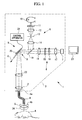
- an optical-scanning examination apparatus 1 includes an apparatus main body 3 provided with a first objective lens 2; an optical fiber bundle 4, one end 4a thereof being disposed at the image position of the first objective lens 2; and a second objective lens 5, which is disposed at another end 4b of the optical fiber bundle 4a and which images light emitted from the other end 4b onto a specimen A.
- a light source unit 6 that emits excitation light, an imaging unit 8 that includes an imaging device 7, such as a photomultiplier, that images return light returning from the specimen A, and an optical scanning unit 9 that two-dimensionally scans the excitation light emitted from the light source unit 6 are provided in the apparatus main body 3.
- the light source unit 6 includes a white-light source 10 such as a xenon lamp, an excitation filter 11 that transmits white light emitted from the white-light source 10 to produce excitation light of an excitation wavelength, a focusing lens 12 that focuses the excitation light radiated from the excitation filter 11, and a field stop 13 that limits the illumination region.
- the light source unit 6 also includes a focusing lens 14 that focuses the excitation light passing through the field stop 13 to form a first intermediate image.
- the imaging unit 8 includes a barrier filter 15 that transmits return light, such as reflection light or fluorescence, returning from the specimen A and that blocks the excitation light; a photometric filter 16 for measuring the intensity of the return light; and a focusing lens 17 that images the return light onto the imaging device 7.
- the imaging unit 8 also includes a focusing lens 18 that converges the return light coming from the first intermediate image position B to convert it to a collimated beam.
- the incident optical axis of the excitation light from the light source unit 6 and the optical axis of the imaging device 7 are disposed so as to intersect each other.
- a dichroic mirror 19 that selectively reflects the excitation light and transmits the other return light is placed at the intersection thereof.
- the optical scanning unit 9 is formed of a scanning mirror device 20, such as a digital micromirror device (DMD), which is formed of a plurality of minute mirrors 20a arrayed two-dimensionally.
- a scanning mirror device 20 such as a digital micromirror device (DMD)
- DMD digital micromirror device
- Each mirror 20a constituting the scanning mirror device 20 is selectively turned on and off in response to driving commands issued by an external control apparatus 21.
- excitation light incident from the light source 6 is reflected along the optical path directed towards the first objective lens 2, and the return light incident from the direction of the first objective lens 2 is reflected onto the optical path towards the imaging device 7.
- the excitation light and the return light are reflected in a direction away from these optical paths (in the direction of arrow C in Fig. 1 ).
- the scanning mirror device 20 constituting the optical scanning unit 9 is disposed at the first intermediate image position B formed by the focusing lens 14.
- a first intermediate image of the white-light source 10 is incident simultaneously on the plurality of mirrors 20a and is reflected towards the first objective lens 2 by the mirrors 20a in the on state.
- each mirror 20a can be switched on and off with an arbitrary driving pattern under the control of the control apparatus 21, as mentioned above.
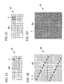
- Fig. 2A shows a driving pattern of a given format, where a single mirror 20a, indicated by oblique shading X, is in the on state.
- Fig. 2B shows an example driving pattern in which, within the mirrors 20a arranged in a square matrix, one mirrors 20a indicated by oblique shading X in all rows is sequentially turned on one at a time.
- the turned-on mirrors 20a in adjacent rows are disposed so as to be shifted in the row direction, and the turned-on mirrors 20a are switched in sequence in all rows, as indicated by the arrows in the figure, which allows two-dimensional scanning to be performed.
- Fig. 2C shows an example driving pattern in which a plurality of adjacent mirrors 20a are simultaneously turned on.
- Each mirror constituting the scanning mirror device 20 and a fiber core 25 of each optical fiber constituting the optical fiber bundle 4 are arranged in one-to-one correspondence, as shown in Fig. 3 .
- the excitation light reflected by that mirror 20a is made incident on a single predetermined fiber core 25.
- the light emitted from a single fiber core 25 is incident on a single mirror 20a that is associated in advance with that fiber core 25, to be reflected therefrom.
- Reference numeral 22 in the drawings represents an imaging lens positioned between the optical scanning unit 9 and the first objective lens 2. This imaging lens 22 converts the excitation light reflected at the optical scanning unit 9 into collimated light and introduces it to the first objective lens 2.
- Reference numeral 23 represents a monitor for displaying images captured by the imaging device 7.
- an operator freely moves a measuring head 24, provided with the second objective lens 5, with respect to the specimen A, to position the measuring head 24 at a suitable position for carrying out proper examination. Since the measuring head 24 is separated from the apparatus main body 3, which is relatively large, and is connected thereto by the optical fiber bundle 4, it can be placed at an appropriate position and orientation with respect to the specimen A by freely bending the optical fiber 4 as desired.
- each mirror 20a of the scanning mirror device 20 and each fiber core 25 of the optical fiber bundle 4 are arranged in one-to-one correspondence, the excitation light is transmitted by all of the fiber cores 25 and is imaged onto the specimen A by the second objective lens 5. Fluorescence produced at the specimen A passes back through the second objective lens 5, the optical fiber bundle 4, the first objective lens 2, the imaging lens 22, the scanning mirror device 20, the dichroic mirror 19, the focusing lens 18, the barrier filter 15, the photometric filter 16, and the focusing lens 17, and is captured by the imaging device 7.
- the operator switches to a measuring mode in which the scanning mirror device 20 is driven with a predetermined driving pattern under the control of the control apparatus 21.
- the excitation light emitted from the light source unit 6 is incident on the scanning mirror device 20 via the dichroic mirror 19, the excitation light is reflected at only the single mirror 20a that is turned on, and is made incident on the end of the corresponding fiber core 25 disposed at the end 4a of the optical fiber bundle 4 via the focusing lens 22 and the first objective lens 2.
- the excitation light transmitted in the optical fiber bundle 4 is then irradiated onto the specimen A via the second objective lens 5 and generates fluorescence in the specimen A.
- the fluorescence produced in the specimen A returns to the scanning mirror device 20 via the second objective lens 5, the optical fiber bundle 4, the first objective lens 2, and the focusing lens 22. Fluorescence is produced at many locations in the specimen A and is incident on the second objective lens 5. However, since the fiber cores 25 at the end 4a of the optical fiber bundle 4 and each mirror 20a in the scanning mirror element 20 are located at conjugate positions where the intermediate images are formed, only the fluorescence emitted from a location at a predetermined depth in the specimen A is imaged by the imaging unit 7 due to the confocal pinhole effect. Therefore, in the same way as using a normal fixed confocal pinhole, it is possible to acquire detailed fluorescence images of the interior of the specimen over a wide area at a predetermined depth.
- the excitation light reflected at the mirrors 20a of the scanning mirror device 20 can be made incident on the fiber cores 25 without impinging on cladding portions 26 of the optical fiber bundle 4. Therefore, an advantage is afforded in that the excitation light can be used efficiently without waste.
- the fluorescence emitted in the vicinity of the examination site away from the focal position located inside the specimen A can also pass through the end 4a of the optical fiber bundle 4 and the scanning mirror element 20. Therefore, although the confocal effect is reduced, on the other hand, the fluorescence intensity obtained at the imaging unit 7 is increased, which allows bright images to be acquired. In other words, this configuration is effective in applications where it is desired to carry out examination by means of bright fluorescence images, even though the resolution is somewhat low, and in applications where it is desired to acquire fluorescence images over a wide region in the depth direction.
- the optical scanning examination apparatus by controlling the on/off state of each mirror 20a constituting the scanning mirror device 20 in an arbitrary driving pattern using command signals from the control apparatus 21, it is possible to freely adjust the resolution of the obtained fluorescence images. At this time, when making the resolution lower, the fluorescence intensity is increased, which allows brighter images to be acquired, and it is therefore possible to carry out examination over a wide region in the depth direction.
- each mirror 20a in the scanning mirror device 20 and each fiber core 25 in the optical fiber bundle 4 are placed in one-to-one correspondence; however, instead of this arrangement, a one-to-many or a many-to-one correspondence may also be used.
- a one-to-many correspondence for example, 1-to-4, 1-to-9, etc.
- a many-to-one correspondence for example, 4-to-1, 9-to-1, etc.
- the resolution is reduced compared to the case of 1-to-1 correspondence; however, the intensity of the fluorescence obtained is increased, which allows bright fluorescence images to be acquired.
- the ratio of the fiber cores 25 and the associated mirrors 20a with respect to the total number of mirrors 20a constant, it is possible to acquire uniform fluorescence images that do not exhibit light and dark areas.
- a device in which the white-light source 10, such as a xenon lamp or mercury lamp, and the excitation filter 11 are combined may be used as the light source unit 6; instead of this, however, a laser light source may be employed.
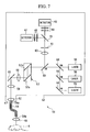
- the optical-scanning examination apparatus 30 differs from the optical-scanning examination apparatus according to the first example in that a light source unit 31, including a laser light source 32 and a cylindrical lens 33, produces a band of collimated light, and the structure of an optical scanning unit 34 is different.
- the light source unit 31 includes a collimator lens 35, which converts the laser light emitted by the laser light source 32 into a collimated beam.
- the optical scanning unit 34 includes a scanning mirror device 37 that reflects the band of laser light emitted by the light source unit 31 at a first intermediate image position B of a focusing lens 36; a collimator lens 38 that converts the laser light reflected at the scanning mirror device 37 into a band of collimated light; a galvano mirror 39 that reflects the band of collimated light emitted from the collimator lens 38; and a pupil projection lens 40 that focuses the laser light reflected by the galvano mirror 39 to form a third intermediate image at a third intermediate image position D.
- the scanning mirror device 37 includes a plurality of mirrors 37a disposed in a row at the position where the band of laser light L is incident simultaneously. By sequentially changing the on/off state of each mirror 37a in the arrayed direction, the laser light L can be scanned in one direction.
- the galvano mirror 39 is rotated by a motor 41 about an axis positioned within the horizontal plane in which the laser light L is scanned by the scanning mirror device 37. With this configuration, the laser light L scanned in one direction by the scanning mirror device 37 can be scanned in a direction perpendicular thereto by the galvano mirror 39.
- the laser light is scanned in two dimensions by the optical scanning unit 34 to be made incident on the end 4a of the optical fiber bundle 4.
- the optical-scanning examination apparatus having such a configuration, by combining the scanning mirror device 37, which is formed of a single row of arrayed mirrors, and the single-axis galvano mirror 39, it is possible to scan the specimen A in two dimensions with a simple configuration.
- the scanning mirror device 37 which is formed of a single row of arrayed mirrors
- the single-axis galvano mirror 39 it is possible to scan the specimen A in two dimensions with a simple configuration.
- the intensity of the laser light L reflected by the individual mirrors 37a making up the scanning mirror device 37 can be increased. Therefore, high-intensity laser light L can be made incident on the specimen A, which allows bright fluorescence images to be obtained.
- a device having a single row of arrayed mirrors 37a is used as the scanning mirror device 37; however, instead of this, a device having two or more rows of mirrors may be employed, as shown in Fig. 6 (for example, four rows are shown in Fig. 6 ).
- a device having two or more rows of mirrors may be employed, as shown in Fig. 6 (for example, four rows are shown in Fig. 6 ).
- an optical-scanning confocal examination apparatus 51 which is a laser-scanning confocal microscope, includes an apparatus main body 53 having a first objective lens 52; an optical fiber bundle 54 of which one end 54a is disposed at an image position of the first objective lens 52; and a second objective lens 55, which is disposed at the other end 54b of the optical fiber bundle 54 and which images the light emitted from the other end 54b onto a specimen A.
- the apparatus main body 53 contains laser light sources 56 that generate laser light; an optical scanning unit 57, formed of two galvano mirrors 57a and 57b that can be oscillated around two orthogonal axes, that two-dimensionally scans the laser light emitted from the laser light sources 56 onto the end 54a of each optical fiber constituting the optical fiber bundle 54; a pupil projection lens 58; an imaging lens 59; a dichroic mirror 60 that splits off returning laser light that returns via the first objective lens 52; a confocal pinhole 61 disposed at the conjugate position of the end 54a of the optical fiber bundle 54; and an optical detector 62 that detects light passing through the confocal pinhole 61.
- Reference numeral 63 in the figure represents a confocal lens.
- a plurality of laser light sources 56 is provided, to allow the specimen A to be irradiated with laser light of different wavelengths; however, a single laser light source 56 may be used.
- a plurality of optical detectors 62 is shown as an example, but a single optical detector 62 may be used.
- Reference numerals 64 and 70 represent dichroic mirrors, and reference numeral 65 represents a bandpass filter. Also, reference numeral 66 represents a light-path folding mirror.
- the light emitted from the other end 54b of the optical fiber bundle 54 serves as a light source for the second objective lens 55 and is imaged at a desired location on the specimen A.
- a glass plate 67 is fixed to the end 54a of the optical fiber bundle 54.
- This glass plate 67 has a desired thickness, for example, a thickness of about 2 mm.
- the glass plate 67 is placed in contact with the end 54a of the optical fiber bundle 54 so as to abut the end 54a (physical contact).
- An adhesive with substantially the same refractive index as the glass plate 67 and the core of each fiber making up the optical fiber bundle 54 is preferably provided between the glass plate 67 and the end 54a of the optical fiber bundle 54, ideally without an air gap.
- the laser light passes through the dichroic mirrors 64 and 60 and is made incident on the optical scanning unit 57 to be scanned in two dimensions.
- the irradiated laser light deflected by the optical scanning unit 57 is made incident on the end 54a of the optical fiber bundle 54 via the pupil projection lens 58, the mirror 66, the focusing lens 59, and the first objective lens 52.
- the laser light incident on the end 54a of the optical fiber bundle 54 and transmitted through the optical fiber bundle 54 diverges from the other end 54b of the optical fiber bundle 54 and is irradiated onto an examination site of the specimen A by the second objective lens 55 disposed at the subsequent stage. Fluorescence is emitted from the examination site of the specimen A irradiated with this laser light, and the fluorescence returns via the second objective lens 55, the optical fiber bundle 54, the first objective lens 52, the focusing lens 59, the mirror 66, the pupil projection lens 58, and the optical scanning unit 57, is reflected by the dichroic mirror 60, and is split off from the laser light.
- the optical detector 62 Since the end 54a of the optical fiber bundle 54 functions as a confocal pinhole and is disposed at a conjugate position of the confocal pinhole 61, only the light emitted from the end 54a of the optical fiber bundle 54 is allowed to pass through the confocal pinhole 61 to be detected by the optical detector 62.
- the light made incident on the end 54a of the optical fiber bundle 54 by the first objective lens 52 is incident from the surface of the glass plate 67 before being introduced to the end 54a. Therefore, since the glass plate 67 and the cores of the optical fiber bundle 54 are bonded without an air gap therebetween, the light passes through the interface between media having the same refractive indexes. In this case, there is substantially no reflection of the laser light at the interface. Only slight reflection of the laser light occurs, but since the reflected laser light is scattered by the glass plate 67, as shown by the arrow in Fig. 8 , the reflected light returning to the first objective lens 52 is extremely small.
- the laser light When the laser light is incident on the surface of the glass plate 67 from the air, it is transmitted through the interface between media having different refractive indices, and therefore, part of the light is reflected at the surface of the glass plate 67.
- the glass plate since the glass plate has a certain thickness, that part of the light is kept away, in the optical axis direction, from the end 54a of the optical fiber bundle 54 functioning as a confocal pinhole. Therefore, even though it returns towards the optical detector 62, it is not possible for most of the reflected light produced at the surface of the glass plate 67 to be transmitted through confocal pinhole 61 disposed at the stage before the optical detector 62, thus preventing it from being detected by the optical detector 62.
- the occurrence of flare can be prevented, which allows detailed fluorescence images to be acquired and improves the examination accuracy.
- the glass plate 67 is disposed at the end 54a of the optical fiber bundle 54 so as to be directly bonded thereto; instead of this, however, as shown in Fig. 9 , they may be connected together by means of a transparent adhesive 68. With this configuration, it is possible to more reliably prevent the formation of an air gap between the glass plate 67 and the end 54a of the optical fiber bundle 54, which allows the occurrence of reflected light at the end 54a of the optical bundle 54 to be suppressed.
- a barrier filter 69 for cutting reflected laser light may be disposed in the region from the end 54a of the optical fiber bundle 54 to the optical detector 62.
- the optical scanning unit 57 formed of the galvano mirrors 57a and 57b is provided; instead of this, however, as shown in Fig. 11 , a confocal scanner 75 in which a focusing disk 71 and a pinhole disk 72 are connected by a drum 73 and rotatably driven by a motor 74 may be used.
- the focusing disk 71 includes a plurality of Fresnel lenses formed on one side of a substrate, and the Fresnel lenses are arranged so as to be sequentially staggered in the radial direction by a certain distance.
- the pinhole disk 72 has a plurality of pinholes in a substrate, and the pinholes are arranged so as to be sequentially staggered in the radial direction by a certain distance.
- a beamsplitter 76 is disposed between the focusing disk 71 and the pinhole disk 72, and returning fluorescence passing through pinholes in the pinhole disk 72 is split off by the beamsplitter 76 and is imaged by a camera 78, via the barrier filter 69 and the focusing lens 77.
- the laser light emitted from the laser light source 56 passes through a plurality of pinholes simultaneously, thus allowing the specimen A to be scanned with multiple spots of laser light. It is therefore possible to acquire fluorescence images of the specimen A at high speed. In this case, since the reflected light is blocked at the end 54a of the optical fiber bundle 54, it is possible to sufficiently reduce the level of flare occurring in the fluorescence images captured by the camera 78. Additional Items
- the invention may also provide an optical-scanning confocal examination apparatus including an apparatus main body that scans light from a light source and focuses the light with a first objective lens; an optical fiber bundle of which one end is disposed at the focal position of the first objective lens; a second objective lens, disposed at the other end of the optical fiber bundle, for focusing the light emitted from the other end of the optical fiber bundle onto a specimen; a confocal pinhole, disposed at the conjugate position of the one end of the optical fiber bundle, that allows return light returning from the specimen via the second objective lens, the optical fiber bundle, and the first objective lens to pass therethrough; and an imaging unit that images the light passing through the confocal pinhole.
- a glass plate of predetermined thickness is disposed on the one end of the optical fiber bundle.
- the position and angle of the second objective lens can be freely set by bending the optical fiber bundle. Also, by disposing the second objective lens at the end of the optical fiber bundle, the end portion can be reduced in size and can thus be easily positioned at a narrow examination site or in a small specimen, such as a small experimental animal.
- the light emitted from the light source and focused at the end of the optical fiber bundle by the first objective lens is incident on the end of the optical fiber bundle after becoming incident on the glass plate disposed at the end of the optical fiber bundle.
- the light incident on the optical fiber bundle is then transmitted through the optical fiber bundle and is focused on the specimen by the second objective lens.
- Light emitted from the specimen then returns via the second objective lens, the optical fiber bundle, and the first objective lens, and passes through the confocal pinhole to be imaged by the imaging unit. Since the end of the optical fiber and the confocal pinhole are placed at conjugate positions, only the light transmitted through the end of the optical fiber bundle is imaged by the imaging unit.
- the light propagating towards the end of the optical fiber bundle from the first objective lens is partially reflected when entering the glass plate; however, since the glass plate has a certain thickness, most of the light reflected at the surface of the glass plate cannot pass through the confocal pinhole. Also, if the glass plate and the end of the optical fiber bundle are bonded together, the light incident on the optical fiber bundle from the glass plate is transmitted since these media have the same refractive indices, and therefore, substantially no reflected light is produced.
- the reflected light is scattered when being emitted back into the air from the surface of the glass plate, and therefore, almost none of it passes through the confocal pinhole, in the same way as described above.
- the reflected light imaged by the imaging means is reduced, which allows low-noise images to be acquired.
- the glass plate may be bonded to the end of the optical fiber bundle.
- the present invention may also provide an optical-scanning confocal examination apparatus including an apparatus main body that scans light from a light source and focuses the light with a first objective lens; an optical fiber bundle of which one end is disposed at the focal position of the first objective lens; a second objective lens, disposed at the other end of the optical fiber bundle, that focuses the light emitted from the other end of the optical fiber bundle onto a specimen; a confocal pinhole which is disposed at a conjugate position of the one end of the optical fiber bundle and which allows return light returning from the specimen via the second objective lens, the optical fiber bundle, and the first objective lens to pass therethrough; and an imaging unit that images the light passing through the confocal pinhole.
- a barrier filter that blocks reflected light from the end of the optical fiber bundle is provided between the one end of the optical fiber bundle and the imaging unit.
- the barrier filter since reflected light from the end of the optical fiber bundle is blocked by the action of the barrier filter, it is possible to acquire images having low noise, such as flare caused by reflected light, in the same way as described above.
- the barrier filter may be an optical element having barrier characteristics placed in the light path from the end of the optical fiber bundle to the imaging unit.
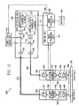
- Fig. 12 shows a schematic diagram of an examination apparatus according to a fourth example of the present invention.
- an examination apparatus 100 of this embodiment includes a stage 170 for carrying a specimen 180 (for example, an experimental animal such as a mouse); a laser light source unit 110 that generates a plurality of laser beams; a plurality of optical irradiation/detection units 140 that irradiate the plurality of light beams onto the specimen 180 and detect light from the specimen 180; an image-detecting unit 120 that photoelectrically converts the light beams emitted from the plurality of light irradiation/detection unit 140 to generate an image signal; a plurality of optical fibers 130 that optically connect the image-detecting unit 120 and the plurality of light irradiation/detection units 140; a control unit 150 for controlling the overall apparatus; and a monitor 160 for displaying examination information such as images.
- a specimen 180 for example, an experimental animal such as a mouse
- a laser light source unit 110 that generates a plurality of laser beams
- the laser light source unit 110 if formed, for example, of a plurality of lasers and optical elements and can emit laser beams of a plurality of wavelengths.
- the laser light source unit 110 may be formed of one laser and an optical element that splits the output laser light into a plurality of light beams so as to emit laser beams having the same wavelength.
- the light irradiation/detection units 140 each include a collimator lens 141, XY galvano mirrors 142, a pupil lens 143, an imaging lens 144, and an objective lens 145.
- the pupil lens 143, the imaging lens 144, and the objective lens 145 constitute an optical system 146 for irradiating a converging laser beam onto the specimen 180 and for detecting detection light produced by the specimen 180 in response to the irradiated laser light.
- the collimator lens 141 is for optically coupling with the optical fiber 130; the collimator lens 141 guides the laser light from the optical fiber 130 to the optical system 146 via the XY galvano mirrors 142 and also converges the light beam detected by the optical system 146 to introduce it back into the optical fiber 130.
- the XY galvano mirrors 142 include a mirror that can oscillate about the X-axis and a mirror that can oscillate about the Y-axis, which allows the incident light beam to be two-dimensionally scanned in the X-axis and Y-axis directions.
- the XY galvano mirrors 142 constitute a scanning unit for scanning the region that generates detection light, which is photoelectrically converted by the image-detection unit 120.
- the detection unit is not limited to XY galvano mirrors; another scanning mechanism that scans a light beam may also be used.
- the image-detection unit 120 includes excitation dichroic mirrors 121, collimator lenses 122, confocal pinholes 125, filters 126, and photoelectric conversion elements 127.
- the excitation dichroic mirrors 121 selectively reflect only light of specific wavelengths from the laser light emitted by the laser light source unit 110 and transmit light of other wavelengths.
- the collimator lenses 122 are for optically coupling to the optical fibers 130; the collimator lenses 122 converge the laser beams from the excitation dichroic mirrors 121 to introduce the laser beams into the optical fibers 130 and also guide light from the optical fibers 130 to the excitation dichroic mirrors 121.
- the confocal pinholes 125 are placed in confocal positional relationship with the spots (regions that generate detection light) of the laser beams irradiating the specimen 180, so as to selectively allow only light from the vicinity of the spots (regions that generate detection light) to pass therethrough and to block light from other parts.
- the confocal pinholes 125 are provided for acquiring confocal images, but they may be omitted if it is not necessary to acquire confocal images.
- the filters 126 selectively transmit only light of the wavelengths desired to be detected, and block light of unwanted wavelengths.
- the photoelectric conversion elements 127 are formed, for example, of PMTs (photomultipliers) or PDs (photodiodes); they function as photoelectric conversion devices for photoelectrically converting the detection light and photoelectrically convert the light transmitted through the filters 126 to generate an image signal of one pixel.
- Each of the excitation dichroic mirrors 121 and each of the filters 126 can be changed among a plurality of excitation dichroic mirrors and a plurality of filters, respectively, using electric motors, and one of a plurality is selectively placed in the optical path.
- Fig. 12 shows only one placed in the optical path, however.
- the control unit 150 includes an image processing unit 152 for processing the image signal produced in the image-detecting unit 120 to form an image and an image recording unit 154 that records the image formed in the image processing unit 152.
- the control unit 150 is also provided with a function for controlling the XY galvano mirrors 142 constituting the scanning unit.
- the control unit 150 is formed, for example, of a computer and a dedicated expansion board.
- the monitor 160 is formed, for example, of a CRT and functions as an image display apparatus for displaying images formed in the image processing unit.
- two light irradiation/detection units 140 are shown in Fig. 12 ; however, the examination apparatus 100 may include two or more light irradiation/detection units 140.
- two optical systems (the excitation dichroic mirrors 121, the collimator lenses 122, the confocal pinholes 125, the filters 126, and the photoelectric conversion elements) for photoelectrically converting the light detected in the light irradiation/detection units 140 are depicted in the image-detecting unit 120; however, the image-detecting unit 120 may be provided with the same number of optical systems as the number of light irradiation/detection units 140, or more. In other words, the image-detecting unit 120 can be connected to a plurality of light irradiation/detection units 140.
- the image-detecting unit 120 in Fig. 12 is configured to detect only light of one wavelength per laser beam; however, it may be configured to detect light of a plurality of wavelengths per laser beam.
- the image-detecting unit 120 selectively reflects light of specific wavelengths, but it may include a beamsplitter that transmits light of other wavelengths in the optical path between the confocal pinhole 125 and the filter 126, and it may include an additional filter 126 and photoelectric conversion element 127 in the light path split off by the beamsplitter.
- the laser light source unit 110 emits laser beams of a specified wavelength or wavelengths and with a specified intensity, according to settings from the control unit 150.
- the laser beams emitted from the laser light source unit 110 are introduced to the image-detecting unit 120.
- the laser beams introduced to the image-detecting unit 120 are reflected by the excitation dichroic mirrors 121, are converted to converging laser beams by the collimator lenses 122, and are introduced to the optical fibers 130.
- the laser beams introduced into the optical fibers 130 are transmitted through the optical fibers 130, and are emitted from the optical fibers 130 to be incident on the light irradiation/detection units 140.
- the laser beams entering the light irradiation/detection units 140 are converted to collimated beams by the collimator lenses 141 and are incident on the XY galvano mirrors 142.
- the laser beams reflected by the XY galvano mirrors 142 are converted to converging beams by the optical systems 146 formed of the pupil lenses 143, the imaging lenses 144, and the objective lenses 145, and are irradiated onto the specimen 180.
- the laser beams irradiated onto the specimen 180 form spots at the focal planes (examination planes) of the optical systems 146.
- the XY galvano mirrors 142 scan the laser beams horizontally and vertically so that the laser beam spots are scanned over the examination planes (focal planes of the optical systems 146) in the specimen 180.
- the specimen 180 receiving the laser light is a fluorescent specimen, it generates fluorescence as the detection light, and if it is a reflective specimen, it produces reflected light as the detection light.
- the fluorescence is then guided to the image-detecting unit 120 via the objective lenses 145, the imaging lenses 144, the pupil lenses 143, the XY galvano mirrors 142, the collimator lenses 141, and the optical fibers 130.
- the detection light beams introduced into the image-detecting unit 120 are converted to collimated beams by the collimator lenses 122 and are incident on the excitation dichroic mirrors 121. Since the excitation dichroic mirrors 121 have a characteristic whereby they transmit the detection light wavelengths, the detection light passes through the excitation dichroic mirrors 121.
- the excitation dichroic mirrors 121 In the detection light passing through the excitation dichroic mirrors 121, only light from the vicinity of the spots on the examination plane passes through the confocal pinholes 125. Light of unwanted wavelengths is removed from the detection light passing through the confocal pinholes 125 by the filters 126, and the remaining light is incident on the photoelectric conversion elements 127. The detection light incident on the photoelectric conversion elements 127 is photoelectrically converted to output image signals to the control unit 150.
- the image-processing unit 152 in the control unit 150 subjects the luminance data of the detection light output from the image-detecting unit 120 as the image signals to analog-to-digital conversion, and arranges the luminance data based on horizontal synchronization and vertical synchronization. By outputting the arranged luminance data to the monitor 160 to display an image, an image of the examination location on the specimen 180 can be formed. Also, since the control unit 150 can synchronize signals from the plurality of photoelectric conversion elements 127 to process them, it is possible to form simultaneous images of multiple positions on the specimen (for example, position A and position B). In other words, separate positions on the specimen A can be simultaneously examined.
- Fig. 12 shows an example in which separate positions on the specimen are simultaneously examined with the plurality of light irradiation/detection units 140; however, it is of course possible to simultaneously examine the same position on the specimen with the plurality of light irradiation/detection units 140.
- All of the plurality of light irradiation/detection units 140 need not be used for the same type of examination; they may be used for different types of examination.
- the plurality of light irradiation/detection units 140 may include multiple types of light irradiation/detection units 140.
- the plurality of light irradiation/detection units 140 may include light irradiation/detection units designed for fluorescence examination and light irradiation/detection units designed for reflection examination. With this configuration, it is possible to carry out fluorescence examination and reflection examination simultaneously. In this case, for example, reflection examination can be carried out in the image-detecting unit 120 by detecting the same wavelength as that of the laser light, and fluorescence examination can be carried out by detecting different wavelengths from that of the laser light.
- all of the plurality of light irradiation/detection units 140 need not be used for examination; they may be used for color fading applications in which the specimen 180 is made to fade depending in the intensity of the light, or for optical stimulus applications in which a capsule inserted into a specimen to be stimulated is broken down by light and a stimulus is applied to the specimen.
- an optical stimulus is applied by the light irradiation/detection unit 140 to the position A on the specimen, and the change due to the optical stimulus can be examined with a separate light irradiation/detection unit 140 disposed at another position B on the specimen.
- the number of light irradiation/detection units 140 used for optical stimulation is not restricted, it is possible to conduct various types of experiment.
- a region outside the field of view of one of the light irradiation/detection units 140 can be examined with another light irradiation/detection unit 140, which allows multiple positions on a large specimen to be examined simultaneously.
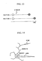
- Fig. 14 shows a typical nerve. As shown in Fig. 14 , it is widely known that nerves are widely disposed throughout the bodies of animals for transmitting electrical signals. In a nerve structure, a dendrite splits off from an axon, which is the main part and includes a nucleus, and there is a part called a spine in the vicinity of the dendrite.
- transmission at a multiple positions of nerve cells the relationships between soma and neurons of nerve cells, dendrites and soma, multiple dendrites at other positions, multiple spines at other positions, and so on can be examined.
- organs for example, blood vessels
- organs for example, blood vessels
- FIG. 15 schematically shows an examination apparatus according to a fifth embodiment of the present invention.
- Elements in Fig. 15 having the same reference numerals as those in Fig. 12 represent the same parts, and a description thereof is omitted.
- an examination apparatus 200 of this embodiment includes light irradiation/detection units 240 instead of the light irradiation/detection units 140 in the fourth embodiment, an image-detecting unit 220 in place of the image-detecting unit 120 of the fourth embodiment, and optical fiber bundles 230 in place of the optical fibers 130 in the fourth example.
- the light irradiation/detection units 240 each include a collimator lens 141, a pupil lens 143, an imaging lens 144, and an objective lens 145.
- the light irradiation/detection units 240 have a configuration in which the XY galvano mirrors 142 in the light irradiation/detection units 140 of the fourth example are omitted.
- the light irradiation/detection units 240 of this example can have a more compact configuration compared to the light irradiation/detection units 140 of the fourth example.
- the image-detecting unit 220 includes excitation dichroic mirrors 121, collimator lenses 122, XY galvano mirrors 142, confocal pinholes 125, filters 126, and photoelectric conversion elements 127.
- the XY galvano mirrors 142 are positioned in the optical path between the excitation dichroic mirrors 121 and the collimator lenses 122.
- the XY galvano mirrors include a mirror that can oscillate about the X-axis and a mirror that can oscillate about the Y-axis, which allows the incident light beam to be scanned two-dimensionally in the X-axis and Y-axis directions.
- the remaining structure is the same as the image-detecting unit 120 of the fourth example.
- the optical fiber bundles 230 can transmit the scanned light beams.
- the optical fiber bundles 230 can transmit the incident light and can emit it from a position corresponding to the incident position.
- the laser light source unit 110 emits laser beams of a specified wavelength or wavelengths and with a specified intensity, according to settings from the control unit 150.
- the laser beams emitted from the laser light source unit 110 are introduced to the image-detecting unit 220.
- the laser beams introduced to the image-detecting unit 220 are reflected by the excitation dichroic mirrors 121, pass the XY galvano mirrors 142, are converged by the collimator lenses 122, are introduced to the optical fiber bundles 230, and are transmitted through the optical fiber bundles 230 to be incident on the light irradiation/detection units 240.
- the incident laser beams are converted to collimated beams by the collimator lenses 141, are converted to converging beams by the optical systems 146 formed of the pupil lenses 143, the imaging lenses 144, and the objective lenses 145, and are irradiated onto the specimen 180.
- the laser beams irradiated onto the specimen 180 form spots at the focal planes of the optical systems 146.
- the laser beams converged by the collimator lenses 122 are smaller in diameter than the ends of the optical fiber bundles 230 and thus illuminate only a small region of the ends of the optical fiber bundles 230.
- the galvano mirrors 142 scan the laser beams in the horizontal direction and the vertical direction. Accordingly, the laser beams converged by the collimator lenses 122 are scanned on the ends of the optical fiber bundles 230.
- the laser beams incident on the optical fiber bundles 230 are transmitted through the optical fiber bundles 230 and are emitted from positions on the ends of the optical fiber bundles 230 corresponding to the incident positions.
- the exit positions of the laser beams emitted into the light irradiation/detection units 240 are scanned on the ends of the optical fiber bundles 230 in response to the scanning of the laser beams by the XY galvano mirrors 142.
- the laser beam spots formed at the examination planes in the specimen 180 are scanned.
- the specimen 180 receiving the laser light is a fluorescent specimen, fluorescence is generated as detection light, and if the specimen 180 is a reflective specimen, reflection light is produced as the detection light.
- the detection light is guided to the image-detecting units 220 via the objective lenses 145, the imaging lenses 144, the pupil lenses 143, the collimator lenses 141, and the optical fiber bundles 230.
- the detection light beams entering the image-detecting unit 220 are converted to collimated beams by the collimator lenses 122, pass the XY galvano mirrors 142, and are incident on the excitation dichroic mirrors 121. Since the excitation dichroic mirrors 121 have characteristics whereby they transmit the wavelengths of the detection light, the detection light passes through the excitation dichroic mirrors 121.
- the control unit 150 In the detection light passing through the excitation dichroic mirrors 121, only the light from the vicinity of the spots on the examination planes passes through the confocal pinholes 125. Light of unwanted wavelengths is removed from the detection light passing through the confocal pinholes 125 by the filters 126, and the remaining light is incident on the photoelectric conversion elements 127. The detection light incident on the photoelectric conversion elements 127 is photoelectrically converted and output as image signals to the control unit 150.
- the image processing unit 152 in the control unit 150 subjects the detection light luminance data output from the image-detecting unit 220 as image signals to analog-to-digital conversion, and arranges the luminance data based on horizontal synchronization and vertical synchronization. By outputting the arranged luminance data to the monitor 160 to display it thereon, it is possible to form images of the examination positions of the specimen 180. Also, since the control unit 150 can synchronize a plurality of signals from the photoelectric conversion elements 127 to process them, it is possible to simultaneously form images of a plurality of positions on the specimen 180 (for example, position A and position B).
- this examination apparatus 200 similarly to the fourth example, it is possible to examine a region outside the field of view of the objective lens 145 in one light irradiation/detection unit 240 with another light irradiation/detection unit 240. Therefore, it is possible to simultaneously examine a plurality of positions on a large specimen.
- the main difference between this example and the fourth example is the position of the scanning unit.
- the scanning unit is provided in the image-detecting unit 220 and the number of components in the light irradiation/detection units 240 is small, it is possible to make the light irradiation/detection units 240 more compact.
- the area occupied in the vicinity of the specimen is lower than in the fourth example, the number of possible positions of the light irradiation/detection units 240 can be increased, which affords an advantage in that the degree of freedom in terms of position, angle, and so on can be improved.
- Fig. 16 schematically shows an examination apparatus according to a sixth example of the present invention.
- the examination apparatus of this example is similar to the examination apparatus of the fifth example shown in Fig. 15 .
- the parts indicated by the same reference numerals as the parts shown in Fig. 15 represent the same parts, and a detailed description thereof is thus omitted.
- an examination apparatus 300 of this example includes a lamp light source unit 310 instead of the laser light source unit 110 in the fifth example, and an image-detecting unit 320 instead of the image-detecting unit 220 in the fifth example.
- the lamp light source unit 310 includes a lamp light source for illumination, for example, a mercury lamp or the like.
- the lamp light source unit 310 emits a plurality of illumination light beams whose diameter is large compared to that of laser beams.
- the configuration of the light irradiation/detection units 240 is the same as those in the fifth example.
- the image-detecting unit 320 includes excitation filters 321, dichroic mirrors 332, collimator lenses 122, rotating-disk pinholes 325, filters 326, and area sensors 327.
- the excitation filters 321 transmit only light of specified wavelengths in the illumination light from the lamp light source unit 310.
- the dichroic mirrors 322 reflect only light of the excitation wavelengths and transmit light of other wavelengths.
- the rotating-disk pinholes 325 include a plurality of pinholes and can be rotated.
- the pinholes in the rotating-disk pinholes 325 selectively allow only detection light from the parts which are in confocal positional relationship therewith, in the focal plane of the optical systems 146 in the light irradiation/detection units 240, and block light coming from other parts.
- the rotating-disk pinholes 325 function as confocal pinholes.
- the pinholes in the rotating-disk pinholes 325 move with the rotation of the rotating-disk pinholes 325.
- the regions that generate detection light, which can pass through the pinholes in the rotating-disk pinholes 325 move. Therefore, the rotating-disk pinholes 325 also effectively function as scanning units that scan the regions generating detection light.
- the area sensors 327 are formed, for example, of a CCD or PMT array; they function as photoelectric devices for photoelectrically converting the detection light, and include multiple photoelectric conversion parts (pixels) arrayed, for example, in a matrix. This allows information from a plurality of photoelectric conversion parts (pixels) to be acquired simultaneously.
- the rotating-disk pinholes 325 are provided for acquiring confocal images; however, if it is not necessary to acquire confocal images, they may be omitted.
- Fig. 16 shows an example in which two light irradiation/detection units 240 are provided; however, the examination apparatus 300 may include two or more light irradiation/detection units 240.
- Two optical systems (the excitation filters 321, the dichroic mirrors 322, the collimator lenses 126, the rotating-disk pinholes 325, the filters 326, and the area sensors 327) for photoelectrically converting the light detected in the light irradiation/detection units 240 are depicted in the image-detecting unit 320, corresponding to the two light irradiation/detection units 230; however, the image-detecting unit 320 may include the same number of optical systems as the light irradiation/detection units 240 or greater.
- the image-detecting unit 320 in Fig. 16 has a configuration in which only light of one wavelength per illumination beam is detected; however, a configuration in which multiple wavelengths per illumination beam are detected may also be used. In this case, the image-detecting unit 320 selectively reflects light of a specified wavelength; however, a beamsplitter that transmits light of other wavelengths may be disposed in the optical path between the rotating-disk pinholes 325 and the filters 326, and another filter 326 and area filter 327 may be disposed in the optical path split off by the beamsplitter.
- the control unit 150 is formed of, for example, a computer and a dedicated expansion board, and has function for controlling the rotation of the rotating-disk pinholes 325 constituting the scanning unit.
- the lamp light source unit 310 emits illumination beams according to a brightness setting from the control unit 150.
- the illumination beams from the lamp light source unit 310 are introduced to the image-detecting unit 320. From the illumination beams introduced to the image-detecting unit 320, only light of specific wavelengths is selectively transmitted by the excitation filters 321.
- the illumination beams transmitted through the excitation filters 321 are reflected by the dichroic mirrors 322 and are converged by the collimator lenses 122 to be introduced to the optical fiber bundles 230.
- the illumination beams converged by the collimator lenses 122 illuminate substantially the entire end faces of the optical fiber bundles 230.
- the illumination beams introduced into the optical fiber bundles are then transmitted through the optical fiber bundles 230 to be introduced to the light irradiation/detection units 240.
- the illumination beams entering the light irradiation/detection units 240 are converged by the optical systems 146 formed of the pupil lenses 143, the imaging lenses 144, and the objective lenses 145 and are irradiated onto the specimen 180.
- the illumination beams irradiated onto the specimen 180 illuminate a relatively wide area at the focal planes (examination planes) of the optical systems 146.
- the specimen 180 receiving the illumination light is a fluorescent specimen, fluorescence is produced as detection light, and if the specimen 180 is a reflective specimen, reflection light is produced as the detection light.
- the detection light is then guided to the image-detecting unit 320 via the objective lenses 145, the imaging lenses 144, the pupil lenses 143, the collimator lenses 141, and the optical fiber bundles 230.
- the detection beams entering the image-detecting unit 320 are converted to collimated beams by the collimator lenses 122 and are incident on the dichroic mirrors 322. Since the dichroic mirrors 322 have characteristics whereby they transmit the detection light wavelengths, the detection light is transmitted through the dichroic mirrors 322.
- the rotating-disk pinholes 325 are disposed orthogonally to the optical axis and rotate. Therefore, their function is effectively the same as the regions that generate detection light being scanned over one frame of the area sensors 32.
- Light of unwanted wavelengths is removed from the detection light passing through the rotating-disk pinholes 325 by the filters 326, and the remaining light is incident on the area sensors 327.
- the detection light incident on the area sensors 327 is then photoelectrically converted and is output to the control unit 150 as an image signal of one frame.
- the detection light data output from the image-detecting unit 320 as image signals is sequentially output to the monitor 160 for each frame and is displayed. With the arrangement described above, it is possible to simultaneously form images of a plurality of positions (for example, position A and position B) on the specimen 180.
- the examination apparatus 300 of this example it is possible to examine a region outside the field of view of the objective lens 145 of one light irradiation/detection unit 240 with another light irradiation/detection unit 240, which enables simultaneous examination of a plurality of positions on a large specimen.
- the main difference between the present example and the fifth example is that an area sensor such as a CCD or PMT array is used in the photoelectric conversion device, which allows images to be acquired at high speed.
- an area sensor such as a CCD or PMT array is used in the photoelectric conversion device, which allows images to be acquired at high speed.
- Fig. 17 schematically shows an examination apparatus according to a seventh example.
- the examination apparatus of this example is similar to the examination apparatus of the fifth example shown in Fig. 15 and the examination apparatus of the sixth example shown in Fig. 16 .
- parts indicated with the same reference numerals as parts shown in Fig. 15 and Fig. 16 represent the same parts, and a detailed description thereof is thus omitted.
- an examination apparatus 400 of this example includes a light source unit 410 in place of the laser light source unit 110 of the fifth example and the lamp light source unit 310 of the sixth example, and also includes an image-detecting unit 420 in place of the image-detecting unit 220 of the fifth example and the image-detecting unit 320 of the sixth example.
- the examination apparatus 400 of this example includes two light irradiation/detection units 240A and 240B.
- the examination apparatus 400 may also include other light irradiation/detection units, however.
- the two light irradiation/detection units 240A and 240B have a similar configuration to the light irradiation/detection units 240 of the fifth embodiment; however, the two light irradiation/detection units 240A and 240B include objective lenses 145A and 145B, respectively, having different magnifications.
- the two light irradiation/detection units 240A and 240B are respectively positioned above and below the specimen 180. Instead of being provided with objective lenses having different magnifications, the two light irradiation/detection units 240A and 240B may be provided with objective lenses having different fields of view.
- the light source unit 410 includes a lamp light source that produces an illumination beam that is irradiated from the light irradiation/detection unit 240A and a laser that produces a laser light beam that is irradiated from the light irradiation/detection unit 240B.
- the image-detecting unit 420 includes two optical systems having a function of photoelectrically converting detection light and scanning function, corresponding to the two light irradiation/detection units 240A and 240B.
- the optical system for the light irradiation/detection unit 240A is formed of an excitation filter 321, a dichroic mirror 322, a collimator lens 122, a rotating-disk pinhole 325, a filter 326, and an area sensor 327, similar to the sixth example.
- the optical system for the light irradiation/detection unit 240B is formed of a dichroic mirror 121, XY galvano mirrors 142, a collimator lens 122, a confocal pinhole 125, a filter 126, and a photoelectric conversion element 127, similar to the fifth embodiment.
- the XY galvano mirrors 142 constitute one scanning unit, and the rotating-disk pinhole 325 constitutes another scanning unit. In other words, the two scanning units have different structures.
- the control unit 150 allows both synchronized operation and independent operation of the two scanning units formed of the XY galvano mirrors 142 and the rotating-disk pinhole 325.
- the description "synchronized operation of the two scanning units" used here means operation wherein the two scanning units are associated in some way. For example, this includes the case where a wide region is scanned at low speed with one of the scanning units while a narrow region contained in the wide region is scanned at high speed with the other scanning unit.
- the light source unit 410 emits an illumination beam according to an intensity setting from the control unit 150. Also, the light source unit 410 emits laser a laser beam of a specific wavelength and a specific intensity according to settings from the control unit 150.
- the illumination beam entering the image-detecting unit 420 from the light source unit 410 is for the light irradiation/detection unit 240A, and the laser beam entering the image-detecting unit 420 from the light source unit 410 is for the light irradiation/detection unit 240B.
- the illumination beam transmitted through the excitation filter 321 is reflected by the dichroic mirror 322 and is converged by the collimator lens 122 to be introduced to the optical fiber bundle 230.
- the illumination beam converged by the collimator lens 122 illuminates substantially the entire end face of the optical fiber bundle 230.
- the illumination beam introduced into the optical fiber bundle 230 is transmitted through the optical fiber bundle 230 and enters the light irradiation/detection unit 240A.
- the illumination beam entering the light irradiation/detection unit 240A is then converged by an optical system 146A formed of the pupil lens 143, the imaging lens 144, and the objective lens 145A and is irradiated onto the specimen 180.
- the illumination beam irradiated onto the specimen 180 illuminates a relatively wide area in the focal plane (examination plane) of the optical system 146.
- the specimen 180 receiving the illumination light is a fluorescent specimen, fluorescence is produced as detection light, and if the specimen 180 is a reflective specimen, reflection light is produces as the detection light.
- the detection light is then guided to the image-detecting unit 420 via the objective lens 145A, the imaging lens 144, the pupil lens 143, the collimating lens 141, and the optical fiber bundle 230.
- the detection light beam entering the image-detecting unit 420 is converted to a collimated beam by the collimator lens 122 and is incident on the dichroic mirror 322. Since the dichroic mirror has a characteristic whereby it transmits the detection light wavelength, the detection light is transmitted through the dichroic mirror 322.
- the laser beam entering the image-detecting unit 420 is reflected by the dichroic mirror 121, passes through the XY galvano mirrors 142, is converged by the collimator lens 122 to be introduced to the optical fiber bundle 230, and is transmitted through the optical fiber bundle 230 to be introduced to the light irradiation/detection unit 240B.
- the laser beam entering the light irradiation/detection unit 240B is converted to a collimated beam by the collimator lens 141, is converted to a converging laser beam by the optical system 146B formed of the pupil lens 143, the imaging lens 144, and the objective lens 145B, and is irradiated onto the specimen 180.
- the laser beam irradiated onto the specimen 180 forms a spot at the focal plane of the optical system 146.
- the XY galvano mirrors 142 scan the laser beam in the horizontal and vertical directions. Accordingly, the laser beam converged by the collimator lens 122 is scanned on the end face of the optical fiber bundle 230.
- the laser beam introduced to the optical fiber bundle 230 is transmitted through the optical fiber bundle 230 and is emitted from a position corresponding to the incident position on the end face of the optical fiber bundle.
- the exit position of the laser beam emitted from inside the light-detecting unit 240 is scanned on the end face of the optical fiber bundle 230 according to the scanning of the laser beam by the XY galvano mirrors 142.
- the laser beam spot formed at the examination plane of the specimen 180 is scanned.
- the specimen 180 receiving the laser beam is a fluorescent specimen, fluorescence is produced as the detection light, and if the specimen 180 is a reflective specimen, reflection light is produced as the detection light.
- the detection light is then guided to the image-detecting unit 420 via the objective lens 145B, the imaging lens 144, the pupil lens 143, the collimator lens 141 and the optical fiber bundle 230.
- the detection light beam entering the image-detection unit 420 is then converted to a collimated beam by the collimator lens 122, and is incident on the excitation dichroic mirror 121 via the XY galvano mirrors 142. Since the dichroic mirror 121 has a characteristic whereby it transmits the detection light wavelength, the detection light is transmitted through the excitation dichroic mirror 121.
- the detection light transmitted through the excitation dichroic mirror 121 only light from the vicinity of the spot on the examination place passes through the confocal pinhole 125. Light of unwanted wavelengths is then removed from the detection light passing through the confocal pinhole 125 by the filter 126, and the remaining detection light is incident on the photoelectric conversion element 127. Then, the detection light incident on the photoelectric conversion element 127 is photoelectrically converted and is output as an image signal of one frame to the control unit 150.
- the control unit 150 sequentially outputs the detection light data output as an image signal from the area sensor 327 in the image-detecting unit 420 to the monitor 160 for each frame to display an image. Also, the control unit 150 sequentially outputs the detection light data output as an image signal from the photoelectric conversion element 127 in the image-detecting unit 420 to the monitor 160 for each frame to display an image. With this arrangement, it is possible to simultaneously form images of the examination position on the specimen 180.
- the examination apparatus 400 of this example since the light irradiation/detection units 240A and 240B are provided with objective lenses 145A and 145B having different magnifications or different fields of view, it is possible to simultaneously carry out examination over a wide field of view and a narrow field of view of the same position on the specimen 180. For example, when carrying out examination of a heart and so on, the organ's pulse must be considered.
- the two light irradiation/detection units 240A and 240B are placed above and below the specimen 180 so as to sandwich it therebetween, for example, at the same time as carrying out reflection examination or fluorescence examination with one of these units, namely, the light irradiation/detection unit 240A, it is also possible to carry out transmission examination using the other unit, namely, the light irradiation/detection unit 240B, using the light emitted from the light irradiation/detection unit 240A as illumination light.
- a plurality of light irradiation/detection units include the light irradiation/detection unit 240A for reflection examination or fluorescence examination and the light irradiation/detection unit 240B for transmission examination.
- the plurality of scanning units need not be of the same type. Therefore, a combination of scanning units such as a galvanometer mirror, a DMD (digital micromirror device), a vibrating galvano mirror, or a polygon mirror may be used. With this configuration, the scanning units can be selected as desired to match the accuracy and moving speed of the specimen.
- a slit disk in which multiple slits having the same width as the pinholes are formed may be used.
- the present invention also provides an examination apparatus including a light source unit for generating a plurality of light beams; a plurality of light irradiation/detection units for irradiating the plurality of light beams onto a specimen and for detecting detection light generated from the specimen due to the irradiation with the light beams; an image-detecting unit for photoelectrically converting the detection light detected in the plurality of light irradiation/detection units to generate image signals; a plurality of scanning units for scanning the parts that generate the detection light photoelectrically converted in the image-detecting unit; and a plurality of optical fiber units for optically connecting the image-detecting unit and the plurality of light irradiation/detection units.
- the examination apparatus in Additional Item 4 may also include an image processing unit for processing the image signals produced in the image-detecting unit to form an image, and an image display unit for displaying the image formed in the image-processing unit.
- the examination apparatus in Additional Item 4 may also include an image processing unit for processing the image signals produced in the image-detecting unit to form an image, and an image recording unit for recording the image formed in the image-processing unit.
- the image-detecting unit may include at least one confocal pinhole that is in confocal relation with at least one region generating the detection light.
- the optical fiber units are formed of optical fiber bundles
- the image-detecting unit includes a plurality of photoelectric conversion devices for photoelectrically converting the detection light detected in the plurality of light irradiation/detection units
- the photoelectric conversion devices are formed of area sensors having multiple photoelectric conversion parts formed in an array.
- the light irradiation/detection units may include the scanning units.
- the image-detecting unit may include the scanning units, and the optical fiber units may be formed of optical fiber bundles.
- At least two of the plurality of scanning units may have different configurations.
- a control unit for controlling the plurality of scanning units may be provided, and the control unit may synchronously drive at least two of the scanning units.
- At least one of the plurality of light irradiation/detection units is provided with a function for applying a stimulus with light.
- At least two of the plurality of light irradiation/detection units may be provided with objective lenses having different magnifications from each other.
- At least two of the plurality of light irradiation/detection units may be provided with objective lenses having different fields of view from each other.
- the plurality of light irradiation/detection units may include at least two of a light irradiation/detection unit for reflection examination, a light irradiation/detection unit for fluorescence examination, and a light irradiation/detection unit for transmission examination
- the image-detecting unit can be connected to the plurality of light irradiation/detection units.
- the present invention also provides an examination method in which the same position on a specimen is simultaneously examined using the examination apparatus described in Additional Item 4.
- the present invention also provides an examination method in which separate positions on a specimen are simultaneously examined using the examination apparatus in Additional Item 4.
- the invention also provides an examination method in which dynamic examination and static examination can be carried out using the examination apparatus described in Additional Item 12.
- the invention also provides an examination method in which an optical stimulus is applied using the examination apparatus described in Additional Item 13.
- the invention also provides an examination method in which wide-field examination and narrow-field examination can be simultaneously performed using the examination apparatus described in Additional Item 14 or the examination apparatus described in Additional Item 15.
- the invention also provides an examination method in which a specimen of a narrow-field light irradiation/detection unit (a light irradiation/detection unit including a low-magnification objective lens or a light irradiation/detection unit including an objective lens with a wide field of view) can be positioned with respect to a wide-field light irradiation/detection unit (a light irradiation/detection unit including a high-magnification objective lens or a light irradiation/detection unit including an objective lens with a narrow field of view) using the examination apparatus described in Additional Item 14 or the examination apparatus described in Additional Item 15.
- the invention also provides an examination method in which at least two types of examination from reflection examination, fluorescence examination, and transmission examination are simultaneously carried out.
- the present invention provides an examination apparatus that can perform simultaneous examination of a plurality of positions on a specimen.
Claims (1)
- Dispositif d'examen par lecture optique (1) comprenant:une unité de source lumineuse (6, 31) ;une lentille de focalisation (14, 36) qui forme une première image intermédiaire de lumière d'excitation émise depuis l'unité de source lumineuse (6, 31) ;une lentille de formation d'image (22) destinée à focaliser la première image intermédiaire ;une première lentille de mise au point (2) qui forme une deuxième image intermédiaire de la lumière l'excitation focalisée par la lentille de formation d'image (22) ;un faisceau de fibres optiques (4), une face d'extrémité (4a) duquel est disposée près de l'emplacement de la deuxième image intermédiaire ;une deuxième lentille de mise au point (5) disposée au niveau de l'autre face d'extrémité (4b) du faisceau de fibres optiques (4) destinée à former une image avec la lumière émise depuis l'autre face d'extrémité (4b) du faisceau de fibres optiques (4) sur un spécimen (A) ;une unité de formation d'image (8) destinée à former une image avec le retour de lumière qui revient via la deuxième lentille de mise au point (5), le faisceau de fibres optiques (4), la première lentille de mise au point (2) et la lentille de formation d'image (22) ;un dispositif de miroir de numérisation (20, 37) disposé au niveau de l'emplacement de la première image intermédiaire, caractérisé en ce que le dispositif de miroir de numérisation (20, 37) étant constitué d'une pluralité de miroirs (20a, 37a) qui reçoivent simultanément la première image intermédiaire et qui peuvent sélectivement être mises sous et hors tension ; etun miroir galvano ;dans lequel la première image est formée en forme d'une ligne ;la pluralité de miroirs (20a, 37a) qui peuvent sélectivement être mis sous et hors tension dans le dispositif de miroir de numérisation (20, 37), est orientée en au moins une rangée ; etle miroir galvano numérise la lumière réfléchie sur les miroirs (20a, 37a) constituant le dispositif de miroir de numérisation (20, 37) en une direction orthogonale par rapport à la direction d'orientation des miroirs (20a, 37a).
Applications Claiming Priority (6)
| Application Number | Priority Date | Filing Date | Title |
|---|---|---|---|
| JP2004090002A JP4593139B2 (ja) | 2004-03-25 | 2004-03-25 | 光走査型共焦点観察装置 |
| JP2004090002 | 2004-03-25 | ||
| JP2004091050 | 2004-03-26 | ||
| JP2004091050A JP4593141B2 (ja) | 2004-03-26 | 2004-03-26 | 光走査型観察装置 |
| JP2004119328 | 2004-04-14 | ||
| JP2004119328A JP2005301065A (ja) | 2004-04-14 | 2004-04-14 | 観察装置 |
Publications (2)
| Publication Number | Publication Date |
|---|---|
| EP1580586A1 EP1580586A1 (fr) | 2005-09-28 |
| EP1580586B1 true EP1580586B1 (fr) | 2008-06-11 |
Family
ID=34864954
Family Applications (1)
| Application Number | Title | Priority Date | Filing Date |
|---|---|---|---|
| EP05006144A Expired - Fee Related EP1580586B1 (fr) | 2004-03-25 | 2005-03-21 | Microscope confocal à balayage |
Country Status (3)
| Country | Link |
|---|---|
| US (1) | US7015444B2 (fr) |
| EP (1) | EP1580586B1 (fr) |
| DE (1) | DE602005007403D1 (fr) |
Families Citing this family (49)
| Publication number | Priority date | Publication date | Assignee | Title |
|---|---|---|---|---|
| JP2005275199A (ja) * | 2004-03-26 | 2005-10-06 | Yokogawa Electric Corp | 3次元共焦点顕微鏡システム |
| US7636158B1 (en) * | 2004-09-24 | 2009-12-22 | Romuald Pawluczyk | Optimal coupling of high performance line imaging spectrometer to imaging system |
| JP4869734B2 (ja) * | 2005-04-25 | 2012-02-08 | オリンパス株式会社 | 多光子励起走査型レーザ顕微鏡 |
| US20070057211A1 (en) | 2005-05-25 | 2007-03-15 | Karsten Bahlman | Multifocal imaging systems and method |
| JP4823576B2 (ja) * | 2005-06-10 | 2011-11-24 | オリンパス株式会社 | 対物プロテクタ |
| JP4875319B2 (ja) * | 2005-06-20 | 2012-02-15 | オリンパスメディカルシステムズ株式会社 | 内視鏡 |
| US20070167835A1 (en) * | 2005-07-25 | 2007-07-19 | Massachusetts Institute Of Technology | Tri modal spectroscopic imaging |
| DE102006009452B4 (de) | 2005-10-20 | 2010-07-01 | Carl Zeiss Surgical Gmbh | Stereomikroskop |
| DE102006012388A1 (de) | 2005-10-20 | 2007-04-26 | Carl Zeiss Surgical Gmbh | Mikroskopiesystem |
| KR100735254B1 (ko) * | 2005-12-09 | 2007-07-03 | 삼성전자주식회사 | 광섬유 어레이 모듈 및 그 제조 방법과 휴대용 단말기 |
| DE102006010767B4 (de) * | 2006-03-08 | 2008-04-17 | Carl Zeiss Surgical Gmbh | Mikroskopiesystem |
| FR2901029B1 (fr) * | 2006-05-12 | 2012-12-21 | Mauna Kea Technologies | Dispositif et procede d'endoscopie pour une observation simultanee de plusieurs zones d'interet. |
| JP4864531B2 (ja) | 2006-05-12 | 2012-02-01 | 富士フイルム株式会社 | 共焦点画像信号取得方法および装置ならびにサンプリング動作状態取得装置 |
| EP2034088B1 (fr) * | 2007-09-10 | 2012-11-07 | W.L.Gore & Associates Gmbh | Étoffe et stratifié d'étoffe |
| US7830597B2 (en) * | 2007-09-11 | 2010-11-09 | Asm Assembly Automation Ltd | Optical system having selectable field for inspection |
| US20100249607A1 (en) * | 2008-09-26 | 2010-09-30 | Massachusetts Institute Of Technology | Quantitative spectroscopic imaging |
| EP2365773B1 (fr) * | 2008-11-18 | 2019-06-12 | Stryker Corporation | Source de lumière de type diode électroluminescente endoscopique possédant un système de commande rétroactif |
| JP5394501B2 (ja) | 2009-10-02 | 2014-01-22 | シャープ株式会社 | 血管状態モニタリング方法 |
| CN104020553B (zh) * | 2009-10-19 | 2017-06-16 | 文塔纳医疗系统公司 | 成像系统和技术 |
| JP5386634B2 (ja) | 2010-03-19 | 2014-01-15 | シャープ株式会社 | 測定結果処理装置、測定システム、測定結果処理方法、制御プログラムおよび記録媒体 |
| US8532398B2 (en) * | 2010-03-26 | 2013-09-10 | General Electric Company | Methods and apparatus for optical segmentation of biological samples |
| US8908167B2 (en) * | 2010-05-05 | 2014-12-09 | Afl Telecommunications Llc | Fiber optic connector inspection microscope with integral optical power measurement |
| JP2012008261A (ja) * | 2010-06-23 | 2012-01-12 | Hamamatsu Photonics Kk | 画像生成装置 |
| JP2012008260A (ja) * | 2010-06-23 | 2012-01-12 | Hamamatsu Photonics Kk | 画像生成装置 |
| WO2012102326A1 (fr) | 2011-01-26 | 2012-08-02 | オリンパス株式会社 | Procédé pour identifier le polymorphisme d'une molécule d'acide nucléique |
| JP5856984B2 (ja) | 2011-01-26 | 2016-02-10 | オリンパス株式会社 | 核酸分子の多型識別方法 |
| CN102389288B (zh) * | 2011-07-20 | 2013-05-15 | 上海波汇通信科技有限公司 | 一种激光共聚焦显微内窥镜 |
| WO2013119838A1 (fr) * | 2012-02-10 | 2013-08-15 | Inscopix, Inc. | Systèmes et procédés de microscopie vidéo répartie |
| NZ725322A (en) | 2012-04-05 | 2017-12-22 | Magic Leap Inc | Wide-field of view (fov) imaging devices with active foveation capability |
| JP2014115151A (ja) * | 2012-12-07 | 2014-06-26 | Shimadzu Corp | 光イメージング装置 |
| CN105338931B (zh) | 2013-03-13 | 2018-08-03 | 光学医疗公司 | 激光眼科手术系统 |
| AU2014249863B2 (en) | 2013-03-13 | 2018-07-12 | Amo Development, Llc | Free floating patient interface for laser surgery system |
| US10687697B2 (en) | 2013-03-15 | 2020-06-23 | Stryker Corporation | Endoscopic light source and imaging system |
| US10831013B2 (en) * | 2013-08-26 | 2020-11-10 | S.D. Sight Diagnostics Ltd. | Digital microscopy systems, methods and computer program products |
| WO2015079268A1 (fr) * | 2013-11-28 | 2015-06-04 | Femtonics Kft. | Système de microscope optique permettant une observation simultanée de régions d'intérêt distinctes spatialement |
| JP6596001B2 (ja) * | 2013-12-24 | 2019-10-23 | ティシュヴィジョン、インコーポレーテッド | 多焦点多光子イメージングシステム及び方法 |
| EP3177955B1 (fr) * | 2014-08-05 | 2023-05-17 | Neurescence Inc. | Mini-appareil d'imagerie optique multi-cibles |
| JP6467664B2 (ja) * | 2014-10-14 | 2019-02-13 | ローレル精機株式会社 | THz帯を用いた検査装置 |
| JP6479041B2 (ja) * | 2014-12-11 | 2019-03-06 | オリンパス株式会社 | 観察システム、光学部品、及び観察方法 |
| EP3268715A1 (fr) | 2015-03-11 | 2018-01-17 | Timothy Ragan | Système et méthodes de coloration et d'imagerie en série |
| CN105388604B (zh) * | 2015-12-22 | 2018-01-30 | 精微视达医疗科技(武汉)有限公司 | 一种带有弯曲报警功能的共聚焦微探头及其配套装置与检测方法 |
| US10690904B2 (en) | 2016-04-12 | 2020-06-23 | Stryker Corporation | Multiple imaging modality light source |
| JP2017219400A (ja) * | 2016-06-07 | 2017-12-14 | オリンパス株式会社 | レーザ顕微鏡 |
| WO2018235166A1 (fr) | 2017-06-20 | 2018-12-27 | オリンパス株式会社 | Système d'endoscope |
| CN109212745A (zh) * | 2017-07-03 | 2019-01-15 | 成都理想境界科技有限公司 | 一种光纤扫描成像系统和光纤扫描成像设备 |
| CN116490811A (zh) * | 2020-08-25 | 2023-07-25 | 奥罗克斯有限公司 | 显微镜 |
| US20220110527A1 (en) * | 2020-10-09 | 2022-04-14 | QuantuMed Pty Ltd | Cellular ionic activity visualisation |
| CN112596230B (zh) * | 2020-12-16 | 2022-09-20 | 航天科工微电子系统研究院有限公司 | 用于光电跟踪主动层析照明的光路系统 |
| CN114486846B (zh) * | 2022-01-06 | 2023-07-21 | 西北核技术研究所 | 一种多气体组分和浓度的检测装置及检测方法 |
Family Cites Families (10)
| Publication number | Priority date | Publication date | Assignee | Title |
|---|---|---|---|---|
| US5587832A (en) * | 1993-10-20 | 1996-12-24 | Biophysica Technologies, Inc. | Spatially light modulated confocal microscope and method |
| US5822486A (en) * | 1995-11-02 | 1998-10-13 | General Scanning, Inc. | Scanned remote imaging method and system and method of determining optimum design characteristics of a filter for use therein |
| CA2307315C (fr) * | 1997-10-29 | 2011-04-05 | Calum Eric Macaulay | Dispositif et procedes de microscopie a modulation spatiale de lumiere |
| IE20000001A1 (en) * | 1999-01-04 | 2000-09-20 | Eithne Mccabe | Optical imaging systems |
| US6663560B2 (en) * | 1999-12-17 | 2003-12-16 | Digital Optical Imaging Corporation | Methods and apparatus for imaging using a light guide bundle and a spatial light modulator |
| ES2252083T3 (es) * | 1999-12-17 | 2006-05-16 | Digital Optical Imaging Corporation | Metodos y aparatos para imagenes usando un haz de guias de luz y un modulador espacial de luz. |
| JP2002090628A (ja) * | 2000-09-18 | 2002-03-27 | Olympus Optical Co Ltd | 共焦点顕微鏡 |
| US6747795B2 (en) * | 2000-06-30 | 2004-06-08 | The General Hospital Corporation | Fiber-coupled multiplexed confocal microscope |
| WO2003090613A1 (fr) * | 2002-04-26 | 2003-11-06 | Optiscan Pty Ltd | Microscope confocal a balayage laser avec retour par faisceau de fibres |
| JP2003344777A (ja) | 2002-05-24 | 2003-12-03 | Japan Science & Technology Corp | 光ファイバ顕微鏡および内視鏡 |
-
2005
- 2005-03-21 DE DE602005007403T patent/DE602005007403D1/de active Active
- 2005-03-21 EP EP05006144A patent/EP1580586B1/fr not_active Expired - Fee Related
- 2005-03-22 US US11/085,047 patent/US7015444B2/en active Active
Also Published As
| Publication number | Publication date |
|---|---|
| DE602005007403D1 (de) | 2008-07-24 |
| US20050211872A1 (en) | 2005-09-29 |
| EP1580586A1 (fr) | 2005-09-28 |
| US7015444B2 (en) | 2006-03-21 |
Similar Documents
| Publication | Publication Date | Title |
|---|---|---|
| EP1580586B1 (fr) | Microscope confocal à balayage | |
| US9383568B2 (en) | Objective-coupled selective plane illumination microscopy | |
| US8773760B2 (en) | Multi-point scan architecture | |
| US6094300A (en) | Laser scanning microscope | |
| JP5259154B2 (ja) | 走査型レーザ顕微鏡 | |
| EP2317363B1 (fr) | Unité de connexion de microscope et système de microscope | |
| EP1838206B1 (fr) | Endomicroscope à foyer commun avec faisceau de fibres | |
| US7782529B2 (en) | Scanning microscope and method for examining a sample by using scanning microscopy | |
| US20050187441A1 (en) | Laser-scanning examination apparatus | |
| EP1860480B1 (fr) | Microscope confocal et microscope d'excitation multiphoton | |
| JP2000126116A (ja) | 光診断システム | |
| KR20060033860A (ko) | 이중으로 피복된 섬유 주사 현미경 | |
| US7706584B2 (en) | Random access high-speed confocal microscope | |
| AU2003238484A1 (en) | Microscope with a viewing direction perpendicular to the illumination direction | |
| JP2005512746A (ja) | 特に内視鏡用の共焦点式イメージング装置 | |
| JP2013531819A (ja) | ライン走査式顕微鏡における同期用システム | |
| US20070091425A1 (en) | Microscope examination apparatus and microscope examination method | |
| US11029506B2 (en) | Scanning microscope with multiplexed light sources | |
| EP2828700A1 (fr) | Microscope confocal multicolore et procédés d'imagerie | |
| JP2005301065A (ja) | 観察装置 | |
| US20060050375A1 (en) | Confocal microscope | |
| CN105849615B (zh) | 用于渐逝照明和点状扫描照明的显微镜 | |
| JP2006510932A (ja) | コヒーレンス顕微鏡 | |
| JP2008275791A (ja) | 走査型共焦点顕微鏡 | |
| CN114577762A (zh) | 一种基于数字微反射镜的数字共聚焦成像系统及方法 |
Legal Events
| Date | Code | Title | Description |
|---|---|---|---|
| PUAI | Public reference made under article 153(3) epc to a published international application that has entered the european phase |
Free format text: ORIGINAL CODE: 0009012 |
|
| AK | Designated contracting states |
Kind code of ref document: A1 Designated state(s): AT BE BG CH CY CZ DE DK EE ES FI FR GB GR HU IE IS IT LI LT LU MC NL PL PT RO SE SI SK TR |
|
| AX | Request for extension of the european patent |
Extension state: AL BA HR LV MK YU |
|
| 17P | Request for examination filed |
Effective date: 20060111 |
|
| AKX | Designation fees paid |
Designated state(s): DE FR GB |
|
| GRAP | Despatch of communication of intention to grant a patent |
Free format text: ORIGINAL CODE: EPIDOSNIGR1 |
|
| GRAS | Grant fee paid |
Free format text: ORIGINAL CODE: EPIDOSNIGR3 |
|
| GRAA | (expected) grant |
Free format text: ORIGINAL CODE: 0009210 |
|
| AK | Designated contracting states |
Kind code of ref document: B1 Designated state(s): DE FR GB |
|
| REG | Reference to a national code |
Ref country code: GB Ref legal event code: FG4D |
|
| RIN1 | Information on inventor provided before grant (corrected) |
Inventor name: TANIKAWA, YOSHIHISA Inventor name: HIRATA, TADASHI Inventor name: KAWANO, YOSHIHIRO Inventor name: NAKATA, TATSUO |
|
| REF | Corresponds to: |
Ref document number: 602005007403 Country of ref document: DE Date of ref document: 20080724 Kind code of ref document: P |
|
| RIN2 | Information on inventor provided after grant (corrected) |
Inventor name: NAKATA, TATSUO Inventor name: KAWANO, YOSHIHIRO Inventor name: HIRATA, TADASHI Inventor name: TANIKAWA, YOSHIHISA |
|
| PLBE | No opposition filed within time limit |
Free format text: ORIGINAL CODE: 0009261 |
|
| STAA | Information on the status of an ep patent application or granted ep patent |
Free format text: STATUS: NO OPPOSITION FILED WITHIN TIME LIMIT |
|
| 26N | No opposition filed |
Effective date: 20090312 |
|
| PGFP | Annual fee paid to national office [announced via postgrant information from national office to epo] |
Ref country code: FR Payment date: 20110317 Year of fee payment: 7 |
|
| PGFP | Annual fee paid to national office [announced via postgrant information from national office to epo] |
Ref country code: GB Payment date: 20110316 Year of fee payment: 7 |
|
| GBPC | Gb: european patent ceased through non-payment of renewal fee |
Effective date: 20120321 |
|
| REG | Reference to a national code |
Ref country code: FR Ref legal event code: ST Effective date: 20121130 |
|
| PG25 | Lapsed in a contracting state [announced via postgrant information from national office to epo] |
Ref country code: FR Free format text: LAPSE BECAUSE OF NON-PAYMENT OF DUE FEES Effective date: 20120402 Ref country code: GB Free format text: LAPSE BECAUSE OF NON-PAYMENT OF DUE FEES Effective date: 20120321 |
|
| PGFP | Annual fee paid to national office [announced via postgrant information from national office to epo] |
Ref country code: DE Payment date: 20180306 Year of fee payment: 14 |
|
| REG | Reference to a national code |
Ref country code: DE Ref legal event code: R119 Ref document number: 602005007403 Country of ref document: DE |
|
| PG25 | Lapsed in a contracting state [announced via postgrant information from national office to epo] |
Ref country code: DE Free format text: LAPSE BECAUSE OF NON-PAYMENT OF DUE FEES Effective date: 20191001 |