EP1577800A1 - Produktdesignhilfssystem, produktdesignhilfsverfahren und programm - Google Patents
Produktdesignhilfssystem, produktdesignhilfsverfahren und programm Download PDFInfo
- Publication number
- EP1577800A1 EP1577800A1 EP03782919A EP03782919A EP1577800A1 EP 1577800 A1 EP1577800 A1 EP 1577800A1 EP 03782919 A EP03782919 A EP 03782919A EP 03782919 A EP03782919 A EP 03782919A EP 1577800 A1 EP1577800 A1 EP 1577800A1
- Authority
- EP
- European Patent Office
- Prior art keywords
- product
- information
- parts
- information storage
- stored
- Prior art date
- Legal status (The legal status is an assumption and is not a legal conclusion. Google has not performed a legal analysis and makes no representation as to the accuracy of the status listed.)
- Withdrawn
Links
Images




Classifications
-
- G—PHYSICS
- G06—COMPUTING OR CALCULATING; COUNTING
- G06F—ELECTRIC DIGITAL DATA PROCESSING
- G06F30/00—Computer-aided design [CAD]
-
- G—PHYSICS
- G06—COMPUTING OR CALCULATING; COUNTING
- G06F—ELECTRIC DIGITAL DATA PROCESSING
- G06F2111/00—Details relating to CAD techniques
- G06F2111/02—CAD in a network environment, e.g. collaborative CAD or distributed simulation
-
- Y—GENERAL TAGGING OF NEW TECHNOLOGICAL DEVELOPMENTS; GENERAL TAGGING OF CROSS-SECTIONAL TECHNOLOGIES SPANNING OVER SEVERAL SECTIONS OF THE IPC; TECHNICAL SUBJECTS COVERED BY FORMER USPC CROSS-REFERENCE ART COLLECTIONS [XRACs] AND DIGESTS
- Y10—TECHNICAL SUBJECTS COVERED BY FORMER USPC
- Y10S—TECHNICAL SUBJECTS COVERED BY FORMER USPC CROSS-REFERENCE ART COLLECTIONS [XRACs] AND DIGESTS
- Y10S707/00—Data processing: database and file management or data structures
- Y10S707/99931—Database or file accessing
- Y10S707/99933—Query processing, i.e. searching
Definitions
- the present invention relates to a product design support system, a product design support method and a program that support designing of a product.
- a designer draws a circuit diagram (CAD diagram) using a CAD (Computer Aided Design) system, then selects parts to be used in the drawn circuit.
- CAD Computer Aided Design
- Selection of parts to be used in a circuit by a designer is carried out in consideration of the specification (spec) of the circuit, such as the performance demanded of the circuit and the size thereof.
- spec specification
- information on parts is often managed individually group by group or section by section, so that there may be a case where a designer has a difficulty in selecting optimal parts.
- there is a system which collectively manages information on parts to facilitate selection of parts by a designer see, for example, Unexamined Japanese Patent Application KOKAI Publication No. 2002-99591).
- circuit diagrams already designed are often used. But, information on circuits including circuit diagrams is often managed individually designer by designer or group by group. Therefore, it may not be possible to use circuit diagrams drawn by designers of different groups, for example, bringing about a problem of poor management efficiency.
- layout of parts should be considered in order to determine optimal positions of parts to be used in the circuit.
- Consideration of layout of parts requires that detailed circuit diagrams indicating to the pins of which parts the pins of parts constituting a circuit are connected should be drawn for various layouts of the parts, and it should be confirmed that each circuit diagram drawn contains no logical misses. Determining the optimal positions of parts to be used in the circuit is therefore a time-consuming work.
- restrictions on circuit implementation e.g., shape limitations, such as a height limitation, and performance limitations, such as a thermal limitation, should be considered in addition to design rules and wiring rules.
- the invention has been made in consideration of the problems, and it is an object of the invention to provide a product design support system and a product design support method which can collectively manage information on a product.
- a product design support system supports a user in designing a product and is characterized by having a structure (1, 2) which collectively manages information on a product to facilitate designing of the product or extracts information for making the product compatible with a predetermined specification.
- the product design support system may comprise:
- the compatible-product-information extraction means (1) may select product information on a product having functions designated by the specification information acquired by the specification acquisition means (1), and parts information on parts to be constituting elements of that product from the storage means (2), execute simulation to discriminate whether a product which is obtained by replacing constituting elements of the product indicated by the selected product information compatible with a specification designated by the specification information or not, and extract information on a product compatible with the specification designated by the specification information and/or information on parts to be constituting elements of the product compatible with the specification based on results of the simulation.
- the product design support system may comprise:
- the achievement information may include physical property values of a product and a manufacturing cost of the product.
- the product design support system may further comprise simulation means (1) which simulates characteristics of a designed product based on the achievement information stored in the achievement information storage means (24).
- the product design support system may further comprise simulation information transmission means (1) which transmits simulation information on results of simulation done by the simulation means (1) to a user terminal (4) of the user.
- the product design support system may comprise:
- the product image information stored in the product-image-information storage means (25) may be stored in association with the product information stored in the product-information storage means (24) and the parts image information stored in the parts-image-information storage means (23).
- the product specifying means (1) can specify a plurality of products from products stored in the product-information storage means (24).
- the product design support system may further comprise:
- the product design support system may further comprise restriction information storage means (26) which stores information on a design restriction in product designing.
- the product design support system may further comprise peculiar restriction information storage means (26) which stores information on a peculiar restriction on a predetermined product in product designing.
- the product may be an electric circuit
- the product information stored in the product-information storage means (24) may include a parts table of the electric circuit
- the product image information stored in the product-image-information storage means (25) may include a circuit diagram.
- the product design support system may comprise:
- the product design support system may comprise:
- the product design support system may comprise:
- a product design support method supports a user in designing a product and is characterized by including a step (1, 2) of collectively managing information on a product to facilitate designing of the product or extracting information for making the product compatible with a predetermined specification.
- the product design support method may comprise:
- product information on a product having functions designated by the specification information acquired at the specification acquisition step (1) and parts information on parts to be constituting elements of that product may be selected, simulation to discriminate whether a product which is obtained by replacing constituting elements of the product indicated by the selected product information compatible with a specification designated by the specification information or not may be executed, and information on a product compatible with the specification designated by the specification information and/or information on parts to be constituting elements of the product compatible with the specification based on results of the simulation may be extracted.
- the product design support method may comprise:
- the product design support method may comprise:
- the achievement information may include physical property values of a product and a manufacturing cost of the product.
- the product design support method may further include a simulation step (1) of simulating characteristics of a designed product based on the achievement information stored at the achievement information storage step (24).
- the product design support method may further include a simulation information transmission step (1) of transmitting simulation information on results of simulation done at the simulation step (1) to a user terminal (4) of the user.
- the product design support method may comprise:
- the product image information stored at the product-image-information storage step (25) may be stored in association with the product information stored at the product-information storage step (24) and the parts image information stored at the parts-image-information storage step (23).
- a plurality of products from products stored at the product-information storage step (24) can be specified.
- the product design support method may further include:
- the product design support method may further include a restriction information storage step (26) of storing information on a design restriction in product designing.
- the product design support method may further include a peculiar restriction information storage selected (26) of storing information on a peculiar restriction on a predetermined product in product designing.
- the product may be an electric circuit
- the product information stored at the product-information storage step (24) may include a parts table of the electric circuit
- the product image information stored at the product-image-information storage step (25) may include a circuit diagram
- a program according to the third aspect of the invention allows a computer to function as a product design support system that supports a user in designing a product and is characterized by having a structure (1, 2) which collectively manages information on a product to facilitate designing of the product or extracts information for making the product compatible with a predetermined specification.
- the program may allow the computer to function as a product design support system that supports a user in designing a product and comprises:
- the program may allow the computer to function as a product design support system that supports a user in designing a product and comprises:
- the program may allow the computer to function as a product design support system that supports a user in designing a product and comprises:
- the program may allow the computer to function as a product design support system that supports a user in designing a product and comprises:
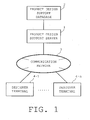
- FIG 1 illustrates the structure of the product design support system according to the embodiment.
- the product design support system comprises a product design support server 1, a product design support database 2, a communication network 3 and designer terminals 4 (4-1 to 4-n) connected via the communication network 3.
- the product design support server 1 is for doing various processes associated with the product design support system.
- the product design support server 1 comprises, for example, a CPU (Central Processing Unit) and a semiconductor memory, a magnetic disk recording device, etc.
- FIG 2 illustrates the structure of the product design support server 1.
- the product design support server 1 includes a communication control section 11, a process control section 12 and a data storage section 13. They are realized, for example, as the CPU of the product design support server 1 executes an operation program.
- the communication control section 11 which is comprised of, for example, a predetermined communication device, such as a rooter, connects the product design support server 1 to the communication network 3.
- the communication control section 11 transmits and receives various kinds of data (information) via the communication network 3.
- the process control section 12 performs communication via the communication control section 11, and processes various kinds of information. Further, the process control section 12 generates image data.
- the data storage section 13 which is comprised of a semiconductor memory, a magnetic disk recording or the like, records various kinds of information and programs.
- the product design support database 2 is a database (DB) to store various kinds of information associated with the product design support system.
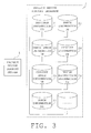
- FIG 3 illustrates the structure of the product design support database 2.
- the product design support database 2 comprises a designer information DB 21, a parts information DB 22, a parts image information DB 23, a circuit information DB 24, a circuit image information DB 25, a design restriction information DB 26, and an image information DB 27.
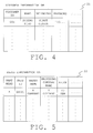
- the designer information DB 21 is a database to store information on a designer who designs a product (circuit) using the product design support system.
- a record is created for each designer ID, and a name, a belonging section, a password, etc. are stored in each record, as shown in FIG 4.
- the designer ID is identification information of a designer.
- the password is for a designer to log in the product design support system.
- the parts information DB 22 is a database to store information on parts information usable in a circuit.
- a record is created for each part classification (part name), and a part ID, a maker namer, a providing company name, a price, the specification of the part (spec), a part image number stored in the parts image information DB 23, etc. are stored in each record, as shown in FIG 5.
- the parts image information DB 23 is a database to store image data or the like of parts. Image data or the like in the parts image information DB 23 is stored in association with the part ID's stored in the parts information DB 22.
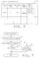
- the circuit information DB 24 is a database to store information on a designed circuit.
- a record is created for each circuit ID, and a circuit name, a designer ID, a maker name, the name of a part used, the layout position, etc. are stored in each record, as shown in FIG 6.
- the used part name, etc. all the parts used in the circuit are stored, and individual records created circuit ID by circuit ID become a list (parts table) of parts used in each circuit.
- information on restrictions determined at the time of designing the circuit i.e., unique restrictions on the circuit, is stored.
- unique restrictions on the circuit for example, there are shape restrictions, such as a height limitation on the circuit, and performance restrictions, such as a thermal limitation.
- circuits designed by different designers can be used in circuit design in a case where a designer draws a circuit diagram.
- the circuit image information DB 25 is a database to store image data or the like on a circuit stored in the circuit information DB 24. Image data or the like in the circuit image information DB 25 is stored in association with the circuit ID's stored in the circuit information DB 24.
- image data or the like in the circuit image information DB 25 is formed by the process control section 12 by image data or the like of used parts and layout positions stored in the circuit information DB 24 and parts stored in the parts image information DB 23. Therefore, when a designer changes a parts table through the circuit design process using the parts table to be discussed later (e.g., changes a part to be used in the circuit and its position), the process control section 12 changes information on associated image data or the like to be stored in the circuit image information DB 25.
- image data or the like in use is a CAD diagram (circuit diagram) prepared by CAD (Computer Aided Design), and all the parts to be used in the circuit and their positional relationship are illustrated.
- the design restriction information DB 26 is a database to store information on restrictions in circuit design.
- design restriction information DB 26 for example, design rules and wiring rules in circuit design are stored. It is therefore possible to perform a check routine to discriminate whether a designed circuit contains a logical miss or not as the product design support server 1 (process control section 12) discriminates whether the designed circuit corresponds to the information on the design restrictions stored in the design restriction information DB 26 or not.
- the design restriction information DB 26 information on unique circuit restrictions stored in the circuit information DB 24 is stored.
- the unique circuit restrictions about the circuit are determined in the circuit design process to be discussed later. It is therefore possible to discriminate whether the designed circuit meets unique circuit restrictions, such as restrictions on circuit implement, or not as the process control section 12 discriminates whether the designed circuit corresponds to information on the unique circuit restrictions stored in the design restriction information DB 26 or not.
- the image information DB 27 is a database to store information which forms various images to be displayed in individual processes to be discussed later, and stores images, various forms and the like of multifarious materials for generating those images.
- the communication network 3 is constituted by, for example, the Internet, LAN (Local Area Network), WAN (Wide Area Network), or the like.
- the communication network 3 when the communication network 3 is connected as the Internet to the designer terminals 4 of a plurality of companies, the system becomes a product design support system which is usable among the plural companies, and when the communication network 3 is an in-company LAN, the system becomes an in-company product design support system which connects a plurality of design sections in a company.
- the designer terminals 4 (4-1 to 4-n) are user terminals which uses the product design support system, and comprise a computer having a communication function, a portable terminal and the like.
- a browser is installed in the designer terminal 4.
- a CAD diagram is used for a circuit diagram and CAD is installed in the designer terminal 4.
- a product design support method using the product design support system constructed in the above manner will be described next.
- the product design support method using the product design support system there are circuit design using the circuit diagrams of a circuit designed already (existing circuit) and circuit design using a parts list (parts table) of an existing circuit. The following will describe pre-registration, log-in to the product design support system, circuit registration, and circuit design (circuit design using a circuit diagram, circuit design using a parts table) in order.
- a designer sends information, such as the name of the designer and the belonging section, to the product design support server 1 via the communication network 3 to the product design support server 1.
- the process control section 12 of the product design support server 1 issues a designer ID and a password, and sends the designer ID and the password to the designer terminal 4 by, for example, mail.
- the process control section 12 registers predetermined information, the designer ID and the password transmitted into the designer information DB 21.
- the designer can log in the product design support system.
- the following will describe a case where the designer logs in the product design support system.
- the process control section 12 of the product design support server 1 starts a process illustrated in the flowchart in FIG. 7.
- the process control section 12 reads information on a log-in screen as shown in FIG 8 (e.g., information in an HTML form) from the image information DB 27, sends it to the designer terminal 4, and displays the log-in screen on the product design support database 2 (step S1). Input fields to enter a log-in name and a password are laid out on the screen.
- a log-in screen as shown in FIG 8 (e.g., information in an HTML form) from the image information DB 27, sends it to the designer terminal 4, and displays the log-in screen on the product design support database 2 (step S1).
- Input fields to enter a log-in name and a password are laid out on the screen.
- the designer inputs a log-in name and a password on the screen, and clicks "Send".
- the entries are notified to the process control section 12 via the communication network 3.
- the process control section 12 discriminates whether the input information is registered in the designer information DB 21 or not (step S2).
- the process control section 12 When having discriminated that the input information is not registered in the designer information DB 21 (step S2; No), the process control section 12 sends information on an unillustrated registration guide screen (e.g., an HTML text) to the designer terminal 4, displays the registration guide screen on the designer terminal 4 (step S3), then terminates this process.
- an unillustrated registration guide screen e.g., an HTML text
- the process control section 12 When having discriminated that the input information is registered in the designer information DB 21 (step S2; Yes), on the other hand, the process control section 12 reads information on a menu screen (information in an HTML form) as shown in FIG. 9 from the image information DB 27, sends it to the designer terminal 4, displays the menu screen on the designer terminal 4 (step S4), then terminates this process.
- a menu screen information in an HTML form
- the menu screen has menu columns, such as "Register Parts” to register parts, “Register Circuit” to register a circuit, “Register Achievement” to register achievements about the characteristics of the circuit, “Design Circuit” to design the circuit, and so forth.
- the process control section 12 displays the menu screen shown in FIG 9 on the designer terminal 4 (step S11).
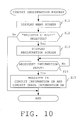
- the process control section 12 discriminates whether "Register Circuit" is selected on the menu screen or not (step S12). That is, it is discriminated whether the designer has clicked the "Register Circuit” on the menu screen or not.
- the process control section 12 terminates the process.
- the process control section 12 When having discriminated that the "Register Circuit" has been clicked (step S12; Yes), the process control section 12 reads information on a registration screen (information in an HTML form) as shown in FIG 11 from the image information DB 27, sends it to the designer terminal 4, and displays the registration screen on the designer terminal 4 (step S13).
- input fields to enter a circuit ID, a circuit name, a designer name, etc. are laid out on the registration screen.
- the designer inputs predetermined conditions in the input fields on the registration screen displayed on the designer terminal 4, and clicks the "Register” key.
- the designer inputs predetermined conditions in the input fields, and clicks the "Register” key.
- step S 14 discriminates whether the designer has input necessary information or not.
- step S 14 When having discriminated that the designer has input necessary information (step S 14; Yes), the process control section 12 registers the input information in the circuit information DB 24 and the circuit image information DB 25 (step S15), then terminals the process.
- Circuit design using a circuit diagram and circuit design using a parts table will be discussed in the embodiment.
- the process control section 12 displays a circuit design screen as shown in FIG. 12.
- menu columns such as "Use Circuit Diagram” to design a circuit using the circuit diagram of an existing circuit and "Use Parts Table” to design a circuit using a parts list (parts table) of an existing circuit.
- a menu column “New” to newly perform circuit design without using information on an existing circuit is laid out on the circuit design screen, so that circuit design can be performed newly without using information on an existing circuit.
- the designer can carry out circuit design using information on an existing circuit by clicking "Use Circuit Diagram” or "Use Parts Table” on the circuit design screen shown in FIG 12.
- the process control section 12 displays the circuit design screen as shown in FIG 12 on the designer terminal 4 (step S21).
- the process control section 12 discriminates whether "Use Circuit Diagram” is selected (clicked) on the circuit design screen or not (step S22). That is, it is discriminated whether the designer has clicked "Use Circuit Diagram” on the circuit design screen or not.
- the process control section 12 terminates the process.
- the process control section 12 When having discriminated that "Use Circuit Diagram" has been clicked (step S22; Yes), the process control section 12 reads information on a retrieval screen (information in an HTML form) as shown in FIG 14 from the image information DB 27, sends it to the designer terminal 4, and displays the retrieval screen on the designer terminal 4 (step S23).
- the retrieval screen has input fields for retrieval keys, such as a circuit name, a maker name and the name of a part to be used, laid out thereon.
- the designer inputs predetermined conditions in the input fields on the retrieval screen displayed on the designer terminal 4, and clicks the "Retrieve" key.
- the process control section 12 extracts a circuit corresponding to the predetermined conditions from circuits registered in the circuit information DB 24, sends the extraction results to the designer terminal 4, and displays the extraction results on the designer terminal 4. Accordingly, the designer can retrieve (specify) a circuit (diagram) to be used.
- the designer can specify not only one circuit diagram, but can specify a plurality of circuit diagrams. As a plurality of circuit diagrams are specified, it is possible to perform circuit design with a combination of specified circuit diagrams.
- the process control section 12 discriminates whether the designer has specified a circuit diagram or not (step S24).
- the process control section 12 reads the specified circuit diagram from the circuit image information DB 25, sends it to the designer terminal 4, and displays the specified circuit diagram on the designer terminal 4 (step S25).
- the designer can carry out circuit design using the circuit diagram displayed on the designer terminal 4.
- the circuit diagram displayed on the designer terminal 4 is a CAD diagram drawn using CAD. Accordingly, using CAD, the designer can carry out circuit design by making an addition or a change to the circuit diagram displayed on the designer terminal 4.
- the process control section 12 changes information on parts used in the corresponding circuit, layout positions thereof, and the like.
- the process control section 12 adds the part C to the corresponding parts table (circuit information DB 24) as shown in FIG. 15B.
- circuit image information DB 25 and the circuit information DB 24 and information on the circuit diagrams is collectively managed by the product design support server 1 (process control section 12), the designer can use the circuit diagrams efficiently. Further, circuit design can be carried out using circuit diagrams already designed, so that designing a circuit can be made easier.
- the process control section 12 reads information on unique restrictions on the specified circuit from the circuit information DB 24, sends it to the designer terminal 4, and displays the information on the unique restrictions on the designer terminal 4 (step S26). The designer checks if the displayed restrictions are correct, and input correct restrictions when they are wrong. Accordingly, information on unique circuit restrictions in the present circuit design is determined (step S27).
- the process control section 12 discriminates whether the designer has done circuit design or not, i.e., whether the circuit diagram is changed or not (step S28).
- the process control section 12 discriminates whether the changed (designed) circuit corresponds to the information on design restrictions stored in the design restriction information DB 26 or not (step S29). That is, the process control section 12 discriminates whether the changed circuit diagram contains a logical miss or not (check routine), and discriminates whether it corresponds to unique restrictions of the circuit diagram itself or not.
- step S29 When having discriminated that it corresponds to design restrictions (step S29; Yes), the process control section 12 displays (sends) on the designer terminal 4 information to the effect that it corresponds to design restrictions to inform the designer that there is a logical miss, returns to step S28 and requests the designer to perform circuit design again.
- design restriction information DB 26 information on design rules and wiring rules in circuit design is stored in the design restriction information DB 26. Therefore, it is possible to perform a check routine to discriminate whether the designed circuit contains a logical miss or not by discriminating whether the designed circuit corresponds to information on design restrictions stored in the design restriction information DB 26 or not. This makes it easier to do a work of checking that the designed circuit does not contain a logical miss, and makes it easier to design the circuit. Particularly, the work of determining the optimal positions of the parts to be used in the circuit becomes easier.
- circuit information DB 24 information on unique restrictions of a circuit stored in the circuit information DB 24 is stored in the design restriction information DB 26. This makes it possible to discriminate whether unique restrictions of the circuit to be designed are met or not. Therefore, designing of the circuit becomes easier.
- step S29 When having discriminated that it does not correspond to design restrictions (step S29; No), information on the CAD diagram (image data of the circuit) is registered in the circuit image information DB 25, information on the designed circuit is registered in the circuit information DB 24 (step S30), then the process is terminated.
- the process control section 12 displays the circuit design screen as shown in FIG 12 on the designer terminal 4 (step S31).
- the process control section 12 discriminates whether "Use Parts Table” is selected (clicked) on the circuit design screen or not (step S32). That is, it is discriminated whether the designer has clicked "Use Parts Table” on the circuit design screen or not.
- step S32 When having discriminated that "Use Parts Table” has not been clicked (step S32; No), the process control section 12 terminates the process.
- the process control section 12 When having discriminated that "Use Parts Table" has been clicked (step S32; Yes), the process control section 12 reads information on a retrieval screen (information in an HTML form) as shown in FIG. 14 from the image information DB 27, sends it to the designer terminal 4, and displays the retrieval screen on the designer terminal 4 (step S33).
- the process control section 12 extracts a circuit corresponding to the predetermined conditions from circuits registered in the circuit information DB 24, sends the extraction results to the designer terminal 4, and displays the extraction results on the designer terminal 4. Accordingly, the designer can retrieve (specify) the parts table of a circuit to be used.
- the process control section 12 discriminates whether the designer has specified a parts table or not (step S34).
- the process control section 12 reads the specified parts table from the circuit information DB 24, sends it to the designer terminal 4, and displays the specified parts table on the designer terminal 4 (step S35).
- the designer can carry out circuit design, such as changing parts from the parts table displayed on the designer terminal 4 using the existing parts table.
- circuit design such as changing parts from the parts table displayed on the designer terminal 4 using the existing parts table.
- the process control section 12 changes information on image data or the like of the corresponding circuit.
- circuit information DB 24 As information on existing parts tables is stored in the circuit information DB 24, and information on the parts tables is collectively managed by the product design support server 1 (process control section 12), the designer can use the parts tables efficiently. Further, circuit design can be carried out using parts tables already designed, so that designing a circuit can be made easier.
- the process control section 12 reads information on unique restrictions on the specified circuit from the circuit information DB 24, sends it to the designer terminal 4, and displays the information on the unique restrictions on the designer terminal 4 (step S36). The designer checks if the displayed restrictions are correct, and input correct restrictions when they are wrong. Accordingly, information on unique circuit restrictions in the present circuit design is determined (step S37).
- step S38 the process control section 12 discriminates whether the designer has done circuit design or not, i.e., whether the parts table is changed or not.
- step S38 the process control section 12 discriminates whether the changed (designed) circuit corresponds to the information on design restrictions or not (step S39).
- step S39 When having discriminated that it corresponds to design restrictions (step S39; Yes), the process control section 12 displays (sends) on the designer terminal 4 information to the effect that it corresponds to design restrictions to inform the designer that there is a logical miss, returns to step S38 and requests the designer to perform circuit design again.
- the process control section 12 displays (sends) on the designer terminal 4 information to the effect that it corresponds to design restrictions to inform the designer that there is a logical miss, returns to step S38 and requests the designer to perform circuit design again.
- the designed circuit corresponds to information on design restrictions stored in the design restriction information DB 26 or not, therefore, it is possible to discriminate whether the designed circuit diagram contains a logical miss or not or unique circuit restrictions are met or not, making designing of a circuit easier.
- step S39 When having discriminated that it does not correspond to design restrictions (step S39; No), information on the designed circuit is registered in the circuit information DB 24, information on image data or the like of the drawn circuit diagram is registered in the circuit image information DB 25 (step S40), then the process is terminated.
- the process control section 12 displays the circuit design screen shown in FIG 12 on the designer terminal 4 (step S61).
- the process control section 12 discriminates whether "New" is selected (clicked) on the circuit design screen or not (step S62). That is, it is discriminated whether the designer has clicked "New” on the circuit design screen or not.
- step S62 When having discriminated that "New" has not been clicked (step S62; No), the process control section 12 terminates the process.
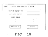
- the process control section 12 When having discriminated that "New" has been clicked (step S62; Yes), the process control section 12 reads information on a specification designating screen (information in an HTML form) as shown in FIG 18 from the image information DB 27, sends it to the designer terminal 4, and displays the specification designating screen on the designer terminal 4 (step S63).
- the specification designating screen has input fields for the specification (spec), such as the functions of the circuit and the circuit characteristics, laid out thereon.
- spec specification
- circuit functions possible such as logical operations, power supply, amplification and modulation.
- circuit characteristics possible such as the input v.s. output characteristics, formulae showing the contents of logical operations, the delay time, consumed power and other restriction conditions.
- the process control section 12 extracts a circuit having functions similar to the functions designated by the designer from, for example, circuits registered in the circuit information DB 24 (step S64).
- the functions designated by the designer are realized by the combination of plural circuits, corresponding plural circuits may be extracted.
- the process control section 12 searches the parts information DB 22 or the circuit information DB 24 to further extract candidates for parts to be constituting elements of the circuit in place of the parts constituting the previously extracted circuit, based on the circuit characteristics designated by the designer or other specifications.
- the process control section 12 may extract not only possible substitute parts for the parts, but also a circuit substitutable for parts, or parts or a circuit which is substitutable for a part of the previously extracted circuit.
- the process control section 12 simulate an operation for discriminating whether the extracted circuit and various circuits acquired by replacing the parts of the circuit with various candidates are compatible with the specification designated by the designer, and specifies a circuit which is compatible with the specification designated by the designer based on the computed simulation results (step S65).
- a circuit which achieves the specification designated by the designer with the greatest allowance e.g., when consumed power is designated, a circuit with the lowest consumed power among circuits which satisfy all the specifications other than the consumed power
- a circuit which achieves the specification closest to the one designated by the designer e.g., a circuit with the minimum width exceeding the designated consumed power
- the process control section 12 creates data including image data as data representing the specified circuit, and sends it to the designer terminal 4 (step S66). Then designer terminal 4 displays the circuit represented by the data, the designer terminal 4 may display the parts table of the circuit.
- the designer can allow the product design support system to generate a final circuit to be obtained or its interim circuit before editing himself, and can carry out circuit design using the circuit (and/or the parts table of the circuit) whose data has been generated at step S66.
- the process control section 12 discriminates whether or not circuit design using the circuit whose data has been sent at step S66 is carried out and the circuit or the parts table of the circuit has been changed (steps S28 and S38). When it is discriminated that the circuit diagram is changed, the processing at and after the step S29 is executed. When it is discriminated that the parts table is changed, the processing at and after the step S39 is executed. It is to be noted that at steps S29 and S39, the process control section 12 performs processing considering that information on the circuit characteristics or the like written in the input fields on the specification designating screen by the designer as information on the unique restrictions of the circuit diagram. At steps S30 and S40, information on the circuit characteristics or the like written in the input fields on the specification designating screen by the designer is stored in the circuit information DB 24 as information on the unique restrictions of the circuit diagram.
- circuit image information DB 25 and the circuit information DB 24 and information on the circuits is collectively managed by the product design support server 1, the designer can use the existing circuit diagrams or parts tables efficiently. Circuit design can be performed using the existing circuit diagrams or parts tables, making it possible to do circuit design easier.
- circuit design becomes easier.
- information on design rules and wiring rules in circuit design is stored in the design restriction information DB 26, so that it is possible to perform a check routine to discriminate whether the designed circuit contains a logical miss or not by discriminating whether the designed circuit corresponds to information on design restrictions stored in the design restriction information DB 26 or not.
- This makes it easier to do a work of checking that the designed circuit does not contain a logical miss, and makes it easier to design the circuit.
- the work of determining the optimal positions of the parts to be used in the circuit becomes easier.
- information on unique restrictions of a circuit stored in the circuit information DB 24 is stored in the design restriction information DB 26. This makes it possible to discriminate whether unique restrictions of the circuit to be designed are met or not. Therefore, designing of the circuit becomes easier.
- the invention is not limited to the embodiment, but can be modified and adapted in various forms.
- the system configuration and the screen structure can be changed as needed.
- the processing procedures or the like can be changed as needed if substantially the same functions can be achieved.
- circuit information DB 24 information on unique circuit restrictions may not be stored in the circuit information DB 24.
- the design restriction information DB 26 may not be provided in the product design support database 2 and a check routine to discriminate whether the designed circuit contains a logical miss or not may not be executed. As information on circuits is collectively managed by the product design support server 1 even in those cases, the designer can efficiently use existing circuit diagrams or parts tables.
- the target for design support according to the invention has only to be a product comprising a plurality of parts, and is not limited to a circuit.
- the product design support system according to the embodiment of the invention can be achieved by not only an exclusive system, but also by using an ordinary computer system.
- the product design support system that executes the above-described processes can be constructed by installing programs for executing the above-described processes into a general-purpose computer from a recording medium (flexible disk, CD-R or the like) where the programs are stored.
- Means for supplying the programs is arbitrary. They may be supplied not only via a predetermined recording medium as mentioned above, but also via a communication circuit, a communication network, a communication system or the like, for example:
- the program may be presented on the bulletin board system (BBS) and may be superimposed on a carrier wave over a network. Then, the above-described processes can be executed by activating the program provided this way and running the program under the control of the OS in the way other application programs are run.
- BSS bulletin board system
Landscapes
- Engineering & Computer Science (AREA)
- Physics & Mathematics (AREA)
- Theoretical Computer Science (AREA)
- Computer Hardware Design (AREA)
- Evolutionary Computation (AREA)
- Geometry (AREA)
- General Engineering & Computer Science (AREA)
- General Physics & Mathematics (AREA)
- Management, Administration, Business Operations System, And Electronic Commerce (AREA)
Applications Claiming Priority (3)
| Application Number | Priority Date | Filing Date | Title |
|---|---|---|---|
| JP2002378108 | 2002-12-26 | ||
| JP2002378108 | 2002-12-26 | ||
| PCT/JP2003/016885 WO2004059537A1 (ja) | 2002-12-26 | 2003-12-26 | 製品設計支援システム、製品設計支援方法及びプログラム |
Publications (1)
| Publication Number | Publication Date |
|---|---|
| EP1577800A1 true EP1577800A1 (de) | 2005-09-21 |
Family
ID=32677417
Family Applications (1)
| Application Number | Title | Priority Date | Filing Date |
|---|---|---|---|
| EP03782919A Withdrawn EP1577800A1 (de) | 2002-12-26 | 2003-12-26 | Produktdesignhilfssystem, produktdesignhilfsverfahren und programm |
Country Status (5)
| Country | Link |
|---|---|
| US (1) | US7502721B2 (de) |
| EP (1) | EP1577800A1 (de) |
| KR (1) | KR100723323B1 (de) |
| CN (1) | CN100449552C (de) |
| WO (1) | WO2004059537A1 (de) |
Families Citing this family (10)
| Publication number | Priority date | Publication date | Assignee | Title |
|---|---|---|---|---|
| CN100424708C (zh) * | 2005-03-24 | 2008-10-08 | 英业达股份有限公司 | 具累积模块化设计经验的系统及其方法 |
| JP4822863B2 (ja) * | 2006-02-08 | 2011-11-24 | 富士通株式会社 | 数値解析データ作成方法及び装置並びにプログラム及び記憶媒体 |
| JP5454216B2 (ja) * | 2010-02-23 | 2014-03-26 | 富士通株式会社 | 電子装置の設計装置、電子装置の設計プログラム、及び電子装置の設計方法 |
| CN101901490B (zh) * | 2010-07-15 | 2011-12-07 | 北京信息科技大学 | 生成信号调理电路图像的系统 |
| KR101409666B1 (ko) * | 2013-03-19 | 2014-06-18 | 한국생산기술연구원 | 사용자 맞춤형 개인 이동 수단 제공 시스템 및 방법 |
| KR20140119305A (ko) * | 2013-03-28 | 2014-10-10 | 삼성전자주식회사 | 모바일 어플리케이션 디자인 및 시뮬레이션 기능을 제공하는 스마트 디자인 시스템, 이를 포함하는 비즈니스 모델 및 스마트 디자인 시스템의 동작방법 |
| JP6155404B2 (ja) * | 2015-03-05 | 2017-06-28 | 株式会社ミスミ | 設計支援方法 |
| JP7424292B2 (ja) | 2018-08-31 | 2024-01-30 | 株式会社Gsユアサ | 開発支援装置、端末装置、開発支援方法、及びコンピュータプログラム |
| KR102593877B1 (ko) * | 2023-06-30 | 2023-10-25 | 에코케미컬 주식회사 | 인공지능 기반 재고 관리 시스템 |
| KR102578734B1 (ko) * | 2023-07-10 | 2023-09-13 | 이상호 | 산업용 자동화 장비의 용도 및 설계 정보를 기반으로 한 부품 정보의 제공, 주문 처리 및 재고 관리 시스템 |
Family Cites Families (10)
| Publication number | Priority date | Publication date | Assignee | Title |
|---|---|---|---|---|
| JPH08314996A (ja) * | 1995-05-18 | 1996-11-29 | Toshiba Corp | Cadライブラリ管理装置 |
| EP0833264B1 (de) * | 1996-09-30 | 2004-12-01 | Nippon Telegraph And Telephone Corporation | Entwurfssystem und -verfahren für optische Schaltungen |
| US5812130A (en) * | 1996-12-06 | 1998-09-22 | International Business Machines Corporation | Data management system and method for concurrent engineering |
| US7071952B1 (en) * | 1998-11-30 | 2006-07-04 | Actcon Control Ab | Method for inserting objects into a working area in a computer application |
| US6957186B1 (en) * | 1999-05-27 | 2005-10-18 | Accenture Llp | System method and article of manufacture for building, managing, and supporting various components of a system |
| JP3954253B2 (ja) * | 1999-11-01 | 2007-08-08 | 富士通株式会社 | Lsiフロアプラン決定装置及び方法並びにプログラム記録媒体 |
| JP2002099583A (ja) * | 2000-07-19 | 2002-04-05 | Toshiba Tec Corp | 回路設計支援方法及び回路設計支援システム並びにプログラムを記録したコンピュータ読み取り可能な記録媒体 |
| JP4354131B2 (ja) | 2000-07-21 | 2009-10-28 | 株式会社リコー | 部品管理システム及び部品管理方法 |
| JP2002157294A (ja) * | 2000-11-17 | 2002-05-31 | Sanyo Electric Co Ltd | 集積回路設計のシミュレーション方法およびシミュレーションシステム |
| JP2002157504A (ja) * | 2000-11-17 | 2002-05-31 | Ricoh Co Ltd | 設計支援システム |
-
2003
- 2003-12-26 EP EP03782919A patent/EP1577800A1/de not_active Withdrawn
- 2003-12-26 US US10/540,391 patent/US7502721B2/en not_active Expired - Fee Related
- 2003-12-26 CN CNB2003801099141A patent/CN100449552C/zh not_active Expired - Fee Related
- 2003-12-26 WO PCT/JP2003/016885 patent/WO2004059537A1/ja not_active Ceased
- 2003-12-26 KR KR1020057012041A patent/KR100723323B1/ko not_active Expired - Fee Related
Non-Patent Citations (1)
| Title |
|---|
| See references of WO2004059537A1 * |
Also Published As
| Publication number | Publication date |
|---|---|
| KR20050094415A (ko) | 2005-09-27 |
| US20060155760A1 (en) | 2006-07-13 |
| WO2004059537A1 (ja) | 2004-07-15 |
| CN1754170A (zh) | 2006-03-29 |
| US7502721B2 (en) | 2009-03-10 |
| CN100449552C (zh) | 2009-01-07 |
| KR100723323B1 (ko) | 2007-05-31 |
Similar Documents
| Publication | Publication Date | Title |
|---|---|---|
| JP4898090B2 (ja) | 設計、調達及び製造の協働のためのシステム及び方法 | |
| US6594799B1 (en) | Method and system for facilitating electronic circuit and chip design using remotely located resources | |
| US6851094B1 (en) | Automated method and system for selecting and procuring electronic components used in circuit and chip designs | |
| US20020156757A1 (en) | Electronic product design system | |
| JP2005520246A (ja) | ネットワーク基盤部品管理システムのためのシステム、方法およびコンピュータプログラム製品 | |
| US20040107214A1 (en) | Customized document portfolio system integrating IP libraries and technology documents | |
| US7502721B2 (en) | Product design support system, product design support method, and program | |
| CN111427577A (zh) | 代码处理方法、装置及服务器 | |
| JP7587781B2 (ja) | プログラム、方法、情報処理装置、及びシステム | |
| US20060253776A1 (en) | Information processing device, information processing system, information processing method, information processing program and recording medium recording the informaiton processing program | |
| US7467122B2 (en) | System for aiding the design of product configuration | |
| JP4084229B2 (ja) | 製品データ管理システム及びプログラム | |
| EP2088523A1 (de) | Vorrichtung zur Unterstützung einer Analyse, Verfahren zur Unterstützung einer Analyse und Programm zur Unterstützung einer Analyse | |
| US20010039536A1 (en) | Cost data management system, method of managing cost data, and recording medium | |
| KR101602940B1 (ko) | 컴포넌트 구조를 이용하여 사이트의 제작을 지원하는 사이트 관리 방법 및 시스템 | |
| JP4648194B2 (ja) | プリント基板設計指示支援方法およびその装置 | |
| JP2004220600A (ja) | 製品設計支援システム、製品設計支援方法及びプログラム | |
| US20010032222A1 (en) | System, method and computer accessible storage medium, for creating and editing structured parts list | |
| JP3939550B2 (ja) | オブジェクト整合管理方法及びシステム | |
| JP2009176053A (ja) | 解析支援装置、解析支援方法および解析支援プログラム | |
| JP2003016072A (ja) | 部品検索システム及び部品検索方法並びに部品検索プログラム | |
| JP4918278B2 (ja) | 顧客向けlsiデータ提供システム | |
| US20020083402A1 (en) | Method and system for simulating integrated circuit designs | |
| JP2009176051A (ja) | 解析支援装置、解析支援方法および解析支援プログラム | |
| JP2001297113A (ja) | 部品構成作成編集装置と部品構成作成編集方法と部品構成作成編集処理プログラムを記録したコンピュータ読み取り可能な記録媒体 |
Legal Events
| Date | Code | Title | Description |
|---|---|---|---|
| PUAI | Public reference made under article 153(3) epc to a published international application that has entered the european phase |
Free format text: ORIGINAL CODE: 0009012 |
|
| 17P | Request for examination filed |
Effective date: 20050624 |
|
| AK | Designated contracting states |
Kind code of ref document: A1 Designated state(s): AT BE BG CH CY CZ DE DK EE ES FI FR GB GR HU IE IT LI LU MC NL PT RO SE SI SK TR |
|
| AX | Request for extension of the european patent |
Extension state: AL LT LV MK |
|
| DAX | Request for extension of the european patent (deleted) | ||
| RBV | Designated contracting states (corrected) |
Designated state(s): DE ES GB |
|
| STAA | Information on the status of an ep patent application or granted ep patent |
Free format text: STATUS: THE APPLICATION HAS BEEN WITHDRAWN |
|
| 18W | Application withdrawn |
Effective date: 20091222 |