EP1577696A2 - Commutateur optique - Google Patents
Commutateur optique Download PDFInfo
- Publication number
- EP1577696A2 EP1577696A2 EP05013442A EP05013442A EP1577696A2 EP 1577696 A2 EP1577696 A2 EP 1577696A2 EP 05013442 A EP05013442 A EP 05013442A EP 05013442 A EP05013442 A EP 05013442A EP 1577696 A2 EP1577696 A2 EP 1577696A2
- Authority
- EP
- European Patent Office
- Prior art keywords
- optical switch
- input
- moving member
- block
- blocks
- Prior art date
- Legal status (The legal status is an assumption and is not a legal conclusion. Google has not performed a legal analysis and makes no representation as to the accuracy of the status listed.)
- Withdrawn
Links
Images




Classifications
-
- G—PHYSICS
- G02—OPTICS
- G02B—OPTICAL ELEMENTS, SYSTEMS OR APPARATUS
- G02B6/00—Light guides; Structural details of arrangements comprising light guides and other optical elements, e.g. couplings
- G02B6/24—Coupling light guides
- G02B6/26—Optical coupling means
- G02B6/35—Optical coupling means having switching means
- G02B6/3564—Mechanical details of the actuation mechanism associated with the moving element or mounting mechanism details
- G02B6/358—Latching of the moving element, i.e. maintaining or holding the moving element in place once operation has been performed; includes a mechanically bistable system
-
- G—PHYSICS
- G02—OPTICS
- G02B—OPTICAL ELEMENTS, SYSTEMS OR APPARATUS
- G02B26/00—Optical devices or arrangements for the control of light using movable or deformable optical elements
- G02B26/08—Optical devices or arrangements for the control of light using movable or deformable optical elements for controlling the direction of light
- G02B26/0816—Optical devices or arrangements for the control of light using movable or deformable optical elements for controlling the direction of light by means of one or more reflecting elements
- G02B26/0833—Optical devices or arrangements for the control of light using movable or deformable optical elements for controlling the direction of light by means of one or more reflecting elements the reflecting element being a micromechanical device, e.g. a MEMS mirror, DMD
- G02B26/085—Optical devices or arrangements for the control of light using movable or deformable optical elements for controlling the direction of light by means of one or more reflecting elements the reflecting element being a micromechanical device, e.g. a MEMS mirror, DMD the reflecting means being moved or deformed by electromagnetic means
-
- G—PHYSICS
- G02—OPTICS
- G02B—OPTICAL ELEMENTS, SYSTEMS OR APPARATUS
- G02B7/00—Mountings, adjusting means, or light-tight connections, for optical elements
- G02B7/18—Mountings, adjusting means, or light-tight connections, for optical elements for prisms; for mirrors
- G02B7/182—Mountings, adjusting means, or light-tight connections, for optical elements for prisms; for mirrors for mirrors
- G02B7/1822—Mountings, adjusting means, or light-tight connections, for optical elements for prisms; for mirrors for mirrors comprising means for aligning the optical axis
- G02B7/1827—Motorised alignment
- G02B7/1828—Motorised alignment using magnetic means
-
- H—ELECTRICITY
- H04—ELECTRIC COMMUNICATION TECHNIQUE
- H04Q—SELECTING
- H04Q11/00—Selecting arrangements for multiplex systems
- H04Q11/0001—Selecting arrangements for multiplex systems using optical switching
- H04Q11/0005—Switch and router aspects
-
- G—PHYSICS
- G02—OPTICS
- G02B—OPTICAL ELEMENTS, SYSTEMS OR APPARATUS
- G02B6/00—Light guides; Structural details of arrangements comprising light guides and other optical elements, e.g. couplings
- G02B6/24—Coupling light guides
- G02B6/26—Optical coupling means
- G02B6/35—Optical coupling means having switching means
- G02B6/351—Optical coupling means having switching means involving stationary waveguides with moving interposed optical elements
- G02B6/3512—Optical coupling means having switching means involving stationary waveguides with moving interposed optical elements the optical element being reflective, e.g. mirror
- G02B6/3514—Optical coupling means having switching means involving stationary waveguides with moving interposed optical elements the optical element being reflective, e.g. mirror the reflective optical element moving along a line so as to translate into and out of the beam path, i.e. across the beam path
-
- G—PHYSICS
- G02—OPTICS
- G02B—OPTICAL ELEMENTS, SYSTEMS OR APPARATUS
- G02B6/00—Light guides; Structural details of arrangements comprising light guides and other optical elements, e.g. couplings
- G02B6/24—Coupling light guides
- G02B6/26—Optical coupling means
- G02B6/35—Optical coupling means having switching means
- G02B6/354—Switching arrangements, i.e. number of input/output ports and interconnection types
- G02B6/3544—2D constellations, i.e. with switching elements and switched beams located in a plane
- G02B6/3546—NxM switch, i.e. a regular array of switches elements of matrix type constellation
-
- G—PHYSICS
- G02—OPTICS
- G02B—OPTICAL ELEMENTS, SYSTEMS OR APPARATUS
- G02B6/00—Light guides; Structural details of arrangements comprising light guides and other optical elements, e.g. couplings
- G02B6/24—Coupling light guides
- G02B6/26—Optical coupling means
- G02B6/35—Optical coupling means having switching means
- G02B6/354—Switching arrangements, i.e. number of input/output ports and interconnection types
- G02B6/3544—2D constellations, i.e. with switching elements and switched beams located in a plane
- G02B6/3548—1xN switch, i.e. one input and a selectable single output of N possible outputs
- G02B6/355—1x2 switch, i.e. one input and a selectable single output of two possible outputs
-
- G—PHYSICS
- G02—OPTICS
- G02B—OPTICAL ELEMENTS, SYSTEMS OR APPARATUS
- G02B6/00—Light guides; Structural details of arrangements comprising light guides and other optical elements, e.g. couplings
- G02B6/24—Coupling light guides
- G02B6/26—Optical coupling means
- G02B6/35—Optical coupling means having switching means
- G02B6/3564—Mechanical details of the actuation mechanism associated with the moving element or mounting mechanism details
- G02B6/3568—Mechanical details of the actuation mechanism associated with the moving element or mounting mechanism details characterised by the actuating force
- G02B6/3572—Magnetic force
-
- H—ELECTRICITY
- H04—ELECTRIC COMMUNICATION TECHNIQUE
- H04Q—SELECTING
- H04Q11/00—Selecting arrangements for multiplex systems
- H04Q11/0001—Selecting arrangements for multiplex systems using optical switching
- H04Q11/0005—Switch and router aspects
- H04Q2011/0007—Construction
- H04Q2011/0024—Construction using space switching
-
- H—ELECTRICITY
- H04—ELECTRIC COMMUNICATION TECHNIQUE
- H04Q—SELECTING
- H04Q11/00—Selecting arrangements for multiplex systems
- H04Q11/0001—Selecting arrangements for multiplex systems using optical switching
- H04Q11/0005—Switch and router aspects
- H04Q2011/0007—Construction
- H04Q2011/0026—Construction using free space propagation (e.g. lenses, mirrors)
- H04Q2011/003—Construction using free space propagation (e.g. lenses, mirrors) using switches based on microelectro-mechanical systems [MEMS]
-
- H—ELECTRICITY
- H04—ELECTRIC COMMUNICATION TECHNIQUE
- H04Q—SELECTING
- H04Q11/00—Selecting arrangements for multiplex systems
- H04Q11/0001—Selecting arrangements for multiplex systems using optical switching
- H04Q11/0005—Switch and router aspects
- H04Q2011/0052—Interconnection of switches
- H04Q2011/0058—Crossbar; Matrix
Definitions
- the present invention relates to an optical switch used for an optical communication network, and in particular to an optical switch capable of simplifying an assembly process, reducing a size thereof and minimizing power consumption.
- an interface connecting a subscriber with a relay or another subscriber is constructed as an optical connector module having an optical switch, a photo diode and a laser diode, etc.
- Optical communication network data interface nowadays put to practical use consists of optical fiber as a transmission line; a fiber optic connector for connecting subscribers with each other; optical switches and an optic transmitter having a laser diode, etc.
- optical communication network data interface because precision processing and lots of assembly process are required, it is expensive.
- the optical switch as the core part of the optical data interface, because a switching function is performed by arranging an optical axis by moving the front end of input and output side optical fibers mechanically, it has problems such as miniaturization intricacy, high power consumption and expensive price.
- Figure 1 is a block diagram illustrating an optical switch in accordance with the conventional art.
- the conventional optical switch includes input blocks 102, 104 in which light is incident; output blocks 106, 108 for transmitting/outputting input light from the input blocks 102, 104; a reflector 110 for performing a switching operation by reflecting input light from the input blocks 102 104; and a driving unit for reflecting or passing input light from the input blocks 102, 104 by operating the reflector 110.
- the first input block 102 and the second input block 104 are arranged to be at right angle to each other, the first output block 106 and the second output block 108 are arranged to be at right angle to each other, herein, the first input block 102 and the first output block are arranged on the same plane, and the second input block 104 and the second output block 108 are arranged on the same plane.
- a straight line connecting the first input block 102 with the first output block 106 and a straight line connecting the second input block 104 with the second output block 108 cross each other at the center of the reflector 110, and the reflector 110 is moved to a reflection position or a non-reflection position according to the operation of the driving unit.
- an angle between the input light 120, 124 and the reflected light 122, 126 is determined by an angle between the input light 120, 124 and the reflector 110. Accordingly, the input block 102, 104 is arranged to be at right angle to the output block 106, 108, an angle between the input light 120, 124 and the reflector 110 is 45°, an angle between the input light 120, 124 and the reflector 122, 126 is 90°.
- the reflector 10 when the reflector 10 is moved to a position out of a light path of the reflector 10, as depicted in Figure 2, the input light 120 from the first input block 102 is directly transferred to the first output block 106, and the input light 124 from the second input block 104 is directly transferred to the second output block 108.
- Figure 3 illustrates a reflector drive unit in accordance wit the conventional art.
- the conventional drive unit includes a substrate 132 having a coil 130 wound on the top surface in the circumferential direction; supporting protrusions 134 projected from the surface of the substrate 132 so as to have a certain height at regular intervals; a spring 136 for generating an elastic force by being supported between the supporting protrusions 134; a moving member 138 in which one end is fixed to the spring 136, the other end has a free-end shape and is connected to the reflector 110; and a magnet 140 mounted on the moving member 138 so as to be operated up and down by being mutually operated with the coil 130 when power is applied to the coil 130.
- the coil 130 is patterned as a shape wound on the surface of the substrate 132, and power connectors 142, 144 in which power is applied are respectively formed at both ends of the coil 130.
- the magnet 140 is arranged at the center of the substrate 132, when power is applied to the coil 130, it is operated in the upper direction or the lower direction by a magnetic field formed between the coil 130 and the magnet 140, and accordingly the moving member 138 on which the magnet 140 is mounted is rotated.
- the drive unit When power is applied to the coil 130 through the power connectors 142, 144, by the mutual operation of the coil 130 and the magnet 140, the magnet 140 is operated in the upper direction and the lower direction. According to that, while the free end of the moving member 138 on which the magnet 140 is fixed is rotated in the upper direction or the lower direction centering around a point fixed to the spring 136, the reflector 110 is driven to a position at which the input light 120, 124 is not reflected.
- the moving member when power applied to the coil 130 is cut off, by the elastic force of the spring 136, the moving member is returned to an initial position, herein, the reflector 110 is located on a position at which the input light 120, 124 is reflected.
- the input block 102, 104 is at right angle to the output block 106, 108, a light input angle and a light output angle are respectively 90°, assembly process and packaging process for integrating parts such as optical fiber, etc. to an optical device fabricated by micro-machining may be intricate.
- the first input block 102 and the second input block 104 are horizontally arranged on a surface of a package main body 150, and the first output block 106 and the second output block 108 are horizontally arranged on the opposite surface.
- optical fiber arranged at right angle has to be horizontally arranged to reduce a size of a whole package, however, it is difficult due to radius curvature of optical fiber itself.
- an object of the present invention to provide an optical switch capable of simplifying an assembly process and a package process and reducing a size of an optical switch package by improving an arranging method of an input block and an output block.
- an optical switch includes an input block in which light is incident; an output block to which input light from the input block is transferred; and a reflector for performing a switching operation by reflecting input light from the input block; wherein the input block and the output block are arranged so as to make input light from the input block and reflected light reflected by the reflector and transferred to the output block have an acute angle less than 90 degrees.
- the input block consists of a first input block and a second input block arranged to have an obtuse angle greater than 90 degrees therebetween
- the output block consists of a first output block and a second output block arranged to have an obtuse angle greater than 90 degrees therebetween.
- the first input block and the second output block are arranged at a side of a package main body to have an acute angle therebetween, and the second input block and the first output block are arranged at the other side of the package main body to have an acute angle therebetween.
- Plural first input blocks and plural second input blocks are arranged to have an obtuse angle greater than 90 degrees therebetween, plural first output blocks and plural second output blocks are arranged to have an obtuse angle greater than 90 degrees, and the reflector is arranged at all positions at which a straight line between the first input blocks and the first output blocks and a straight line between the second input blocks and the second output blocks cross each other.
- An optical switch includes an input block in which light is incident; an output block to which input light from the input block is transferred; and a reflector for performing a switching operation by reflecting input light from the input block; wherein the input block and the output block are arranged so as to make input light from the input block and reflected light reflected by the reflector and transferred to the output block have an obtuse angle greater than 90 degrees.
- the optical switch further includes a drive unit for moving the reflector to a direction reflecting input light and a direction not reflecting input light.
- the drive unit includes a moving member connected with the reflector to move the reflector; a spring for supporting the moving member and making the moving member return to an initial state; and an electromagnetic force generator for moving the moving member when a current is applied and maintaining the moved state of the moving member when a current is not continually applied.
- the electromagnetic force generator includes a core arranged at right angles to the free end of the moving member on which the magnet is adhered, made of a ferromagnetic material in order to rotate the moving member on which the magnet is fixed by generating a magnetic force when current is applied to a coil and maintain the moving member-rotated state by maintaining an electromagnetic force when the current applied to the coil is cut off; a coil wound around the core to apply a current.
- Figure 5 illustrates a construction of an optical switch in accordance with a first embodiment of the present invention.
- the optical switch in accordance with the first embodiment of the present invention includes input blocks 10, 12 in which light is incident; output blocks 14, 16 to which input light form the input blocks 10, 12 is transferred; a reflector 18 for performing a switching operation by reflecting input light from the input blocks 10, 12; and a drive unit for reflecting or passing input light from the input blocks 10, 12 by operating the reflector 18.
- the input blocks 10, 12 are arranged to have an obtuse angle ⁇ 1 greater than 90° therebetween, and the output blocks 14, 16 are arranged to have an obtuse angle ⁇ 1 greater than 90° therebetween.
- the first input block 10 and the first output block 14 are arranged on the same plane, and the second input block 12 and the second output block 16 are arranged on the same plane.
- first input block 10 and the second output block 16 are arranged to have an acute angle ⁇ 2 less than 90° therebetween, and the second input block 12 and the first output block 14 are arranged to have an acute angle ⁇ 2 less than 90° therebetween.
- the reflector 18 is installed at a position at which a straight line between the first input block 10 and the first output block 14 and a straight line between the second input block 12 and the second output block 16 cross each other, and it is moved to a position reflecting input light from the first and second input blocks 10, 12 or a position not reflecting input light.
- an angle between the input light 20, 22 and the reflected light 24, 26 is an acute angle ⁇ 2 less than 90°.
- the reflector 18 when the reflector 18 is moved to a position not reflecting input light according to the operation of the drive unit, as depicted in Figure 6, the input light 20 from the first input block 10 is directly transferred to the first output block 14, and the input light 22 from the second input block 12 is directly transferred to the second output block 16.
- the first input block 10 and the second output block 16 are arranged at a side of a package main body 28, and the second input block 12 and the first output block 14 are arranged on the opposite side.
- the first input block 10 and the second output block 16 have an acute angle therebetween
- the second input block 12 and the first output block 14 have an acute angle therebetween, it is easy to arrange them respectively on both sides of the package main body 28, and accordingly it is possible to simplify an assembly process and a package process and minimize a size of a package.
- Figure 8 illustrates a construction of an optical switch in accordance with a second embodiment of the present invention
- Figure 9 illustrates an operating state of an optical switch in accordance with the second embodiment of the present invention
- Figure 10 is a perspective view illustrating an optical switch package in accordance with the second embodiment of the present invention.
- the input blocks 30, 32 are arranged to have an obtuse angle ⁇ 1 greater than 90° therebetween, and the output blocks 14, 16 are arranged to have an obtuse angle ⁇ 1 greater than 90° therebetween.
- the first input block 10 and the first output block 14 are arranged on the same plane, and the second input block 12 and the second output block 16 are arranged on the same plane.
- first input block 30 and the second output block 36 are arranged to have an obtuse angle ⁇ 4 greater than 90° therebetween, and the second input block 32 and the first output block 34 are arranged to have an obtuse angle ⁇ 4 greater than 90° therebetween.
- the reflector 38 when the reflector 38 is moved to a position not reflecting input light according to the operation of the drive unit, as depicted in Figure 9, the input light 40 from the first input block 30 is directly transmitted to the first output block 34, and the input light 42 from the second input block 32 is directly transferred to the second output block 36.
- the first input block 30 and the second input block 32 are arranged at a side of the package main body 48, and the first output block 34 and the second output block 36 are arranged at the opposite side.
- the first input block 30 and the second input block 32 have an acute angle therebetween
- the first output block 34 and the second output block 36 have an acute angle therebetween, it is easy to arrange them respectively on both sides of the package main body 48, and accordingly it is possible to simplify an assembly process and a package process and minimize a size of a package.
- Figure 11 illustrates a construction of an optical switch in accordance with a third embodiment of the present invention.
- plural first input blocks 50 and plural second input blocks 52 are arranged to have an obtuse angle greater than 90°
- plural first output blocks 54 and plural second output blocks 56 are arranged to have an obtuse angle greater than 90°.
- the first input blocks 56 and the first output blocks 54 are arranged on the same plane so as to be corresponded respectively
- the second input blocks 52 and the second output blocks 56 are arranged on the same plane so as to be corresponded respectively.
- first input blocks 50 and four second input blocks 52 are arranged at regular intervals, and four first output blocks 54 and four second output blocks 56 are arranged at regular intervals.
- first input blocks 50 and the second output blocks 56 are arranged to have an acute angle less than 90°
- second input blocks 52 and the first output blocks 54 are arranged to have an acute angle less than 90°.
- Reflectors 58, 60 are arranged at all positions at which a straight line between the first input blocks 50 and the first output blocks 54 and a straight line between the second input blocks 52 and the second output blocks 56 cross each other, and the reflectors 58, 60 reflect input light from a selected one among the first and second input blocks 50, 52.
- the reflectors 58 shown as a solid line are moved to a position reflecting input light
- the reflectors 60 shown as a dotted line are moved to a position not reflecting input light.
- part of input light 62 from the first input blocks 50 is reflected by the reflectors 58 and is transferred to the second output block 56, part is not reflected and is directly transferred to the first output block 54.
- part of input light 64 from the second input blocks 52 is reflected by the reflectors 58 and is transferred to the first output block 56, part is not reflected and is directly transferred to the second output block 56.
- the first input blocks 50 and the second output blocks 56 are arranged to have an acute angle
- the second input blocks 52 and the first output blocks 54 are arranged to have an acute angle
- the first input blocks 50 and the second output blocks 56 are arranged at a side
- the second input blocks 52 and the first output blocks 54 are arranged at the other side, and accordingly it is possible to reduce a size of a package.
- Figure 12 illustrates a construction of an optical switch in accordance with a fourth embodiment of the present invention.
- plural first input blocks 70 and plural second input blocks 72 are arranged to have an acute angle less than 90°
- plural first output blocks 74 and plural second output blocks 76 are arranged to have an acute angle less than 90°
- the first input blocks 70 and the first output blocks 74 are arranged on the same plane so as to be corresponded respectively
- the second input blocks 72 and the second output blocks 76 are arranged on the same plane so as to be corresponded respectively.
- first input blocks 70 and four second input blocks 72 are arranged at regular intervals
- first output blocks 74 and four second output blocks 76 are arranged at regular intervals.
- Reflectors 78, 80 are arranged at all positions at which a straight line between the first input blocks 70 and the first output blocks 74 and a straight line between the second input blocks 72 and the second output blocks 76 cross each other.
- the first input blocks 70 and the second input blocks 72 are arranged to have an acute angle
- the first output blocks 76 and the second output blocks 74 are arranged to have an acute angle
- the first input blocks 70 and the second input blocks 72 are arranged at a side
- the first output blocks 74 and the second output blocks 76 are arranged at the other side, and accordingly it is possible to reduce a size of a package.
- Figure 13 illustrates a construction of a reflector drive unit of an optical switch in accordance with an embodiment of the present invention.
- the reflector drive unit of the optical switch in accordance with the embodiment of the present invention includes a moving member 200 connected to the reflectors 18, 38 to operate them; a spring 24 in which both ends are supported by a package main body 202 and one end is fixed to the end of the moving member 200 in order to provide an elastic force for making the moving member 200 return to an initial state; a magnetic body fixed to the moving member 204; and a electromagnetic force generator 208 arranged at a side of the moving member 200 to operate the magnetic body 206 when power is applied.
- the spring 204 is for providing an elastic force to make the moving member 200 return to an initial state, it is preferable to use a plate type spring generating twisted elastic force when the moving member 200 is rotated.
- One end of the moving member 200 is fixed to the center of the spring 204, the other end thereof is horizontally connected to the reflectors 18, 38, and it moves the reflectors 18, 38 to a reflection possible position or a reflection impossible position while being rotated by the operation of the electromagnetic force generator 208.
- the electromagnetic force generator 208 includes a core 210 arranged vertically at a bottom of an free end of the moving member 206 and a coil 212 wound around a core, when current is applied to the coil 212, the core 210 is magnetized and generates a line of magnetic force, when intensity of the current applied to the coil 212 is great sufficiently, magnetization of the core 210 is strongly proceeded and is in a saturated magnetization state. Then, if current does not flow on the coil 212, the core maintains a magnetized state and emits a line of magnetic force continually.
- the magnetic body 206 moves upwardly or downwardly. Then, the free end of the moving member 200 on which the magnetic body 206 is mounted is rotated, and accordingly the reflectors 18, 38 are moved.
- the core 210 is made of ferromagnetic material having a relative dielectric constant not less than 1.
- the magnetic body 206 when the magnetic body 206 is made of a weekmagnetic material, because of arranging characteristics affected by a magnetic field generated in the electromagnetic force generator, it has a moving force.
- the magnetic body 206 in case of constructing the magnetic body 206 as a permanent magnet, when one end of the core of the electromagnetic force generator is N pole, the other end is S pole, pushing force is generated therebetween, and accordingly the magnetic body 206 is rotated.
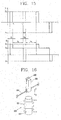
- Figure 14 is a hysterisis curve showing an operating principle of an optical switch drive unit in accordance with an embodiment of the present invention
- Figure 15 is a graph showing variation of magnetic field intensity and magnetic flux density about a pulse input current of the drive unit in accordance with the embodiment of the present invention.
- Graph in Figure 14 shows a correlation between a magnetic filed intensity H and a magnetic flux density B of a magnetic filed formed when current is applied to the coil.
- a magnetic flux density B is varied along a path 11 and a path 13 and finally has a B 0 value.
- a magnetic flux density B is varied along a path 15 and a path 17 and finally has a 0 value. Accordingly, when the magnetic field having a size of H 1 , H 2 is repeatedly applied as a pulse, magnetic flux density as B0 and 0 can be obtained.
- the moving member 200 in order to make the moving member 200 return to the initial state, by applying current to the coil 212 in the opposite direction, the moving member 200 is rotated in the opposite direction and maintains the initial state by the elastic force of the spring 204.
- Figure 16 illustrates a construction of an optical switch drive unit in accordance with another embodiment of the present invention.
- the optical switch drive unit in accordance with another embodiment of the present invention has a construction same with that of the embodiment of the present invention. Only the moving member 206 and the electromagnetic force generator 208 are arranged on the same straight line, when power is applied to the coil 212 of the electromagnetic force generator 208, the moving member 200 performs a linear reciprocating motion up and down as shown as arrows C, D.
- FIGs 17 ⁇ 19 are sectional views illustrating an installation structure of a yoke for providing a line path of magnetic force to an electromagnetic force generator of an optical switch drive unit in accordance with the present invention.
- a yoke 230 is installed at the bottom of the electromagnetic force generator 208.
- a yoke 240 covers the bottom and the side of the electromagnetic force generator 208.
- a yoke 250 is arranged to cover the whole circumference of the electromagnetic force generator 208.
- a line path of magnetic force is provided by the yoke.
Landscapes
- Physics & Mathematics (AREA)
- General Physics & Mathematics (AREA)
- Optics & Photonics (AREA)
- Engineering & Computer Science (AREA)
- Computer Networks & Wireless Communication (AREA)
- Electromagnetism (AREA)
- Mechanical Light Control Or Optical Switches (AREA)
Applications Claiming Priority (5)
| Application Number | Priority Date | Filing Date | Title |
|---|---|---|---|
| KR1020020065335A KR20040036357A (ko) | 2002-10-24 | 2002-10-24 | 저전력 구동이 가능한 광 스위치 |
| KR2002065335 | 2002-10-24 | ||
| KR1020020075488A KR20040047327A (ko) | 2002-11-29 | 2002-11-29 | 광스위치 |
| KR2002075488 | 2002-11-29 | ||
| EP03024431A EP1413913A3 (fr) | 2002-10-24 | 2003-10-23 | Commutateur de brassage optique |
Related Parent Applications (1)
| Application Number | Title | Priority Date | Filing Date |
|---|---|---|---|
| EP03024431A Division EP1413913A3 (fr) | 2002-10-24 | 2003-10-23 | Commutateur de brassage optique |
Publications (2)
| Publication Number | Publication Date |
|---|---|
| EP1577696A2 true EP1577696A2 (fr) | 2005-09-21 |
| EP1577696A3 EP1577696A3 (fr) | 2005-10-19 |
Family
ID=32072574
Family Applications (2)
| Application Number | Title | Priority Date | Filing Date |
|---|---|---|---|
| EP05013442A Withdrawn EP1577696A3 (fr) | 2002-10-24 | 2003-10-23 | Commutateur optique |
| EP03024431A Withdrawn EP1413913A3 (fr) | 2002-10-24 | 2003-10-23 | Commutateur de brassage optique |
Family Applications After (1)
| Application Number | Title | Priority Date | Filing Date |
|---|---|---|---|
| EP03024431A Withdrawn EP1413913A3 (fr) | 2002-10-24 | 2003-10-23 | Commutateur de brassage optique |
Country Status (5)
| Country | Link |
|---|---|
| US (1) | US20040091202A1 (fr) |
| EP (2) | EP1577696A3 (fr) |
| JP (1) | JP2004145348A (fr) |
| CN (1) | CN1499230A (fr) |
| TW (1) | TWI229210B (fr) |
Families Citing this family (9)
| Publication number | Priority date | Publication date | Assignee | Title |
|---|---|---|---|---|
| US6862387B2 (en) * | 2002-06-11 | 2005-03-01 | The United States Of America As Represented By The Secretary Of The Navy | Low-loss compact reflective turns in optical waveguides |
| JP4853962B2 (ja) * | 2006-11-07 | 2012-01-11 | 独立行政法人情報通信研究機構 | 光経路交換装置 |
| EP2394190A4 (fr) | 2009-02-03 | 2018-04-25 | Winchester Electronics Corporation | Prise et connecteur à fibres optiques |
| US9170377B2 (en) | 2011-07-18 | 2015-10-27 | Hewlett-Packard Development Company, L.P. | Optical interconnect |
| US9195008B2 (en) | 2013-02-26 | 2015-11-24 | Winchester Electronics Corporation | Expanded beam optical connector and method of making the same |
| US9366858B2 (en) * | 2014-05-05 | 2016-06-14 | Empire Technology Development Llc | Optically-controlled micromirror device |
| CN105680620A (zh) * | 2015-11-25 | 2016-06-15 | 杨斌堂 | 旋合模式的双稳态动作执行器及电致通透屏和体 |
| CN107346051A (zh) * | 2017-07-19 | 2017-11-14 | 武汉长盈通光电技术有限公司 | 光纤光路耦合微机械系统 |
| CN109283779A (zh) * | 2017-07-20 | 2019-01-29 | 深圳光峰科技股份有限公司 | 用于改变光路的装置及其可调的激光投影装置 |
Family Cites Families (13)
| Publication number | Priority date | Publication date | Assignee | Title |
|---|---|---|---|---|
| JPS59212802A (ja) * | 1983-05-18 | 1984-12-01 | Fujitsu Ltd | 光スイツチ |
| US5945898A (en) * | 1996-05-31 | 1999-08-31 | The Regents Of The University Of California | Magnetic microactuator |
| US6144781A (en) * | 1997-12-31 | 2000-11-07 | At&T Corp. | Symmetrical optical matrix crossconnect apparatus and method therefor |
| US6195478B1 (en) * | 1998-02-04 | 2001-02-27 | Agilent Technologies, Inc. | Planar lightwave circuit-based optical switches using micromirrors in trenches |
| JP4001436B2 (ja) * | 1998-07-23 | 2007-10-31 | 三菱電機株式会社 | 光スイッチ及び光スイッチを用いた光路切換装置 |
| US6962830B1 (en) * | 1999-03-09 | 2005-11-08 | The Regents Of The University Of California | Global mechanical stop |
| JP2001235690A (ja) * | 2000-02-22 | 2001-08-31 | Mitsubishi Electric Corp | 光スイッチ |
| US6490382B1 (en) * | 2000-05-05 | 2002-12-03 | Jds Uniphase Corporation | MicroElectroMechanical optical cross-connect switches having reduced numbers of reflectors therein and methods of operating same |
| DK1352408T3 (da) * | 2001-01-18 | 2007-07-09 | Univ Arizona | Mirko-magnetisk låseomskifter med mindre begrænset udretningsbehov |
| EP1245976A1 (fr) * | 2001-03-30 | 2002-10-02 | Corning O.T.I. S.p.A. | Configuration d'un commutateur optique |
| JP2002323663A (ja) * | 2001-04-25 | 2002-11-08 | Nec Corp | クロスコネクト光スイッチ |
| JP2003035875A (ja) * | 2001-07-24 | 2003-02-07 | Hitachi Ltd | 光スイッチ |
| US6798942B2 (en) * | 2002-04-05 | 2004-09-28 | Finisar Corporation | Zero static power optical switch |
-
2003
- 2003-10-21 TW TW092129128A patent/TWI229210B/zh not_active IP Right Cessation
- 2003-10-21 US US10/688,895 patent/US20040091202A1/en not_active Abandoned
- 2003-10-23 EP EP05013442A patent/EP1577696A3/fr not_active Withdrawn
- 2003-10-23 EP EP03024431A patent/EP1413913A3/fr not_active Withdrawn
- 2003-10-24 JP JP2003364560A patent/JP2004145348A/ja active Pending
- 2003-10-24 CN CNA2003101025972A patent/CN1499230A/zh active Pending
Also Published As
| Publication number | Publication date |
|---|---|
| EP1577696A3 (fr) | 2005-10-19 |
| TW200413762A (en) | 2004-08-01 |
| EP1413913A2 (fr) | 2004-04-28 |
| US20040091202A1 (en) | 2004-05-13 |
| CN1499230A (zh) | 2004-05-26 |
| TWI229210B (en) | 2005-03-11 |
| EP1413913A3 (fr) | 2004-07-21 |
| JP2004145348A (ja) | 2004-05-20 |
Similar Documents
| Publication | Publication Date | Title |
|---|---|---|
| EP1004910B1 (fr) | Système de brassage optique comportant des éléments reconfigurables réfléchissant la lumière | |
| CN107111128B (zh) | 多镜扫描深度引擎 | |
| EP1577696A2 (fr) | Commutateur optique | |
| US7007850B2 (en) | Bar code reading apparatus, moving mirror for bar code reading apparatus, and manufacturing thereof | |
| US6961485B2 (en) | Optical switch | |
| JP4055492B2 (ja) | 光スイッチ | |
| KR100771765B1 (ko) | 광 스위치 | |
| KR20060084307A (ko) | 전자력 구동 스캐닝 마이크로미러 및 이를 사용한광스캐닝 장치 | |
| JP2002323663A (ja) | クロスコネクト光スイッチ | |
| EP1628154A1 (fr) | Commutateur optique | |
| JP3972935B2 (ja) | 光スイッチ及び光スイッチユニット | |
| US20030231820A1 (en) | Optical switch | |
| JP2005215270A (ja) | 光スイッチ | |
| JP3709677B2 (ja) | 光スイッチ | |
| CN118311765A (zh) | Mems振镜芯片、制备方法和光学扫描装置 | |
| KR20040036357A (ko) | 저전력 구동이 가능한 광 스위치 | |
| KR100565598B1 (ko) | 광 스위치 | |
| JP3030553B1 (ja) | 光スイッチ光路切換部の組立方法および光スイッチ | |
| JP2001264652A (ja) | 光スイッチ | |
| JP2007017562A (ja) | 多チャンネル光スイッチ | |
| KR20040025206A (ko) | 정전기식 2축 마이크로 미러 및 그 제조방법 | |
| JPH0458609B2 (fr) | ||
| KR20010109837A (ko) | 광 픽업 엑츄에이터 | |
| JPH03260613A (ja) | 光スイッチ | |
| JP2004240397A (ja) | 光スイッチ |
Legal Events
| Date | Code | Title | Description |
|---|---|---|---|
| PUAI | Public reference made under article 153(3) epc to a published international application that has entered the european phase |
Free format text: ORIGINAL CODE: 0009012 |
|
| PUAL | Search report despatched |
Free format text: ORIGINAL CODE: 0009013 |
|
| 17P | Request for examination filed |
Effective date: 20050622 |
|
| AC | Divisional application: reference to earlier application |
Ref document number: 1413913 Country of ref document: EP Kind code of ref document: P |
|
| AK | Designated contracting states |
Kind code of ref document: A2 Designated state(s): AT BE BG CH CY CZ DE DK EE ES FI FR GB GR HU IE IT LI LU MC NL PT RO SE SI SK TR |
|
| AK | Designated contracting states |
Kind code of ref document: A3 Designated state(s): AT BE BG CH CY CZ DE DK EE ES FI FR GB GR HU IE IT LI LU MC NL PT RO SE SI SK TR |
|
| RIN1 | Information on inventor provided before grant (corrected) |
Inventor name: JI, CHANG HYEON Inventor name: YEE, YOUNG JOOMAEWHA MAEUL JUGONG APT. 210-604 Inventor name: BU, JONG UK |
|
| RIN1 | Information on inventor provided before grant (corrected) |
Inventor name: BU, JONG UK Inventor name: JI, CHANG HYEON Inventor name: YEE, YOUNG JOOTAPMAEUL GYEONGNAM APT. 707-304 |
|
| AKX | Designation fees paid |
Designated state(s): AT BE BG CH CY CZ DE DK EE ES FI FR GB GR HU IE IT LI LU MC NL PT RO SE SI SK TR |
|
| 17Q | First examination report despatched |
Effective date: 20060823 |
|
| STAA | Information on the status of an ep patent application or granted ep patent |
Free format text: STATUS: THE APPLICATION IS DEEMED TO BE WITHDRAWN |
|
| 18D | Application deemed to be withdrawn |
Effective date: 20070103 |