EP1574475A2 - Integrierte Ansteuerelektronik für ein MEMS Bauelement mit Hochspannungs-Dünnfilmtransistoren - Google Patents
Integrierte Ansteuerelektronik für ein MEMS Bauelement mit Hochspannungs-Dünnfilmtransistoren Download PDFInfo
- Publication number
- EP1574475A2 EP1574475A2 EP05251214A EP05251214A EP1574475A2 EP 1574475 A2 EP1574475 A2 EP 1574475A2 EP 05251214 A EP05251214 A EP 05251214A EP 05251214 A EP05251214 A EP 05251214A EP 1574475 A2 EP1574475 A2 EP 1574475A2
- Authority
- EP
- European Patent Office
- Prior art keywords
- electrode
- hvtft
- actuating
- source
- voltage
- Prior art date
- Legal status (The legal status is an assumption and is not a legal conclusion. Google has not performed a legal analysis and makes no representation as to the accuracy of the status listed.)
- Granted
Links
- 239000010409 thin film Substances 0.000 title claims abstract description 8
- 239000000758 substrate Substances 0.000 claims abstract description 50
- 239000000463 material Substances 0.000 claims description 16
- 239000003990 capacitor Substances 0.000 claims description 10
- 230000005686 electrostatic field Effects 0.000 claims description 9
- 239000004065 semiconductor Substances 0.000 claims description 9
- 239000011521 glass Substances 0.000 claims description 8
- 239000000919 ceramic Substances 0.000 claims description 5
- 239000004033 plastic Substances 0.000 claims description 4
- 229920003023 plastic Polymers 0.000 claims description 4
- 239000010935 stainless steel Substances 0.000 claims description 4
- 229910001220 stainless steel Inorganic materials 0.000 claims description 4
- 238000003491 array Methods 0.000 abstract description 8
- 230000015556 catabolic process Effects 0.000 abstract description 7
- 230000005540 biological transmission Effects 0.000 abstract description 2
- 230000015572 biosynthetic process Effects 0.000 abstract description 2
- 239000010410 layer Substances 0.000 description 26
- 238000000034 method Methods 0.000 description 21
- 229910052751 metal Inorganic materials 0.000 description 10
- 239000002184 metal Substances 0.000 description 10
- 150000004767 nitrides Chemical class 0.000 description 8
- 238000004519 manufacturing process Methods 0.000 description 7
- PXHVJJICTQNCMI-UHFFFAOYSA-N Nickel Chemical compound [Ni] PXHVJJICTQNCMI-UHFFFAOYSA-N 0.000 description 6
- 229910021417 amorphous silicon Inorganic materials 0.000 description 6
- 239000003989 dielectric material Substances 0.000 description 5
- XUIMIQQOPSSXEZ-UHFFFAOYSA-N Silicon Chemical compound [Si] XUIMIQQOPSSXEZ-UHFFFAOYSA-N 0.000 description 4
- 238000010586 diagram Methods 0.000 description 4
- 238000005516 engineering process Methods 0.000 description 4
- 229910052710 silicon Inorganic materials 0.000 description 4
- 239000010703 silicon Substances 0.000 description 4
- 239000010936 titanium Substances 0.000 description 4
- 101100406515 Drosophila melanogaster orb2 gene Proteins 0.000 description 3
- 101100258025 Schizosaccharomyces pombe (strain 972 / ATCC 24843) shk1 gene Proteins 0.000 description 3
- 238000005452 bending Methods 0.000 description 3
- 239000011229 interlayer Substances 0.000 description 3
- 229910052581 Si3N4 Inorganic materials 0.000 description 2
- RTAQQCXQSZGOHL-UHFFFAOYSA-N Titanium Chemical compound [Ti] RTAQQCXQSZGOHL-UHFFFAOYSA-N 0.000 description 2
- 239000011651 chromium Substances 0.000 description 2
- 239000004020 conductor Substances 0.000 description 2
- 239000010949 copper Substances 0.000 description 2
- 238000000151 deposition Methods 0.000 description 2
- 239000010408 film Substances 0.000 description 2
- 230000010354 integration Effects 0.000 description 2
- 238000002955 isolation Methods 0.000 description 2
- 239000011159 matrix material Substances 0.000 description 2
- 150000002739 metals Chemical class 0.000 description 2
- 229910052759 nickel Inorganic materials 0.000 description 2
- 239000000523 sample Substances 0.000 description 2
- HQVNEWCFYHHQES-UHFFFAOYSA-N silicon nitride Chemical compound N12[Si]34N5[Si]62N3[Si]51N64 HQVNEWCFYHHQES-UHFFFAOYSA-N 0.000 description 2
- 229910052719 titanium Inorganic materials 0.000 description 2
- JBRZTFJDHDCESZ-UHFFFAOYSA-N AsGa Chemical compound [As]#[Ga] JBRZTFJDHDCESZ-UHFFFAOYSA-N 0.000 description 1
- VYZAMTAEIAYCRO-UHFFFAOYSA-N Chromium Chemical compound [Cr] VYZAMTAEIAYCRO-UHFFFAOYSA-N 0.000 description 1
- RYGMFSIKBFXOCR-UHFFFAOYSA-N Copper Chemical compound [Cu] RYGMFSIKBFXOCR-UHFFFAOYSA-N 0.000 description 1
- 229910001218 Gallium arsenide Inorganic materials 0.000 description 1
- ZOKXTWBITQBERF-UHFFFAOYSA-N Molybdenum Chemical compound [Mo] ZOKXTWBITQBERF-UHFFFAOYSA-N 0.000 description 1
- 239000004642 Polyimide Substances 0.000 description 1
- 229910001080 W alloy Inorganic materials 0.000 description 1
- 229910045601 alloy Inorganic materials 0.000 description 1
- 239000000956 alloy Substances 0.000 description 1
- 229910052782 aluminium Inorganic materials 0.000 description 1
- XAGFODPZIPBFFR-UHFFFAOYSA-N aluminium Chemical compound [Al] XAGFODPZIPBFFR-UHFFFAOYSA-N 0.000 description 1
- 230000009286 beneficial effect Effects 0.000 description 1
- 238000006243 chemical reaction Methods 0.000 description 1
- 229910052804 chromium Inorganic materials 0.000 description 1
- 239000011248 coating agent Substances 0.000 description 1
- 238000000576 coating method Methods 0.000 description 1
- 239000010941 cobalt Substances 0.000 description 1
- 229910017052 cobalt Inorganic materials 0.000 description 1
- GUTLYIVDDKVIGB-UHFFFAOYSA-N cobalt atom Chemical compound [Co] GUTLYIVDDKVIGB-UHFFFAOYSA-N 0.000 description 1
- 229910052802 copper Inorganic materials 0.000 description 1
- 230000008878 coupling Effects 0.000 description 1
- 238000010168 coupling process Methods 0.000 description 1
- 238000005859 coupling reaction Methods 0.000 description 1
- 238000005137 deposition process Methods 0.000 description 1
- 238000011161 development Methods 0.000 description 1
- 230000018109 developmental process Effects 0.000 description 1
- 229920002457 flexible plastic Polymers 0.000 description 1
- 238000005286 illumination Methods 0.000 description 1
- 239000011810 insulating material Substances 0.000 description 1
- 239000012212 insulator Substances 0.000 description 1
- 239000004973 liquid crystal related substance Substances 0.000 description 1
- 238000005459 micromachining Methods 0.000 description 1
- 229910052750 molybdenum Inorganic materials 0.000 description 1
- 239000011733 molybdenum Substances 0.000 description 1
- 230000003287 optical effect Effects 0.000 description 1
- 239000011368 organic material Substances 0.000 description 1
- 238000000059 patterning Methods 0.000 description 1
- 230000002093 peripheral effect Effects 0.000 description 1
- 229910021420 polycrystalline silicon Inorganic materials 0.000 description 1
- 229920001721 polyimide Polymers 0.000 description 1
- 229920000642 polymer Polymers 0.000 description 1
- VSZWPYCFIRKVQL-UHFFFAOYSA-N selanylidenegallium;selenium Chemical compound [Se].[Se]=[Ga].[Se]=[Ga] VSZWPYCFIRKVQL-UHFFFAOYSA-N 0.000 description 1
- MAKDTFFYCIMFQP-UHFFFAOYSA-N titanium tungsten Chemical compound [Ti].[W] MAKDTFFYCIMFQP-UHFFFAOYSA-N 0.000 description 1
- WFKWXMTUELFFGS-UHFFFAOYSA-N tungsten Chemical compound [W] WFKWXMTUELFFGS-UHFFFAOYSA-N 0.000 description 1
- 229910052721 tungsten Inorganic materials 0.000 description 1
- 239000010937 tungsten Substances 0.000 description 1
Images


Classifications
-
- H—ELECTRICITY
- H10—SEMICONDUCTOR DEVICES; ELECTRIC SOLID-STATE DEVICES NOT OTHERWISE PROVIDED FOR
- H10D—INORGANIC ELECTRIC SEMICONDUCTOR DEVICES
- H10D86/00—Integrated devices formed in or on insulating or conducting substrates, e.g. formed in silicon-on-insulator [SOI] substrates or on stainless steel or glass substrates
- H10D86/201—Integrated devices formed in or on insulating or conducting substrates, e.g. formed in silicon-on-insulator [SOI] substrates or on stainless steel or glass substrates the substrates comprising an insulating layer on a semiconductor body, e.g. SOI
-
- B—PERFORMING OPERATIONS; TRANSPORTING
- B81—MICROSTRUCTURAL TECHNOLOGY
- B81C—PROCESSES OR APPARATUS SPECIALLY ADAPTED FOR THE MANUFACTURE OR TREATMENT OF MICROSTRUCTURAL DEVICES OR SYSTEMS
- B81C1/00—Manufacture or treatment of devices or systems in or on a substrate
- B81C1/00015—Manufacture or treatment of devices or systems in or on a substrate for manufacturing microsystems
- B81C1/00222—Integrating an electronic processing unit with a micromechanical structure
- B81C1/00246—Monolithic integration, i.e. micromechanical structure and electronic processing unit are integrated on the same substrate
-
- H—ELECTRICITY
- H10—SEMICONDUCTOR DEVICES; ELECTRIC SOLID-STATE DEVICES NOT OTHERWISE PROVIDED FOR
- H10D—INORGANIC ELECTRIC SEMICONDUCTOR DEVICES
- H10D30/00—Field-effect transistors [FET]
- H10D30/60—Insulated-gate field-effect transistors [IGFET]
- H10D30/67—Thin-film transistors [TFT]
- H10D30/6704—Thin-film transistors [TFT] having supplementary regions or layers in the thin films or in the insulated bulk substrates for controlling properties of the device
- H10D30/6713—Thin-film transistors [TFT] having supplementary regions or layers in the thin films or in the insulated bulk substrates for controlling properties of the device characterised by the properties of the source or drain regions, e.g. compositions or sectional shapes
- H10D30/6715—Thin-film transistors [TFT] having supplementary regions or layers in the thin films or in the insulated bulk substrates for controlling properties of the device characterised by the properties of the source or drain regions, e.g. compositions or sectional shapes characterised by the doping profiles, e.g. having lightly-doped source or drain extensions
- H10D30/6717—Thin-film transistors [TFT] having supplementary regions or layers in the thin films or in the insulated bulk substrates for controlling properties of the device characterised by the properties of the source or drain regions, e.g. compositions or sectional shapes characterised by the doping profiles, e.g. having lightly-doped source or drain extensions the source and the drain regions being asymmetrical
-
- B—PERFORMING OPERATIONS; TRANSPORTING
- B81—MICROSTRUCTURAL TECHNOLOGY
- B81B—MICROSTRUCTURAL DEVICES OR SYSTEMS, e.g. MICROMECHANICAL DEVICES
- B81B2203/00—Basic microelectromechanical structures
- B81B2203/01—Suspended structures, i.e. structures allowing a movement
- B81B2203/0118—Cantilevers
-
- B—PERFORMING OPERATIONS; TRANSPORTING
- B81—MICROSTRUCTURAL TECHNOLOGY
- B81C—PROCESSES OR APPARATUS SPECIALLY ADAPTED FOR THE MANUFACTURE OR TREATMENT OF MICROSTRUCTURAL DEVICES OR SYSTEMS
- B81C2203/00—Forming microstructural systems
- B81C2203/07—Integrating an electronic processing unit with a micromechanical structure
- B81C2203/0707—Monolithic integration, i.e. the electronic processing unit is formed on or in the same substrate as the micromechanical structure
- B81C2203/0735—Post-CMOS, i.e. forming the micromechanical structure after the CMOS circuit
Definitions
- This invention relates to microelectro-mechanical (MEMS) devices, and more particularly to actuated MEMS devices and driver circuits for controlling actuated MEMS devices.
- MEMS microelectro-mechanical
- Photolithographically patterned micro spring structures represent one form of MEMS devices that have been developed.
- a typical micro spring structure includes a spring finger having an anchor portion secured to a substrate or other supporting structure, and a free (cantilevered) portion extending from the anchored portion over the substrate.
- Recent developments related to micro spring-type MEMS devices include the ability to actuate (i.e., control the position of) a tip portion of a released spring finger by selectively applying an electrostatic actuating force to pull the cantilevered free portion toward the underlying substrate (i.e., against the bending force generated by the internal stress gradient of the spring finger).
- a problem associated with electrostatically actuated MEMS devices is that, although the actuating stroke length is generally proportional to the applied voltage, the maximum force is usually proportional to the voltage squared. Therefore, in practical applications, a high voltage (i.e., in excess of 50 Volts, often 100 V or more) is needed to drive these electrostatically actuated MEMS devices. Supplying this high voltage to the electrode of an electrostatically actuated MEMS device is not a major concern because many efficient DC-DC conversion power supplies are readily available, especially for the low current requirement of most electrostatically actuated MEMS devices. Controlling the high voltage, however, is not straight forward because such high voltages are not compatible with standard CMOS ULSI technology.
- CMOS ULSI technology produces circuit structures having operating voltages in the range of about 0 V to 20 V.
- special high voltage power chips are currently used to interface between the control circuitry and the actuated MEMS devices.
- external power chips can be purchased "off the shelf” (i.e., relatively inexpensively)
- the use of external power chips requires a separate connection for each MEMS device. Accordingly, it would be very difficult and expensive to produce large MEMS device arrays using external power chips because the number of required interconnects increases as the square of array size, which increases both manufacturing time and cost.
- each offset-gate HVTFT includes a controlling gate electrode, source electrode positioned relatively close to the gate electrode, and a drain electrode arranged in an offset position that is relatively far from the gate electrode, and such that a lateral offset region is defined between the drain electrode and the gate electrode.
- offset-gate HVTFTs can be made using typical TFT fabrication processes (which are generally compatible with the fabrication of MEMS devices), but provide unique input/output properties that facilitate control of the high actuating voltages using "normal" operating (i.e., gate) voltages. That is, the drain current of the offset-gate HVTFTs can be changed by eight orders of magnitude by changing the gate voltage between "normal" low and high operating voltage levels (e.g., -5V to 20V).
- This feature offers the possibility of designing driver circuits using conventional (i.e., symmetric) TFT control circuits that are subjected to "normal" operating voltage swings, and using offset-gate HVTFTs only in the last stage (i.e., to couple and decouple the MEMS device to/from the high actuating voltage).
- the driver electronics for the integrated MEMS/HVTFT apparatus are arranged such that the drain electrode of selected HVTFTs are coupled to both an associated MEMS device and the high actuating voltage (i.e., a voltage source with a finite internal impedance), and the source electrode of the selected HVTFT is coupled to a low voltage source (e.g., ground).
- the high actuating voltage i.e., a voltage source with a finite internal impedance
- a low voltage source e.g., ground
- the actuating voltage applied to the MEMS device is inversely proportional to the control signal transmitted on the gate electrode.
- a minimum (low) control signal voltage e.g., zero volts
- an intermediate control signal voltage e.g., 5 V
- an intermediate control signal voltage is transmitted on the gate electrode of the HVTFT, thereby partially turning on the HVTFT and reducing the actuating voltage on the drain electrode to an intermediate level.
- a maximum (high) control signal voltage (e.g., 20 V) is applied to the gate electrode of the HVTFT, thereby fully turning on the HVTFT and grounding the drain electrode (i.e., essentially eliminating the actuating voltage passed to the MEMS device).
- an active load driver circuit includes two offset-gate HVTFTs connected in series between the high voltage source and ground, with the first HVTFT having gate and source electrodes connected to the high voltage source, the second HVTFT having a source electrode connected to ground and a gate electrode connected to receive the "normal" voltage control signal.
- the actuating electrode of an associated MEMS device is controlled by an intermediate node connected to the drain electrodes of the two HVTFTs.
- the first HVTFT serves as a resistor between the high voltage source and the intermediate node, thereby eliminating the need for a costly and space inefficient resistor structure.
- a driver circuit includes an alternating-current (AC) voltage supply that transmits a high voltage AC signal onto the actuating electrode (or anchor portion of a MEMS structure) of an associated MEMS device, and an associated HVTFT has a drain electrode connected to the anchor portion of the MEMS structure(or actuating voltage), a source electrode coupled to a low voltage source (e.g., via a capacitor), and a gate electrode connected to receive a "normal" control signal from the control circuit. Similar to the first specific embodiment, the HVTFT is arranged to prevent high voltages across the source/gate dielectric, thereby minimizing dielectric breakdown.
- AC alternating-current
- Fig. 1 is a perspective view showing a simplified apparatus 100 according to an exemplary embodiment of the present invention.
- Apparatus 100 includes an actuated MEMS device 110 and an actuating (driver) circuit 130 that are integrally fabricated on a substrate 101.
- actuating (driver) circuit 130 includes an offset-gate HVTFT 140 that is utilized to selectively transmit a relatively high actuating voltage (i.e., 50 V or greater) in response to a relatively low control voltage (i.e., 10 V or less) that is provided from an associated control logic circuit 150.
- a relatively high actuating voltage i.e., 50 V or greater
- a relatively low control voltage i.e. 10 V or less
- substrate 101 is formed using an insulating material such as glass, ceramic, plastic, and a flexible substrate, and in one embodiment includes at least one dielectric layer 105 and a semiconductor layer 107 formed thereon.
- a semiconductor region 107 is formed using any of amorphous silicon (a-Si:H), polycrystalline silicon, and organic material.
- substrate 101 may be formed using conductive materials, such as stainless steel, and may also comprise a semiconductor material such as silicon or gallium arsenide (with or without an active integrated circuit including, for example, control logic circuit 150).
- actuated MEMS device refers to an integration of a micromechanical MEMS structure and an actuating electrode that are combined on a common substrate through microfabrication technology.
- the actuating electrodes (and associated control circuitry) are fabricated using selected integrated circuit (IC) process sequences, and the MEMS structures are fabricated using "micromachining" processes that are compatible with the selected IC process sequences. Referring to the left side of Fig.
- actuated MEMS device 110 includes a fixed actuating electrode 115 formed over the substrate (i.e., on dielectric layer 105), and a micro spring (MEMS) structure (i.e., a movable counterpart) 120 including an anchor portion 122 that is fixedly (rigidly) attached to substrate 101, and a cantilevered movable (free) portion 125 that extends from anchor portion 122 over actuating electrode 115.
- MEMS micro spring
- micro spring structure 120 is produced such that it includes an internal stress (or strain) gradient that biases free portions 125 away from substrate 101, thereby producing the indicated curved shape that points tip 127 in a direction away from actuating electrode 115.
- the movable counterpart of an actuated MEMS device may include, for example, a metal beam or diaphragm that is electrostatically actuated in response to an actuating voltage applied to one of the movable counterpart or the fixed electrode (with the other structure grounded or coupled to a suitable signal).
- the movable counterpart of an actuated MEMS device may be actuated by two fixed electrodes that are capacitively coupled to the movable counterpart, with one of the fixed electrodes held at ground and the other fixed electrode selectively receiving a control (high) voltage.
- Each HVTFT is a Thin Film Transistor (TFT) in which the shortest distance between any part of the drain electrode and controlling gate electrode is significantly larger than the thickness of gate dielectric (i.e., the distance between the gate electrode and the source electrode), such that the break down voltage between drain and source is larger than the break down voltage between gate and source.
- TFT Thin Film Transistor
- each HVTFT 140 generally includes a controlling gate electrode 142 formed on substrate 101 below dielectric layer 105, a source electrode 144 and a drain electrode 146 formed on the dielectric layer 105 and on opposite ends of semiconductor region 107.
- each HVTFT 140 is distinguished over standard TFTs in that gate electrode 142 is offset (i.e., such that a portion of source electrode 144 is substantially located over or laterally overlaps gate 142, e.g., by a distance D1, but in contrast drain electrode 146 is laterally offset from gate structure 142 by a distance D2).
- this offset-gate arrangement differs from the source/drain symmetry associated with standard TFTs, and facilitates the controlled passage of high voltages (e.g., 50 to 400 V or higher, depending on the selected scaling) using a relatively low control voltage (e.g., 0 to 20 V) generated by control logic circuit 150,which in one embodiment is fabricated using conventional CMOS techniques or TFT circuits.
- control logic circuit 150 which in one embodiment is fabricated using conventional CMOS techniques or TFT circuits.
- HVTFT 140 is arranged such that drain terminal 146 is coupled to the high actuating voltage (ACTUATING VOLTAGE SOURCE, which in one embodiment is a voltage source with a finite internal impedance) used to actuate MEMS device 110, and source terminal 144 is connected to a low voltage source (e.g., ground).
- ACTUATING VOLTAGE SOURCE which in one embodiment is a voltage source with a finite internal impedance
- the actuating voltage applied to MEMS device 110 is inversely proportional to the control signal transmitted on gate electrode 142. Accordingly, the present invention facilitates the control of the high actuating voltages applied to MEMS device 110 using relatively low control voltages transmitted on gate electrode 142, while minimizing the chance of dielectric breakdown caused by the transmitted high actuating voltages.
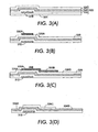
- Figs. 2(A) through 2(C) depict MEMS device 110 during various states of actuation.
- Fig. 2(A) depicts MEMS device 110 in a fully retracted position in which tip 127 contacts actuating electrode 115 and/or other structures formed on substrate 101 (e.g., an electrically insulating film formed on electrode 115).
- This fully retracted position is achieved when a gate voltage transmitted on gate electrode 142 by control logic circuit 150 (Fig. 1) is minimized (e.g., zero volts), thereby turning off HVTFT 140 and preventing the high voltage present on drain electrode 146 (and actuating electrode 115) from passing to source electrode 144.
- a relatively strong (first) electrostatic field EF1 is generated that causes movable portion 125 to move into the fully retracted position shown in Fig. 2(A).
- Fig. 2(B) depicts MEMS device 110 in a partially retracted position in which tip 127 of micro spring structure 120 is between the fully retracted position shown in Fig. 2(A) and the fully deployed position described below.
- This partially retracted position is achieved when MEMS device 110 is in a partially turned on state, that is, when a gate voltage V1 transmitted on gate electrode 142 by control logic circuit 150 (Fig. 1) is at a selected intermediate level (e.g., 5 V) that partially turns on HVTFT 140.
- a control current CC1 is generated from drain electrode 146 to source electrode 144 that reduces the voltage on actuating electrode 115, which in turn weakens the attractive electrostatic force transmitted from actuating electrode 115 on movable portion 125 of micro spring structure 120.
- movable portion 125 bends away from substrate 101, due to its internal stress gradient, until the bending force BF1 generated by the internal stress gradient balances with the relatively weak (second) electrostatic field EF2 movable portion 125, thereby moving into the partially retracted position relative to substrate 101 that is shown in Fig. 2(B).
- Fig. 2(C) depicts MEMS device 110 in a fully deployed position in which tip 127 of micro spring structure 120 is at a maximum distance from actuating electrode 115.
- This fully deployed position is achieved when MEMS device 110 is in a fully turned on state, that is, when a gate voltage V2 transmitted on gate electrode 142 is at a maximum level (e.g., 10 V) that fully turns on HVTFT 140, thereby draining the maximum control current CC2 (e.g., 100 V) from actuating electrode 115 (via channel 105A and source electrode 144 to ground).
- V2 maximum level
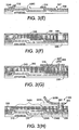
- Figs. 3(A) through 3(H) depict a process for fabricating an integrated MEMS/HVTFT apparatus according to another embodiment of the present invention.
- Fig. 3(A) depicts the formation of a gate electrode 310 on a substrate 301 (which is omitted from 3(B) through 3(H) for brevity) according to known techniques.
- a-Si:H layer 320 including a lower nitride layer 322, an intermediate silicon (undoped) layer 324 (which forms the semiconductor region of the subsequently formed TFT structures), and an upper nitride layer 326.
- a first resist portion 330A is formed on a first section 326A of upper nitride layer 326 over gate electrode 310, e.g., using know backside illumination techniques.
- a second resist portion 330B is then formed using known techniques such that second resist portion 330B extends from first section 326A over a second section 326B of upper nitride layer 326.
- a metal layer, or a doped a-Si:H and metal multi-layer is then deposited and patterned to form a source electrode 332 that extends partially over a first edge of upper nitride portion 326C, a drain/actuating electrode 334 that extends partially over a second edge of upper nitride portion 326C, and an electrode 336 that is separated from drain/actuating electrode 334 by a gap 337.
- an interlayer (second) dielectric layer 340 e.g., _Silicon Oxynitride, BCB, or polyimide
- a release (sacrificial) material layer 350 are then formed over the existing structure, and patterned using known techniques to form an opening 345 that exposes a portion of electrode 336.
- release material layer 350 is Titanium (Ti) that is deposited (e.g., sputtered) to a thickness of approximately 0.05 microns or greater.
- release materials having the beneficial characteristics of titanium may also be used, and may include at least one of Copper (Cu), Aluminum (Al), Nickel (Ni), Zirconium (Zr), Cobalt (Co), or a non-conducting material such as silicon (Si) or Silicon Nitride (SiN).
- two or more release material layers can be sequentially deposited to form a multi-layer structure.
- any of the above-mentioned release materials can be sandwiched between two non-release material layers (i.e., materials that are not removed during the spring release process, described below).
- a stress-engineered spring structure 360 is formed by depositing and patterning a spring material layer on release layer 350 such that an anchor portion 362 extends into opening 345 and contacts electrode 336, and a movable portion 365 extends over at least a portion of drain/actuating electrode 334 (i.e., either directly over the actuating electrode, or laterally offset from, for example, a tapered actuating electrode such those as disclosed in U.S. Patent No. 6,734,425 (issued from application serial number 10/136,258, entitled "SCANNING PROBE SYSTEM WITH SPRING PROBE AND ACTUATION/SENSING STRUCTURE", which is incorporated by reference in its entirety.
- the spring material forming spring structure 360 is a stress-engineered metal film formed such that it includes internal stress variations in the growth direction (that is, the internal stress varies in proportion to its vertical thickness or distance from the release layer 350.
- Methods for generating internal stress variations in spring structure 360 are taught, for example, in U.S. Patent No. 3,842,189 (depositing two metals having different internal stresses) and U.S. Patent No. 5,613,861 (e.g., single metal sputtered while varying process parameters), both of which being incorporated herein by reference.
- spring structure 360 includes one or more metals suitable for forming a micro spring finger (e.g., one or more of molybdenum (Mo), a "moly-chrome” alloy (MoCr), tungsten (W), a titanium-tungsten alloy (Ti:W), chromium (Cr), and nickel (Ni)).
- Mo molybdenum
- MoCr molybdenum
- W tungsten
- Ti:W titanium-tungsten alloy
- Cr chromium
- Ni nickel
- spring structure 360 can be formed using known TFT compatible MEMS deposition processes, including a low stress metal MEMS process, polymer MEMS process, or low temperature bonding to traditional Si MEMS process.
- release material layer 350 is removed (etched) to release movable portion 365 of spring structure 360. As indicated in Fig. 3(H), the removal of the release material layer causes the released movable portion to move from fully retracted position 365A to fully deployed position 365B due to the internal stress gradient.
- HVTFT 140A defines an offset region OR between a right edge of gate electrode 310 and drain electrode 334A.
- interlayer dielectric layer 340 is positioned between actuating electrode 334B and movable portion 365B of spring structure 360.
- the present invention is also directed to specific driver circuits, which are described in the following exemplary embodiments.
- conventional high voltage driver circuits typically utilize high value resistors (in Giga-Ohm range).
- resistors in Giga-Ohm range.
- a problem with using such resistor-based driver circuits is that these resistors are difficult to integrate on-chip, as they require significant chip space and require extra mask steps.
- Another draw back of using resistors are the difficulty of controlling the exact resistance value. These resistors also result in steep transfer curves that give poor analog actuation control, and are better suited for binary applications.
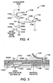
- Fig. 4 is a simplified diagram showing an apparatus 100B including "all-transistor" high voltage driver circuit 130B for controlling an electrostatically actuated MEMS device 110B according to another embodiment of the present invention.
- Driver circuit 130B utilizes two offset-gate HVTFTs 140B1 and 140B2 connected in series between a high voltage source and ground, with an intermediate node N1 being connected to actuating electrode 115B of actuated MEMS device 110B.
- First (load) HVTFT 140B1 has a source electrode 144B1 connected to the high voltage source, a drain electrode 146B1 connected to intermediate node N1, and gate electrode 142B1 also connected to the high voltage source and offset such that an offset region ORB1 is located between gate electrode 142B1 and drain electrode 146B1 (i.e., away from the high voltage source). Note that source electrode 144B1 and gate electrode 142B1 are both connected to the high (actuating) voltage source.
- second (control) HVTFT 140B2 has a source electrode 144B2 connected to ground, a drain electrode 146B2 connected to intermediate node N1, and gate electrode 142B2 arranged such that offset region ORB2 is located between gate electrode 142B2 and drain electrode 146B2 (i.e., away from ground).
- An input voltage e.g., received from control logic circuit 150; see Fig. 1
- gate terminal 142B2 controls the actuating voltage AVB at intermediate node N1 (and, thus, on actuating electrode 115B) by controlling the conductance of second HVTFT 140B2.
- actuated MEMS device 110B includes a MEMS structure 120B having an anchor portion 122B connected to a low voltage source (e.g., ground), and a movable portion 125B positioned over actuating electrode 115B.
- a low voltage source e.g., ground
- a movable portion 125B positioned over actuating electrode 115B.
- the electrostatic force applied on MEMS structure 120B from actuating electrode 115B overcomes the bending force generated by the internal stress gradient, thereby causing movable portion 125B to bend toward actuating electrode 115B in the manner described above. Accordingly, the "all-transistor" high voltage driver circuit 130B shown in Fig. 4 facilitates actuation of MEMS device 110B while avoiding the problems associated with resistor-based driver circuits, described above.
- fabricating apparatus 100B using the process flow described with reference to Figs. 3(A) through 3(H) not only provides three-dimensional (3D) integration of MEMS device 110B and driver circuit 130B (Fig. 4), but also enables superior voltage isolation.
- the high voltage applied to actuating electrode 115B from node N1 is applied to drain electrode 146B2, which is separated from gate electrode 142B2 by lateral offset region ORB2, thereby applying drain/gate region VGD over a relatively wide section of dielectric material.
- drain electrode 146B2 which is separated from gate electrode 142B2 by lateral offset region ORB2
- source/gate voltage VSG which is maintained at "normal” (i.e., relatively low) operating voltages, is applied across a relatively narrow section of dielectric material separating source electrode 144B2 and gate electrode 142B2. Accordingly, by providing a suitably wide offset region ORB2, driver circuit 130B (Fig. 4) is constructed such that the probability of dielectric breakdown due to the high actuating voltage applied across HVTFT 140B2 is minimized. Further, although not shown, thick interlayer dielectric insulator and air bridge crossover structures are provided at all high voltage cross-over points (i.e., where metal lines connected to the high actuating voltage source cross metal lines connected to the control logic circuit or ground), thereby minimizing crossover dielectric breakdown.
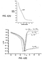
- Fig. 6(A) depicts a graph showing an experimentally generated typical actuating voltage AVB which was generated by the circuit shown in Fig. 4 (i.e., using a-Si:H HVTFTs), which suggests important information for building transistor only NMOS circuits.
- Fig. 6(B) in the reverse bias region (i.e., -100V ⁇ VDS ⁇ 0V), substantial, controllable current flows through the HVTFTs, while VGS is limited to 20V. All transistor HVTFT inverters operating at 100V has been demonstrated with input voltage from 0 to 10V, which can be generated using standard digital-to-analog (D/A) circuits.
- D/A digital-to-analog
- Fig. 7 is a simplified circuit diagram showing an apparatus 100C including a driver circuit 130C that drives an actuated MEMS device 110C using an AC high voltage supply 610 and an associated offset-gate HVTFT 140C according to another specific embodiment of the present invention.
- AC high voltage supply 610 transmits a high voltage AC signal DV to actuating electrode 115C of actuated MEMS device 110C.
- Actuated MEMS device 110C also includes a MEMS structure 120C having an anchor portion 122C and a movable portion 125C positioned over actuating electrode 115C.
- Anchor portion 122C is connected to a drain electrode 146C of offset-gate HVTFT 140C, which also includes a source electrode 144C coupled to ground via a source (first) capacitor C1, and a gate electrode connected to a node N2, which receives a control (data) signal via a "normal" (i.e., symmetrical) TFT 620 and is also coupled to ground via a second capacitor C2.
- associated HVTFT 140C is controlled (turned on and off) by the data signal transmitted on a data line DL, which is selectively passed by TFT 620 in response to a gate signal transmitted on gate line GL. As indicated in Fig.
- the amplitude of the control signal transmitted on data line DL is substantially lower than that of the high voltage AC signal DV.
- the purpose of this control circuit is for quasi-static actuating the MEMS device, and the control signal should be a low voltage, near DC signal relative to the high voltage AC source.
- actuating electrode 115C is charged until the voltage of source capacitor C1 is higher than the control voltage received from data line DL minus the threshold voltage of HVTFT 140C.
- driver circuit 130C avoids cross-over dielectric breakdown by limiting the high voltage to electrode 115C (i.e., from its coupling with movable portion 122C) and drain electrode 146C, which is separated from gate electrode 142C by lateral offset region ORC, thereby applying drain/gate region VGD over a relatively wide section of dielectric material.
- a main advantage provided by the present invention is that apparatus integrating both electrostatically actuated MEMS devices and HVTFT-based driver circuits in the manner described above are able to support large-scale MEMS arrays using a minimum number of surface contacts.
- Large-scale MEMS arrays i.e., including multiple rows and columns of actuated MEMS devices
- the HVTFT-based driver circuits described herein provide a solution for building this type of large-scale MEMS array actuating system.
- Active Matrix switching networks similar to those used to drive Active Matrix Liquid Crystal Displays are a natural solution for driving arrays of MEMS devices with only reasonable amount of peripheral circuits.
- the present invention provides HVTFT-based driver circuits that facilitate integrated driver control on electrostatically actuated MEMS device arrays.
- TFT electronics have the advantage of versatility of choosing substrate, large area, and low cost per unit area.
- Versatility of choosing substrate is a major advantage: 1) standard glass substrate provides superior isolation such that high voltage is easy to handle, 2) glass or other transparent substrates provide wide freedom of designing optical system, 3) glass, ceramic, or other insulative substrates provide low loss to high frequency EM signal and are particular useful for high frequency application, 4) glass is a standard bio-compatible substrate, 5) flexible plastic substrate allow for novel curved substrate applications and 6) even conventional active ICs to form a completely integrated system.
Landscapes
- Engineering & Computer Science (AREA)
- Manufacturing & Machinery (AREA)
- Microelectronics & Electronic Packaging (AREA)
- Micromachines (AREA)
- Thin Film Transistor (AREA)
- Physical Or Chemical Processes And Apparatus (AREA)
- Electroluminescent Light Sources (AREA)
Applications Claiming Priority (2)
| Application Number | Priority Date | Filing Date | Title |
|---|---|---|---|
| US799237 | 2004-03-11 | ||
| US10/799,237 US6912082B1 (en) | 2004-03-11 | 2004-03-11 | Integrated driver electronics for MEMS device using high voltage thin film transistors |
Publications (3)
| Publication Number | Publication Date |
|---|---|
| EP1574475A2 true EP1574475A2 (de) | 2005-09-14 |
| EP1574475A3 EP1574475A3 (de) | 2007-03-21 |
| EP1574475B1 EP1574475B1 (de) | 2013-05-15 |
Family
ID=34679439
Family Applications (1)
| Application Number | Title | Priority Date | Filing Date |
|---|---|---|---|
| EP05251214.2A Expired - Lifetime EP1574475B1 (de) | 2004-03-11 | 2005-03-01 | Integrierte Ansteuerelektronik für ein MEMS Bauelement mit Hochspannungs-Dünnfilmtransistoren |
Country Status (4)
| Country | Link |
|---|---|
| US (1) | US6912082B1 (de) |
| EP (1) | EP1574475B1 (de) |
| JP (2) | JP2005254450A (de) |
| CN (1) | CN100565924C (de) |
Families Citing this family (67)
| Publication number | Priority date | Publication date | Assignee | Title |
|---|---|---|---|---|
| TW200413776A (en) * | 2002-11-05 | 2004-08-01 | Matsushita Electric Industrial Co Ltd | Display element and display using the same |
| US7373026B2 (en) | 2004-09-27 | 2008-05-13 | Idc, Llc | MEMS device fabricated on a pre-patterned substrate |
| US7405861B2 (en) | 2004-09-27 | 2008-07-29 | Idc, Llc | Method and device for protecting interferometric modulators from electrostatic discharge |
| US9261694B2 (en) | 2005-02-23 | 2016-02-16 | Pixtronix, Inc. | Display apparatus and methods for manufacture thereof |
| US8310442B2 (en) | 2005-02-23 | 2012-11-13 | Pixtronix, Inc. | Circuits for controlling display apparatus |
| US7999994B2 (en) | 2005-02-23 | 2011-08-16 | Pixtronix, Inc. | Display apparatus and methods for manufacture thereof |
| US8519945B2 (en) | 2006-01-06 | 2013-08-27 | Pixtronix, Inc. | Circuits for controlling display apparatus |
| US8482496B2 (en) * | 2006-01-06 | 2013-07-09 | Pixtronix, Inc. | Circuits for controlling MEMS display apparatus on a transparent substrate |
| US8159428B2 (en) | 2005-02-23 | 2012-04-17 | Pixtronix, Inc. | Display methods and apparatus |
| US9229222B2 (en) | 2005-02-23 | 2016-01-05 | Pixtronix, Inc. | Alignment methods in fluid-filled MEMS displays |
| US9082353B2 (en) | 2010-01-05 | 2015-07-14 | Pixtronix, Inc. | Circuits for controlling display apparatus |
| US9158106B2 (en) | 2005-02-23 | 2015-10-13 | Pixtronix, Inc. | Display methods and apparatus |
| US20070205969A1 (en) | 2005-02-23 | 2007-09-06 | Pixtronix, Incorporated | Direct-view MEMS display devices and methods for generating images thereon |
| RU2468988C2 (ru) | 2005-07-22 | 2012-12-10 | Квалкомм Инкорпорэйтэд | Устройства мэмс, имеющие поддерживающие структуры, и способы их изготовления |
| US7580172B2 (en) | 2005-09-30 | 2009-08-25 | Qualcomm Mems Technologies, Inc. | MEMS device and interconnects for same |
| US7652814B2 (en) | 2006-01-27 | 2010-01-26 | Qualcomm Mems Technologies, Inc. | MEMS device with integrated optical element |
| US8526096B2 (en) | 2006-02-23 | 2013-09-03 | Pixtronix, Inc. | Mechanical light modulators with stressed beams |
| US7450295B2 (en) * | 2006-03-02 | 2008-11-11 | Qualcomm Mems Technologies, Inc. | Methods for producing MEMS with protective coatings using multi-component sacrificial layers |
| US7369292B2 (en) * | 2006-05-03 | 2008-05-06 | Qualcomm Mems Technologies, Inc. | Electrode and interconnect materials for MEMS devices |
| US7706042B2 (en) | 2006-12-20 | 2010-04-27 | Qualcomm Mems Technologies, Inc. | MEMS device and interconnects for same |
| US9176318B2 (en) | 2007-05-18 | 2015-11-03 | Pixtronix, Inc. | Methods for manufacturing fluid-filled MEMS displays |
| US7719752B2 (en) | 2007-05-11 | 2010-05-18 | Qualcomm Mems Technologies, Inc. | MEMS structures, methods of fabricating MEMS components on separate substrates and assembly of same |
| BRPI0814680A2 (pt) * | 2007-07-25 | 2016-10-04 | Qualcomm Mems Technologies Inc | dispositivo óptico mems e respectivo método de fabrico |
| US7570415B2 (en) | 2007-08-07 | 2009-08-04 | Qualcomm Mems Technologies, Inc. | MEMS device and interconnects for same |
| US7554222B2 (en) * | 2007-11-01 | 2009-06-30 | General Electric Company | Micro-electromechanical system based switching |
| US7995081B2 (en) * | 2008-06-25 | 2011-08-09 | Palo Alto Research Center Incorporated | Anisotropically conductive backside addressable imaging belt for use with contact electrography |
| US8169679B2 (en) | 2008-10-27 | 2012-05-01 | Pixtronix, Inc. | MEMS anchors |
| US7864403B2 (en) | 2009-03-27 | 2011-01-04 | Qualcomm Mems Technologies, Inc. | Post-release adjustment of interferometric modulator reflectivity |
| BR112012019383A2 (pt) | 2010-02-02 | 2017-09-12 | Pixtronix Inc | Circuitos para controlar aparelho de exibição |
| WO2011097252A2 (en) | 2010-02-02 | 2011-08-11 | Pixtronix, Inc. | Methods for manufacturing cold seal fluid-filled display apparatus |
| CN102198925B (zh) * | 2010-03-25 | 2015-03-04 | 张家港丽恒光微电子科技有限公司 | Mems器件及其形成方法 |
| WO2012037501A2 (en) | 2010-09-18 | 2012-03-22 | Cenk Acar | Flexure bearing to reduce quadrature for resonating micromachined devices |
| US9455354B2 (en) | 2010-09-18 | 2016-09-27 | Fairchild Semiconductor Corporation | Micromachined 3-axis accelerometer with a single proof-mass |
| CN103221331B (zh) | 2010-09-18 | 2016-02-03 | 快捷半导体公司 | 用于微机电系统的密封封装 |
| EP2616771B8 (de) | 2010-09-18 | 2018-12-19 | Fairchild Semiconductor Corporation | Mikroverarbeiteter monolithischer inertialsensor mit sechs achsen |
| US9278845B2 (en) | 2010-09-18 | 2016-03-08 | Fairchild Semiconductor Corporation | MEMS multi-axis gyroscope Z-axis electrode structure |
| WO2012040211A2 (en) | 2010-09-20 | 2012-03-29 | Fairchild Semiconductor Corporation | Microelectromechanical pressure sensor including reference capacitor |
| CN103430308B (zh) * | 2010-12-01 | 2017-02-15 | 康奈尔大学 | 用于电且机械连接的单片集成晶体管和mems/nems器件的结构和方法 |
| KR20130130779A (ko) * | 2010-12-20 | 2013-12-02 | 픽스트로닉스 인코포레이티드 | 감소된 음향 방출을 갖는 mems 광 변조기 어레이들을 위한 시스템들 및 방법들 |
| US9006832B2 (en) | 2011-03-24 | 2015-04-14 | Invensense, Inc. | High-voltage MEMS apparatus and method |
| US9159277B2 (en) | 2011-09-20 | 2015-10-13 | Pixtronix, Inc. | Circuits for controlling an array of light modulators of a display apparatus to generate display images |
| WO2013101022A1 (en) | 2011-12-29 | 2013-07-04 | Intel Corporation | Thin-film transistor backplane for displays |
| US9525071B2 (en) | 2012-02-22 | 2016-12-20 | Massachusetts Institute Of Technology | Flexible high-voltage thin film transistors |
| US9488693B2 (en) | 2012-04-04 | 2016-11-08 | Fairchild Semiconductor Corporation | Self test of MEMS accelerometer with ASICS integrated capacitors |
| KR102058489B1 (ko) | 2012-04-05 | 2019-12-23 | 페어차일드 세미컨덕터 코포레이션 | 멤스 장치 프론트 엔드 전하 증폭기 |
| EP2647952B1 (de) | 2012-04-05 | 2017-11-15 | Fairchild Semiconductor Corporation | Automatische Verstärkungsregelungsschleife einer MEMS-Vorrichtung für mechanischen Amplitudenantrieb |
| EP2647955B8 (de) | 2012-04-05 | 2018-12-19 | Fairchild Semiconductor Corporation | MEMS-Vorrichtung mit Quadraturphasenverschiebungsauslöschung |
| KR101999745B1 (ko) * | 2012-04-12 | 2019-10-01 | 페어차일드 세미컨덕터 코포레이션 | 미세 전자 기계 시스템 구동기 |
| US9625272B2 (en) | 2012-04-12 | 2017-04-18 | Fairchild Semiconductor Corporation | MEMS quadrature cancellation and signal demodulation |
| DE102013014881B4 (de) | 2012-09-12 | 2023-05-04 | Fairchild Semiconductor Corporation | Verbesserte Silizium-Durchkontaktierung mit einer Füllung aus mehreren Materialien |
| TWI447399B (zh) * | 2012-09-19 | 2014-08-01 | 矽品精密工業股份有限公司 | 具有微探針之半導體裝置及其製法 |
| US9170421B2 (en) | 2013-02-05 | 2015-10-27 | Pixtronix, Inc. | Display apparatus incorporating multi-level shutters |
| US9559745B2 (en) * | 2013-02-05 | 2017-01-31 | Qorvo Us, Inc. | Dedicated shunt switch with improved ground |
| US8841958B1 (en) | 2013-03-11 | 2014-09-23 | Invensense, Inc. | High-voltage charge pump |
| US9134552B2 (en) | 2013-03-13 | 2015-09-15 | Pixtronix, Inc. | Display apparatus with narrow gap electrostatic actuators |
| US9644963B2 (en) | 2013-03-15 | 2017-05-09 | Fairchild Semiconductor Corporation | Apparatus and methods for PLL-based gyroscope gain control, quadrature cancellation and demodulation |
| US9835647B2 (en) | 2014-03-18 | 2017-12-05 | Fairchild Semiconductor Corporation | Apparatus and method for extending analog front end sense range of a high-Q MEMS sensor |
| DE102015014256B4 (de) | 2015-11-05 | 2020-06-18 | Airbus Defence and Space GmbH | Mikroelektronisches Modul zur Reinigung einer Oberfläche, Modularray und Verfahren zur Reinigung einer Oberfläche |
| US11139426B2 (en) * | 2015-12-21 | 2021-10-05 | Koninklijke Philips N.V. | Actuator device based on an electroactive polymer |
| KR102073636B1 (ko) * | 2016-09-13 | 2020-02-05 | 엘지디스플레이 주식회사 | 박막 트랜지스터 기판 및 이를 포함하는 표시 장치 |
| EP3460853A1 (de) * | 2017-09-26 | 2019-03-27 | Nederlandse Organisatie voor toegepast- natuurwetenschappelijk onderzoek TNO | Hochspannungsdünnschichttransistor und verfahren zu dessen herstellung |
| KR102179165B1 (ko) * | 2017-11-28 | 2020-11-16 | 삼성전자주식회사 | 캐리어 기판 및 상기 캐리어 기판을 이용한 반도체 패키지의 제조방법 |
| US10636936B2 (en) * | 2018-03-05 | 2020-04-28 | Sharp Kabushiki Kaisha | MEMS array system and method of manipulating objects |
| US10730744B2 (en) | 2018-12-28 | 2020-08-04 | Industrial Technology Research Institute | MEMS device with movable stage |
| US11673796B2 (en) * | 2021-03-09 | 2023-06-13 | Palo Alto Research Center Incorporated | Scalable high-voltage control circuits using thin film electronics |
| US12002888B2 (en) | 2021-03-09 | 2024-06-04 | Xerox Corporation | Switching device for driving an actuator |
| CN118794591A (zh) * | 2024-07-11 | 2024-10-18 | 爱奇迹创造有限公司 | Mems传感器和电子雾化装置 |
Family Cites Families (20)
| Publication number | Priority date | Publication date | Assignee | Title |
|---|---|---|---|---|
| US3842189A (en) | 1973-01-08 | 1974-10-15 | Rca Corp | Contact array and method of making the same |
| JPS55111663A (en) * | 1979-02-16 | 1980-08-28 | Fujitsu Ltd | Switching device |
| US4998146A (en) * | 1989-05-24 | 1991-03-05 | Xerox Corporation | High voltage thin film transistor |
| JPH0371672A (ja) * | 1989-08-11 | 1991-03-27 | Fuji Xerox Co Ltd | 薄膜トランジスタ |
| JPH0766246B2 (ja) * | 1989-12-15 | 1995-07-19 | 富士ゼロックス株式会社 | El駆動回路 |
| JPH053320A (ja) * | 1990-08-10 | 1993-01-08 | Fuji Xerox Co Ltd | 薄膜半導体装置 |
| JP2822361B2 (ja) * | 1991-03-29 | 1998-11-11 | 富士ゼロックス株式会社 | 高耐圧アモルファスシリコン薄膜トランジスタ |
| JPH04313266A (ja) * | 1991-04-10 | 1992-11-05 | Fuji Xerox Co Ltd | 薄膜半導体装置 |
| US5613861A (en) | 1995-06-07 | 1997-03-25 | Xerox Corporation | Photolithographically patterned spring contact |
| US5903246A (en) * | 1997-04-04 | 1999-05-11 | Sarnoff Corporation | Circuit and method for driving an organic light emitting diode (O-LED) display |
| US5952789A (en) * | 1997-04-14 | 1999-09-14 | Sarnoff Corporation | Active matrix organic light emitting diode (amoled) display pixel structure and data load/illuminate circuit therefor |
| DE19736674C1 (de) * | 1997-08-22 | 1998-11-26 | Siemens Ag | Mikromechanisches elektrostatisches Relais und Verfahren zu dessen Herstellung |
| JPH1197706A (ja) * | 1997-09-23 | 1999-04-09 | Semiconductor Energy Lab Co Ltd | 半導体装置およびその作製方法 |
| JP3832125B2 (ja) * | 1998-01-23 | 2006-10-11 | セイコーエプソン株式会社 | 電気光学装置及び電子機器 |
| US6229683B1 (en) * | 1999-06-30 | 2001-05-08 | Mcnc | High voltage micromachined electrostatic switch |
| JP4392970B2 (ja) * | 2000-08-21 | 2010-01-06 | キヤノン株式会社 | 干渉性変調素子を用いる表示素子 |
| US6781208B2 (en) * | 2001-08-17 | 2004-08-24 | Nec Corporation | Functional device, method of manufacturing therefor and driver circuit |
| WO2003036737A2 (en) * | 2001-10-22 | 2003-05-01 | Montana State University-Bozeman | Stiffened surface micromachined structures and process for fabricating the same |
| JP2004062119A (ja) * | 2002-06-04 | 2004-02-26 | Ngk Insulators Ltd | 表示装置 |
| JP4669784B2 (ja) * | 2002-09-30 | 2011-04-13 | ナノシス・インコーポレイテッド | ナノワイヤトランジスタを用いる集積ディスプレイ |
-
2004
- 2004-03-11 US US10/799,237 patent/US6912082B1/en not_active Expired - Fee Related
-
2005
- 2005-03-01 EP EP05251214.2A patent/EP1574475B1/de not_active Expired - Lifetime
- 2005-03-10 CN CNB2005100527190A patent/CN100565924C/zh not_active Expired - Fee Related
- 2005-03-11 JP JP2005069029A patent/JP2005254450A/ja active Pending
-
2011
- 2011-11-21 JP JP2011253922A patent/JP2012076221A/ja active Pending
Non-Patent Citations (1)
| Title |
|---|
| S.J. FONASH'S, INTEGRATION OF THIN FILM ELECTRONICS AND MEMS, 1996 |
Also Published As
| Publication number | Publication date |
|---|---|
| US6912082B1 (en) | 2005-06-28 |
| CN1693181A (zh) | 2005-11-09 |
| EP1574475B1 (de) | 2013-05-15 |
| JP2012076221A (ja) | 2012-04-19 |
| JP2005254450A (ja) | 2005-09-22 |
| CN100565924C (zh) | 2009-12-02 |
| EP1574475A3 (de) | 2007-03-21 |
Similar Documents
| Publication | Publication Date | Title |
|---|---|---|
| EP1574475B1 (de) | Integrierte Ansteuerelektronik für ein MEMS Bauelement mit Hochspannungs-Dünnfilmtransistoren | |
| US20170215280A1 (en) | Selective transfer of micro devices | |
| JP5636395B2 (ja) | ディスプレイを作動させるための方法および装置 | |
| US6657832B2 (en) | Mechanically assisted restoring force support for micromachined membranes | |
| US6377233B2 (en) | Micromechanical display and fabrication method | |
| DE60317959T2 (de) | Elektrostatischer bimorpher Aktor | |
| JP5065487B2 (ja) | 機械的および電気的機能から分離された光学的機能を備えた微小電気機械デバイス | |
| US7821363B2 (en) | Method and apparatus for bending electrostatic switch | |
| US6417807B1 (en) | Optically controlled RF MEMS switch array for reconfigurable broadband reflective antennas | |
| EP1573389B1 (de) | Rückseitenplatten für elektrooptische anzeigen | |
| US6713367B2 (en) | Self-aligned vertical combdrive actuator and method of fabrication | |
| US20040124945A1 (en) | Switch | |
| JP2006100821A (ja) | 選択可能キャパシタンス回路 | |
| US8963659B1 (en) | Electrostatic MEMS devices with high reliability | |
| WO2002099929A1 (en) | Apparatus and method for reconfiguring antenna elements | |
| US6822370B2 (en) | Parallel plate electrostatic actuation of MEMS mirrors | |
| EP2489055B1 (de) | Konfigurierbarer mehrfachgatter schaltkreis | |
| Chow et al. | High voltage thin film transistors integrated with MEMS | |
| JP2004112944A (ja) | 静電駆動型装置、光スイッチ、光スキャナ及びインクジェットヘッド | |
| CN114447543B (zh) | 移相器、天线装置 | |
| Al Nusayer et al. | 39‐4: TFT Integrated Microelectromechanical Shutter for Display Application | |
| Bacheva et al. | Photoconductive switching of a high-voltage actuator array | |
| US9362608B1 (en) | Multichannel relay assembly with in line MEMS switches | |
| Chow et al. | High voltage thin film transistors integrated with MEMS | |
| KR100520891B1 (ko) | 잔류응력 및 압전구동력을 이용한 초소형 전기 기계시스템 고주파 스위치 |
Legal Events
| Date | Code | Title | Description |
|---|---|---|---|
| PUAI | Public reference made under article 153(3) epc to a published international application that has entered the european phase |
Free format text: ORIGINAL CODE: 0009012 |
|
| AK | Designated contracting states |
Kind code of ref document: A2 Designated state(s): AT BE BG CH CY CZ DE DK EE ES FI FR GB GR HU IE IS IT LI LT LU MC NL PL PT RO SE SI SK TR |
|
| AX | Request for extension of the european patent |
Extension state: AL BA HR LV MK YU |
|
| PUAL | Search report despatched |
Free format text: ORIGINAL CODE: 0009013 |
|
| AK | Designated contracting states |
Kind code of ref document: A3 Designated state(s): AT BE BG CH CY CZ DE DK EE ES FI FR GB GR HU IE IS IT LI LT LU MC NL PL PT RO SE SI SK TR |
|
| AX | Request for extension of the european patent |
Extension state: AL BA HR LV MK YU |
|
| 17P | Request for examination filed |
Effective date: 20070921 |
|
| AKX | Designation fees paid |
Designated state(s): DE FR GB |
|
| 17Q | First examination report despatched |
Effective date: 20100216 |
|
| REG | Reference to a national code |
Ref country code: DE Ref legal event code: R079 Ref document number: 602005039560 Country of ref document: DE Free format text: PREVIOUS MAIN CLASS: B81B0007020000 Ipc: B81C0001000000 |
|
| GRAP | Despatch of communication of intention to grant a patent |
Free format text: ORIGINAL CODE: EPIDOSNIGR1 |
|
| RIC1 | Information provided on ipc code assigned before grant |
Ipc: H01L 27/12 20060101AFI20121115BHEP Ipc: H01L 29/786 20060101ALI20121115BHEP |
|
| RIC1 | Information provided on ipc code assigned before grant |
Ipc: H01L 27/12 20060101ALI20121119BHEP Ipc: H01L 29/786 20060101ALI20121119BHEP Ipc: B81C 1/00 20060101AFI20121119BHEP |
|
| GRAS | Grant fee paid |
Free format text: ORIGINAL CODE: EPIDOSNIGR3 |
|
| GRAA | (expected) grant |
Free format text: ORIGINAL CODE: 0009210 |
|
| AK | Designated contracting states |
Kind code of ref document: B1 Designated state(s): DE FR GB |
|
| REG | Reference to a national code |
Ref country code: GB Ref legal event code: FG4D |
|
| REG | Reference to a national code |
Ref country code: DE Ref legal event code: R096 Ref document number: 602005039560 Country of ref document: DE Effective date: 20130711 |
|
| PLBE | No opposition filed within time limit |
Free format text: ORIGINAL CODE: 0009261 |
|
| STAA | Information on the status of an ep patent application or granted ep patent |
Free format text: STATUS: NO OPPOSITION FILED WITHIN TIME LIMIT |
|
| 26N | No opposition filed |
Effective date: 20140218 |
|
| REG | Reference to a national code |
Ref country code: DE Ref legal event code: R097 Ref document number: 602005039560 Country of ref document: DE Effective date: 20140218 |
|
| REG | Reference to a national code |
Ref country code: FR Ref legal event code: PLFP Year of fee payment: 12 |
|
| PGFP | Annual fee paid to national office [announced via postgrant information from national office to epo] |
Ref country code: DE Payment date: 20160218 Year of fee payment: 12 |
|
| PGFP | Annual fee paid to national office [announced via postgrant information from national office to epo] |
Ref country code: GB Payment date: 20160223 Year of fee payment: 12 Ref country code: FR Payment date: 20160219 Year of fee payment: 12 |
|
| REG | Reference to a national code |
Ref country code: DE Ref legal event code: R119 Ref document number: 602005039560 Country of ref document: DE |
|
| GBPC | Gb: european patent ceased through non-payment of renewal fee |
Effective date: 20170301 |
|
| REG | Reference to a national code |
Ref country code: FR Ref legal event code: ST Effective date: 20171130 |
|
| PG25 | Lapsed in a contracting state [announced via postgrant information from national office to epo] |
Ref country code: DE Free format text: LAPSE BECAUSE OF NON-PAYMENT OF DUE FEES Effective date: 20171003 Ref country code: FR Free format text: LAPSE BECAUSE OF NON-PAYMENT OF DUE FEES Effective date: 20170331 |
|
| PG25 | Lapsed in a contracting state [announced via postgrant information from national office to epo] |
Ref country code: GB Free format text: LAPSE BECAUSE OF NON-PAYMENT OF DUE FEES Effective date: 20170301 |