EP1574118B1 - Compartiment pour ballast electronique - Google Patents
Compartiment pour ballast electronique Download PDFInfo
- Publication number
- EP1574118B1 EP1574118B1 EP04794032A EP04794032A EP1574118B1 EP 1574118 B1 EP1574118 B1 EP 1574118B1 EP 04794032 A EP04794032 A EP 04794032A EP 04794032 A EP04794032 A EP 04794032A EP 1574118 B1 EP1574118 B1 EP 1574118B1
- Authority
- EP
- European Patent Office
- Prior art keywords
- printed circuit
- circuit board
- halves
- housing
- peripheral
- Prior art date
- Legal status (The legal status is an assumption and is not a legal conclusion. Google has not performed a legal analysis and makes no representation as to the accuracy of the status listed.)
- Expired - Lifetime
Links
- 230000008878 coupling Effects 0.000 claims abstract 2
- 238000010168 coupling process Methods 0.000 claims abstract 2
- 238000005859 coupling reaction Methods 0.000 claims abstract 2
- 230000002093 peripheral effect Effects 0.000 claims description 12
- 239000004020 conductor Substances 0.000 claims description 11
- 229910000859 α-Fe Inorganic materials 0.000 claims description 2
- 230000007613 environmental effect Effects 0.000 abstract 1
- 208000032365 Electromagnetic interference Diseases 0.000 description 5
- 230000000712 assembly Effects 0.000 description 3
- 238000000429 assembly Methods 0.000 description 3
- 230000017525 heat dissipation Effects 0.000 description 2
- 238000002955 isolation Methods 0.000 description 2
- 230000001629 suppression Effects 0.000 description 2
- RYGMFSIKBFXOCR-UHFFFAOYSA-N Copper Chemical compound [Cu] RYGMFSIKBFXOCR-UHFFFAOYSA-N 0.000 description 1
- 230000003750 conditioning effect Effects 0.000 description 1
- 229910052802 copper Inorganic materials 0.000 description 1
- 239000010949 copper Substances 0.000 description 1
- 230000001419 dependent effect Effects 0.000 description 1
- 230000004048 modification Effects 0.000 description 1
- 238000012986 modification Methods 0.000 description 1
- 238000003825 pressing Methods 0.000 description 1
- 239000004065 semiconductor Substances 0.000 description 1
Images


Classifications
-
- B—PERFORMING OPERATIONS; TRANSPORTING
- B32—LAYERED PRODUCTS
- B32B—LAYERED PRODUCTS, i.e. PRODUCTS BUILT-UP OF STRATA OF FLAT OR NON-FLAT, e.g. CELLULAR OR HONEYCOMB, FORM
- B32B15/00—Layered products comprising a layer of metal
- B32B15/04—Layered products comprising a layer of metal comprising metal as the main or only constituent of a layer, which is next to another layer of the same or of a different material
- B32B15/08—Layered products comprising a layer of metal comprising metal as the main or only constituent of a layer, which is next to another layer of the same or of a different material of synthetic resin
-
- H—ELECTRICITY
- H05—ELECTRIC TECHNIQUES NOT OTHERWISE PROVIDED FOR
- H05K—PRINTED CIRCUITS; CASINGS OR CONSTRUCTIONAL DETAILS OF ELECTRIC APPARATUS; MANUFACTURE OF ASSEMBLAGES OF ELECTRICAL COMPONENTS
- H05K9/00—Screening of apparatus or components against electric or magnetic fields
- H05K9/0007—Casings
- H05K9/002—Casings with localised screening
- H05K9/0022—Casings with localised screening of components mounted on printed circuit boards [PCB]
- H05K9/0037—Housings with compartments containing a PCB, e.g. partitioning walls
-
- H—ELECTRICITY
- H05—ELECTRIC TECHNIQUES NOT OTHERWISE PROVIDED FOR
- H05K—PRINTED CIRCUITS; CASINGS OR CONSTRUCTIONAL DETAILS OF ELECTRIC APPARATUS; MANUFACTURE OF ASSEMBLAGES OF ELECTRICAL COMPONENTS
- H05K5/00—Casings, cabinets or drawers for electric apparatus
- H05K5/02—Details
-
- H—ELECTRICITY
- H05—ELECTRIC TECHNIQUES NOT OTHERWISE PROVIDED FOR
- H05K—PRINTED CIRCUITS; CASINGS OR CONSTRUCTIONAL DETAILS OF ELECTRIC APPARATUS; MANUFACTURE OF ASSEMBLAGES OF ELECTRICAL COMPONENTS
- H05K5/00—Casings, cabinets or drawers for electric apparatus
- H05K5/06—Hermetically-sealed casings
- H05K5/061—Hermetically-sealed casings sealed by a gasket held between a removable cover and a body, e.g. O-ring, packing
-
- H—ELECTRICITY
- H05—ELECTRIC TECHNIQUES NOT OTHERWISE PROVIDED FOR
- H05K—PRINTED CIRCUITS; CASINGS OR CONSTRUCTIONAL DETAILS OF ELECTRIC APPARATUS; MANUFACTURE OF ASSEMBLAGES OF ELECTRICAL COMPONENTS
- H05K7/00—Constructional details common to different types of electric apparatus
- H05K7/20—Modifications to facilitate cooling, ventilating, or heating
- H05K7/2039—Modifications to facilitate cooling, ventilating, or heating characterised by the heat transfer by conduction from the heat generating element to a dissipating body
- H05K7/205—Heat-dissipating body thermally connected to heat generating element via thermal paths through printed circuit board [PCB]
-
- H—ELECTRICITY
- H05—ELECTRIC TECHNIQUES NOT OTHERWISE PROVIDED FOR
- H05K—PRINTED CIRCUITS; CASINGS OR CONSTRUCTIONAL DETAILS OF ELECTRIC APPARATUS; MANUFACTURE OF ASSEMBLAGES OF ELECTRICAL COMPONENTS
- H05K9/00—Screening of apparatus or components against electric or magnetic fields
Definitions
- This invention relates to electronic assemblies and more particularly to the simplification of such assemblies. Still more particularly, the invention relates to electronic ballasts for discharge lamps, such ballasts having improved heat dissipation, reduced component count, minimized mechanical stress on the electrical components and improved electro-magnetic interference (EMI) suppression.
- EMI electro-magnetic interference
- Yet another object of the invention is the reduction of mechanical stresses in such devices.
- Still another object of the invention is the reduction of EMI emanating from such devices.
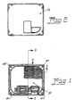
- FIGs. 1 and 2 there is shown in Figs. 1 and 2 an electronic assembly that comprises a housing having a first half 10 and a second half 12.
- the first half 10 and the second half 12 are substantially quadrangular in configuration and each includes concave portions 14, 16, respectively.
- a peripheral groove 18 is formed in the second half 12 and has an O-ring 20 positioned therein.
- At least one first upstanding wall 24 is formed in the first half 10 and at least one second upstanding wall 26 is formed in the second half 12, the walls being in opposition to one another and defining a space therebetween.
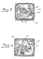
- Fig. 5 two such walls 24 and 26 are shown.
- a first peripheral electrical conductor 34 is formed on the first surface 30 and a second peripheral electrical conductor 36 is formed on the second surface 32.
- the peripheral electrical conductors are in contact with the first upstanding wall 24 and the second upstanding wall 26.
- At least one electrical conductor 38 extends through the printed circuit board 28 and is in electrical contact with the peripheral electrical conductors 34, 36 formed on the first and second surfaces 30, 32.
- a plurality of retainers 40 which can be externally threaded bolts, pass through the first half and into the second half, applying pressure to the printed circuit board for maintaining the printed circuit board in its desired location, thereby eliminating the need for separate screws or other holding devices to hold the printed circuit board in position and greatly reducing mechanical stresses on the board and the components carried thereon. Electromagnetic interference is suppressed by virtue of the contact between the peripheral electrical conductors 34,36 and the first and second halves 10, 12.
- the printed circuit board 28 includes at least one heat-generating component 42, (see Fig. 6 ) and the heat-generating component 42 has thermal transferring media 44, 46 placed between the component 42 and the printed circuit board.
- the heat-generating component can be a power conditioning, semiconductor such as a MOSFET, for example and the thermal transferring media can be a deformable thermal putty.
- the printed circuit board 28 additionally includes electrical components 48, 50 and these electrical components are isolated from the first and second housing halves by air gaps 52, 54, as shown in Fig. 5 .
- the printed circuit board 28 may contain a ferrite component 56 which may comprises two halves 58, 60, the halves 58, 60 being joined together by a spring clip 62 that includes at least two leaf springs 64 in contact with a surface of one of said first housing half or said second housing half.
- the spring clips 64 engage a surface 66 in the second half 12.
- an electronic assembly having reduced mechanical stress in an included printed circuit board, good heat and electrical isolation where necessary and superior EMI suppression, the latter stemming from the portion of a Faraday cage created when the two perimeter conductors 34, 36 and the copper connector 38 that extends between them are contacted by the first half 10 and the second half 12.
Landscapes
- Engineering & Computer Science (AREA)
- Microelectronics & Electronic Packaging (AREA)
- Physics & Mathematics (AREA)
- Thermal Sciences (AREA)
- Shielding Devices Or Components To Electric Or Magnetic Fields (AREA)
- Casings For Electric Apparatus (AREA)
- Cooling Or The Like Of Electrical Apparatus (AREA)
- Arrangement Of Elements, Cooling, Sealing, Or The Like Of Lighting Devices (AREA)
- Circuit Arrangements For Discharge Lamps (AREA)
- Dry Shavers And Clippers (AREA)
- Adhesives Or Adhesive Processes (AREA)
- Electrotherapy Devices (AREA)
Claims (3)
- Ensemble électronique comprenant :un compartiment ayant une première moitié ( 10 ) et une deuxième moitié ( 12 ), la première moitié ( 10 ) et la deuxième moitié ( 12 ) étant sensiblement parallélépipédiques de configuration et comprenant des parties ( 14, 16 ) concaves ;une rainure ( 18 ) périphérique formée dans la deuxième moitié ( 12 ) ;un joint ( 20 ) torique placé dans la rainure ( 18 ) ;une bride ( 22 ) périphérique pendante, formée sur la première moitié ( 10 ) pour coopérer avec le joint ( 20 ) torique lorsque les moitiés ( 10, 12 ) sont appariées ;au moins une première paroi ( 24 ) montante formée dans la première moitié ( 10 ) et au moins une deuxième paroi ( 26 ) montante formée dans la deuxième moitié ( 12 ), les parois ( 24, 26 ) étant en opposition l'une à l'autre et définissant un espace entre elles ;une plaquette ( 28 ) à circuit imprimé placée entre la paroi ( 24 ) dans la première moitié ( 10 ) et la paroi ( 26 ) dans la deuxième moitié ( 12 ), la plaquette ( 28 ) à circuit imprimé ayant des première et deuxième surfaces ( 30, 32 ) ;un conducteur ( 34, 36 ) électrique périphérique formé sur chacune des première et deuxième surfaces ( 30, 32 ) et en contact avec la première paroi ( 24 ) montante et la deuxième paroi ( 26 ) montante ;au moins un conducteur ( 38 ) électrique traversant la plaquette ( 28 ) à circuit imprimé et en contact électrique avec des conducteurs ( 34, 36 ) électriques périphériques formés sur la première et la deuxième surfaces ( 30, 32 ) ; et une pluralité d'arrêtoirs ( 40 ) passant dans la première moitié ( 10 ) et allant dans la deuxième moitié ( 12 ), une pression étant appliquée à la plaquette ( 28 ) à circuit imprimé pour maintenir la plaquette à circuit imprimé dans son emplacement souhaité et une interférence électromagnétique étant supprimée en raison du contact entre les conducteurs ( 34, 36 ) périphériques et les première et deuxième moitiés ( 10, 12 ),caractérisé ence que la plaquette ( 28 ) à circuit imprimé contient un composant ( 56 ) de ferrite comprenant deux moitiés ( 58, 60 ), les moitiés ( 58, 60 ) étant réunies en une agrafe ( 62 ) élastique, qui comprend au moins deux ressorts ( 64 ) à lame en contact avec une surface de l'une de la première moitié ( 10 ) de compartiment ou de la deuxième moitié ( 12 ) de compartiment.
- Ensemble électronique suivant la revendication 1, dans lequel la plaquette ( 28 ) à circuit imprimé comprend au moins un composant ( 42 ) produisant de la chaleur, le composant ( 42 ) produisant de la chaleur ayant des agents ( 44, 46 ) déformables de transfert thermique placés en couplant de manière intime le composant ( 4 ) et l'enceinte.
- Ensemble électronique suivant la revendication 1, dans lequel la plaquette ( 28 ) à circuit imprimé comprend des composants ( 48, 50 ) électriques et les composants électriques sont isolés des première et deuxième moitiés ( 10, 12 ) de compartiment par des intervalles ( 52, 54 ) d'air.
Applications Claiming Priority (3)
| Application Number | Priority Date | Filing Date | Title |
|---|---|---|---|
| US50852003P | 2003-10-03 | 2003-10-03 | |
| US508520P | 2003-10-03 | ||
| PCT/US2004/032528 WO2005034589A2 (fr) | 2003-10-03 | 2004-10-04 | Compartiment pour ballast electronique |
Publications (3)
| Publication Number | Publication Date |
|---|---|
| EP1574118A2 EP1574118A2 (fr) | 2005-09-14 |
| EP1574118A4 EP1574118A4 (fr) | 2008-11-26 |
| EP1574118B1 true EP1574118B1 (fr) | 2010-04-14 |
Family
ID=34421750
Family Applications (1)
| Application Number | Title | Priority Date | Filing Date |
|---|---|---|---|
| EP04794032A Expired - Lifetime EP1574118B1 (fr) | 2003-10-03 | 2004-10-04 | Compartiment pour ballast electronique |
Country Status (11)
| Country | Link |
|---|---|
| US (1) | US8139376B2 (fr) |
| EP (1) | EP1574118B1 (fr) |
| JP (1) | JP4616265B2 (fr) |
| KR (1) | KR101141339B1 (fr) |
| CN (1) | CN100508712C (fr) |
| AT (1) | ATE464778T1 (fr) |
| CA (1) | CA2506528A1 (fr) |
| DE (1) | DE602004026536D1 (fr) |
| RU (1) | RU2348123C2 (fr) |
| TW (1) | TWI333805B (fr) |
| WO (1) | WO2005034589A2 (fr) |
Families Citing this family (14)
| Publication number | Priority date | Publication date | Assignee | Title |
|---|---|---|---|---|
| US7503790B2 (en) * | 2007-07-03 | 2009-03-17 | Rockwell Automation Technologies, Inc. | Industrial automation input output module with elastomeric sealing |
| CN101573022B (zh) * | 2009-06-17 | 2011-08-31 | 杭州华三通信技术有限公司 | 密闭盒体中的散热结构装置及其加工方法 |
| DE102009040573A1 (de) | 2009-09-08 | 2011-03-10 | Osram Gesellschaft mit beschränkter Haftung | Gehäuse für ein Vorschaltgerät |
| JP5177710B2 (ja) * | 2009-10-15 | 2013-04-10 | 株式会社デンソー | 電子制御装置 |
| JP2013105766A (ja) * | 2011-11-10 | 2013-05-30 | Mitsubishi Electric Corp | 電子制御装置 |
| KR101407154B1 (ko) * | 2013-05-10 | 2014-06-13 | 현대오트론 주식회사 | 차량의 전자제어장치 |
| KR101469826B1 (ko) * | 2013-05-10 | 2014-12-05 | 현대오트론 주식회사 | 차량의 전자 제어 장치 |
| FR3030998A1 (fr) * | 2014-12-19 | 2016-06-24 | Sagemcom Broadband Sas | Dispositif electronique pourvu d'un blindage integre a un dissipateur thermique |
| US10120423B1 (en) * | 2015-09-09 | 2018-11-06 | Amazon Technologies, Inc. | Unibody thermal enclosure |
| CN105392318A (zh) * | 2015-12-14 | 2016-03-09 | 武汉元丰汽车电控系统有限公司 | 一种应用于汽车防抱死制动系统的密封壳 |
| JP6834513B2 (ja) * | 2017-01-19 | 2021-02-24 | アイシン精機株式会社 | プリント基板の収容ケース |
| JP2020194922A (ja) * | 2019-05-29 | 2020-12-03 | 京セラ株式会社 | 電子機器及び電子機器製造方法 |
| JP7419050B2 (ja) * | 2019-12-16 | 2024-01-22 | 日立Astemo株式会社 | パワーモジュール、電力変換装置、およびパワーモジュールの製造方法 |
| CN118232252A (zh) * | 2022-12-20 | 2024-06-21 | 苏州力特奥维斯保险丝有限公司 | 高电压pdu设计 |
Family Cites Families (51)
| Publication number | Priority date | Publication date | Assignee | Title |
|---|---|---|---|---|
| US2166003A (en) * | 1937-02-11 | 1939-07-11 | Duncan Electric Mfg Co | Polyphase meter case |
| US5428266A (en) * | 1980-08-14 | 1995-06-27 | Nilssen; Ole K. | Electronic ballast with leakage transformer |
| US4414851A (en) * | 1981-08-28 | 1983-11-15 | Motorola, Inc. | Gauge pressure sensor |
| SU1035848A1 (ru) | 1982-01-19 | 1983-08-15 | Институт Проблем Прочности Ан Усср | Герметичный контейнер,преимущественно дл гидрофизического прибора |
| JPS6090817U (ja) * | 1983-11-29 | 1985-06-21 | 東芝オ−デイオ・ビデオエンジニアリング株式会社 | トランス装置 |
| JPH0644679B2 (ja) | 1986-12-23 | 1994-06-08 | 富士通株式会社 | 高周波回路装置のシ−ルド構造 |
| US4910434A (en) * | 1988-03-31 | 1990-03-20 | Digital Equipment Corporation | Multifunctional enclosure for wiring board in display |
| US4851609A (en) * | 1988-05-10 | 1989-07-25 | Prabhakara Reddy | Protective housing for an electrical device |
| US4879629A (en) * | 1988-10-31 | 1989-11-07 | Unisys Corporation | Liquid cooled multi-chip integrated circuit module incorporating a seamless compliant member for leakproof operation |
| JP2612339B2 (ja) * | 1989-04-18 | 1997-05-21 | 三菱電機株式会社 | 電子機器筐体 |
| SU1807837A1 (ru) | 1990-12-19 | 1995-07-25 | Научно-производственное объединение "Персей" | Герметичный радиоэлектронный блок |
| US5179506A (en) * | 1991-04-01 | 1993-01-12 | Motorola Lighting, Inc. | Securing component arrangement |
| US5418685A (en) * | 1992-02-21 | 1995-05-23 | Robert Bosch Gmbh | Housing for a control device having a printed circuit board with an electrically and thermally conducting lining |
| US5920984A (en) * | 1993-12-10 | 1999-07-13 | Ericsson Ge Mobile Communications Inc. | Method for the suppression of electromagnetic interference in an electronic system |
| US5566055A (en) * | 1995-03-03 | 1996-10-15 | Parker-Hannifin Corporation | Shieled enclosure for electronics |
| EP0840644B1 (fr) * | 1995-07-18 | 1999-04-28 | Parker-Hannifin Corporation | Element de filtration conducteur |
| DE19528632A1 (de) | 1995-08-04 | 1997-02-06 | Bosch Gmbh Robert | Steuergerät bestehend aus mindestens zwei Gehäuseteilen |
| JPH0958162A (ja) * | 1995-08-18 | 1997-03-04 | Mitsubishi Electric Corp | Icカードとその製造法 |
| US6091199A (en) * | 1997-07-30 | 2000-07-18 | Energy Savings, Inc. | Heat spreader for electronic ballast |
| US6090728A (en) | 1998-05-01 | 2000-07-18 | 3M Innovative Properties Company | EMI shielding enclosures |
| US6239359B1 (en) * | 1999-05-11 | 2001-05-29 | Lucent Technologies, Inc. | Circuit board RF shielding |
| DE19921928C2 (de) * | 1999-05-12 | 2002-11-14 | Bosch Gmbh Robert | Elektrisches Gerät |
| JP2001126593A (ja) * | 1999-08-18 | 2001-05-11 | Auto Network Gijutsu Kenkyusho:Kk | ブレーカ装置 |
| US6407925B1 (en) * | 1999-09-17 | 2002-06-18 | Denso Corporation | Casing for electronic control devices |
| JP3498024B2 (ja) | 1999-11-18 | 2004-02-16 | Tdk株式会社 | トランスの放熱構造 |
| JP3648119B2 (ja) * | 2000-03-01 | 2005-05-18 | 株式会社ケーヒン | 電子回路基板の収容ケース |
| US6433492B1 (en) * | 2000-09-18 | 2002-08-13 | Northrop Grumman Corporation | Magnetically shielded electrodeless light source |
| JP2002222720A (ja) * | 2001-01-24 | 2002-08-09 | Kawaguchiko Seimitsu Co Ltd | 表面実装型小型トランス |
| US6717051B2 (en) * | 2001-02-21 | 2004-04-06 | Denso Corporation | Electronic control unit for use in automotive vehicle |
| TW511453B (en) | 2001-05-21 | 2002-11-21 | Yin King Ind Co Ltd | EMI preventing device and its manufacturing method |
| DE10126189C2 (de) * | 2001-05-30 | 2003-12-18 | Bosch Gmbh Robert | Gehäuse für ein elektrisches Gerät, insbesondere ein Schalt-oder Steuergerät in einem KFZ |
| JP2003036985A (ja) * | 2001-07-25 | 2003-02-07 | Matsushita Electric Works Ltd | 放電灯点灯装置 |
| US7230823B2 (en) * | 2003-08-20 | 2007-06-12 | Otter Products, Llc | Protective membrane for touch screen device |
| CN2511095Y (zh) | 2001-11-23 | 2002-09-11 | 杜昆洪 | 电子镇流器外壳 |
| CN2523169Y (zh) * | 2001-11-29 | 2002-11-27 | 顺德市容桂镇百事利实业有限公司 | 电子镇流器外壳 |
| US6565382B1 (en) * | 2001-12-07 | 2003-05-20 | Hewelett-Packard Development Company, L.P. | Core mounting assembly and clamp therefor |
| DE10162600A1 (de) | 2001-12-20 | 2003-07-10 | Bosch Gmbh Robert | Gehäuseanordnung für ein elektrisches Gerät |
| US20030184981A1 (en) * | 2002-03-29 | 2003-10-02 | Fredrick Daniels | Protective pot or container |
| WO2003096500A1 (fr) * | 2002-05-14 | 2003-11-20 | Sumitomo Electric Industries, Ltd. | Module optique |
| US6707256B2 (en) * | 2002-06-25 | 2004-03-16 | Electronic Theatre Controls, Inc. | Dimmer pack |
| US7218516B2 (en) * | 2004-09-24 | 2007-05-15 | Shuttle, Inc. | Inlet airflow guiding structure for computers |
| US7158384B2 (en) * | 2005-05-09 | 2007-01-02 | Delta Electronics, Inc. | Vibration reducing structure of electronic device |
| JP2007165048A (ja) * | 2005-12-12 | 2007-06-28 | Smc Corp | 信号入出力装置 |
| JP4357504B2 (ja) * | 2006-06-29 | 2009-11-04 | 株式会社日立製作所 | エンジン制御装置 |
| US7420811B2 (en) * | 2006-09-14 | 2008-09-02 | Tsung-Wen Chan | Heat sink structure for light-emitting diode based streetlamp |
| US7563992B2 (en) * | 2006-09-20 | 2009-07-21 | Delphi Technologies, Inc. | Electronic enclosure with continuous ground contact surface |
| TWM315472U (en) * | 2006-11-28 | 2007-07-11 | Microelectronics Tech Inc | Electromagnetic interference shielding apparatus for transmitter |
| US20080169768A1 (en) * | 2007-01-16 | 2008-07-17 | Kevin Yang | Electronic ballast with PCB edge mounted output transformer/inductor |
| US7503790B2 (en) | 2007-07-03 | 2009-03-17 | Rockwell Automation Technologies, Inc. | Industrial automation input output module with elastomeric sealing |
| JP4426610B2 (ja) * | 2007-08-28 | 2010-03-03 | 株式会社日立コミュニケーションテクノロジー | 電子装置 |
| US7656649B2 (en) * | 2007-12-26 | 2010-02-02 | Elster Electricity, Llc | Mechanical packaging apparatus and methods for an electrical energy meter |
-
2004
- 2004-10-01 TW TW093129829A patent/TWI333805B/zh not_active IP Right Cessation
- 2004-10-04 AT AT04794032T patent/ATE464778T1/de not_active IP Right Cessation
- 2004-10-04 CN CNB2004800012766A patent/CN100508712C/zh not_active Expired - Fee Related
- 2004-10-04 CA CA002506528A patent/CA2506528A1/fr not_active Abandoned
- 2004-10-04 US US12/279,593 patent/US8139376B2/en not_active Expired - Fee Related
- 2004-10-04 DE DE602004026536T patent/DE602004026536D1/de not_active Expired - Lifetime
- 2004-10-04 WO PCT/US2004/032528 patent/WO2005034589A2/fr not_active Ceased
- 2004-10-04 EP EP04794032A patent/EP1574118B1/fr not_active Expired - Lifetime
- 2004-10-04 RU RU2005115090/09A patent/RU2348123C2/ru not_active IP Right Cessation
- 2004-10-04 JP JP2006534198A patent/JP4616265B2/ja not_active Expired - Fee Related
- 2004-10-04 KR KR1020057008960A patent/KR101141339B1/ko not_active Expired - Fee Related
Also Published As
| Publication number | Publication date |
|---|---|
| ATE464778T1 (de) | 2010-04-15 |
| TW200515844A (en) | 2005-05-01 |
| RU2348123C2 (ru) | 2009-02-27 |
| WO2005034589A2 (fr) | 2005-04-14 |
| US8139376B2 (en) | 2012-03-20 |
| US20100259901A1 (en) | 2010-10-14 |
| CA2506528A1 (fr) | 2005-04-14 |
| EP1574118A4 (fr) | 2008-11-26 |
| TWI333805B (en) | 2010-11-21 |
| JP4616265B2 (ja) | 2011-01-19 |
| KR101141339B1 (ko) | 2012-05-03 |
| CN100508712C (zh) | 2009-07-01 |
| WO2005034589A3 (fr) | 2005-06-16 |
| KR20060112588A (ko) | 2006-11-01 |
| CN1706234A (zh) | 2005-12-07 |
| DE602004026536D1 (fr) | 2010-05-27 |
| RU2005115090A (ru) | 2006-03-10 |
| JP2007507854A (ja) | 2007-03-29 |
| EP1574118A2 (fr) | 2005-09-14 |
Similar Documents
| Publication | Publication Date | Title |
|---|---|---|
| EP1574118B1 (fr) | Compartiment pour ballast electronique | |
| CN108336892B (zh) | 电源模块及其组装结构与组装方法 | |
| US6044899A (en) | Low EMI emissions heat sink device | |
| US8116099B2 (en) | Circuit board device, electronic device provided with the same, and GND connecting method | |
| EP2685564B1 (fr) | Module électronique et méthode de préparation d'un module électronique | |
| IL130775A (en) | Conduction cooled electronic card module and method of producing the same utilizing an electronic circuit card originally designed for convection cooling | |
| WO2002013315A3 (fr) | Connecteur electronique a forte conductivite thermique | |
| US20220408569A1 (en) | Electronic control device | |
| KR101326907B1 (ko) | 전기 장치 | |
| KR20220133192A (ko) | Emc 필터 플러그인 장치 | |
| US11769961B2 (en) | Electrical connector module and heat dissipation housing | |
| US7061774B2 (en) | Computer board with dual shield housing and heat sink expansion zone apparatuses | |
| CN1102331C (zh) | 电装置 | |
| JP5463203B2 (ja) | 電子制御装置 | |
| CN104113029B (zh) | 建筑布线技术的电子暗装设备 | |
| KR101063172B1 (ko) | 전자제어장치 | |
| CN108988614B (zh) | 用于连接电端子的系统 | |
| JP5072522B2 (ja) | 接続構造 | |
| CN102960079B (zh) | 具有由成型材料构成的壳体的电子设备 | |
| WO2001069987A2 (fr) | Plaquette de circuits imprimes a performances thermiques ameliorees | |
| JPH1041602A (ja) | 高周波回路基板の取り付け構造 | |
| NZ530070A (en) | Electric connection arrangement for electronic devices | |
| CN119110539A (zh) | 一种降低开关电源共模电流的功率管散热器 | |
| CN121077227A (zh) | 电磁兼容性emc滤波器、电路装置以及电源管理系统 | |
| JP2005237183A (ja) | トランスの放熱ができるスイッチング電源装置 |
Legal Events
| Date | Code | Title | Description |
|---|---|---|---|
| PUAI | Public reference made under article 153(3) epc to a published international application that has entered the european phase |
Free format text: ORIGINAL CODE: 0009012 |
|
| 17P | Request for examination filed |
Effective date: 20050518 |
|
| AK | Designated contracting states |
Kind code of ref document: A2 Designated state(s): AT BE BG CH CY CZ DE DK EE ES FI FR GB GR HU IE IT LI LU MC NL PL PT RO SE SI SK TR |
|
| AX | Request for extension of the european patent |
Extension state: AL HR LT LV MK |
|
| A4 | Supplementary search report drawn up and despatched |
Effective date: 20081029 |
|
| 17Q | First examination report despatched |
Effective date: 20090408 |
|
| GRAP | Despatch of communication of intention to grant a patent |
Free format text: ORIGINAL CODE: EPIDOSNIGR1 |
|
| GRAS | Grant fee paid |
Free format text: ORIGINAL CODE: EPIDOSNIGR3 |
|
| GRAA | (expected) grant |
Free format text: ORIGINAL CODE: 0009210 |
|
| AK | Designated contracting states |
Kind code of ref document: B1 Designated state(s): AT BE BG CH CY CZ DE DK EE ES FI FR GB GR HU IE IT LI LU MC NL PL PT RO SE SI SK TR |
|
| AX | Request for extension of the european patent |
Extension state: AL HR LT LV MK |
|
| REG | Reference to a national code |
Ref country code: GB Ref legal event code: FG4D |
|
| REG | Reference to a national code |
Ref country code: CH Ref legal event code: EP |
|
| REG | Reference to a national code |
Ref country code: IE Ref legal event code: FG4D |
|
| REF | Corresponds to: |
Ref document number: 602004026536 Country of ref document: DE Date of ref document: 20100527 Kind code of ref document: P |
|
| REG | Reference to a national code |
Ref country code: NL Ref legal event code: VDEP Effective date: 20100414 |
|
| LTIE | Lt: invalidation of european patent or patent extension |
Effective date: 20100414 |
|
| PG25 | Lapsed in a contracting state [announced via postgrant information from national office to epo] |
Ref country code: SE Free format text: LAPSE BECAUSE OF FAILURE TO SUBMIT A TRANSLATION OF THE DESCRIPTION OR TO PAY THE FEE WITHIN THE PRESCRIBED TIME-LIMIT Effective date: 20100414 Ref country code: ES Free format text: LAPSE BECAUSE OF FAILURE TO SUBMIT A TRANSLATION OF THE DESCRIPTION OR TO PAY THE FEE WITHIN THE PRESCRIBED TIME-LIMIT Effective date: 20100725 Ref country code: NL Free format text: LAPSE BECAUSE OF FAILURE TO SUBMIT A TRANSLATION OF THE DESCRIPTION OR TO PAY THE FEE WITHIN THE PRESCRIBED TIME-LIMIT Effective date: 20100414 |
|
| PG25 | Lapsed in a contracting state [announced via postgrant information from national office to epo] |
Ref country code: FI Free format text: LAPSE BECAUSE OF FAILURE TO SUBMIT A TRANSLATION OF THE DESCRIPTION OR TO PAY THE FEE WITHIN THE PRESCRIBED TIME-LIMIT Effective date: 20100414 Ref country code: AT Free format text: LAPSE BECAUSE OF FAILURE TO SUBMIT A TRANSLATION OF THE DESCRIPTION OR TO PAY THE FEE WITHIN THE PRESCRIBED TIME-LIMIT Effective date: 20100414 Ref country code: SI Free format text: LAPSE BECAUSE OF FAILURE TO SUBMIT A TRANSLATION OF THE DESCRIPTION OR TO PAY THE FEE WITHIN THE PRESCRIBED TIME-LIMIT Effective date: 20100414 |
|
| PG25 | Lapsed in a contracting state [announced via postgrant information from national office to epo] |
Ref country code: PL Free format text: LAPSE BECAUSE OF FAILURE TO SUBMIT A TRANSLATION OF THE DESCRIPTION OR TO PAY THE FEE WITHIN THE PRESCRIBED TIME-LIMIT Effective date: 20100414 Ref country code: CY Free format text: LAPSE BECAUSE OF FAILURE TO SUBMIT A TRANSLATION OF THE DESCRIPTION OR TO PAY THE FEE WITHIN THE PRESCRIBED TIME-LIMIT Effective date: 20100421 Ref country code: GR Free format text: LAPSE BECAUSE OF FAILURE TO SUBMIT A TRANSLATION OF THE DESCRIPTION OR TO PAY THE FEE WITHIN THE PRESCRIBED TIME-LIMIT Effective date: 20100715 |
|
| PG25 | Lapsed in a contracting state [announced via postgrant information from national office to epo] |
Ref country code: DK Free format text: LAPSE BECAUSE OF FAILURE TO SUBMIT A TRANSLATION OF THE DESCRIPTION OR TO PAY THE FEE WITHIN THE PRESCRIBED TIME-LIMIT Effective date: 20100414 Ref country code: EE Free format text: LAPSE BECAUSE OF FAILURE TO SUBMIT A TRANSLATION OF THE DESCRIPTION OR TO PAY THE FEE WITHIN THE PRESCRIBED TIME-LIMIT Effective date: 20100414 Ref country code: PT Free format text: LAPSE BECAUSE OF FAILURE TO SUBMIT A TRANSLATION OF THE DESCRIPTION OR TO PAY THE FEE WITHIN THE PRESCRIBED TIME-LIMIT Effective date: 20100816 |
|
| PLBE | No opposition filed within time limit |
Free format text: ORIGINAL CODE: 0009261 |
|
| STAA | Information on the status of an ep patent application or granted ep patent |
Free format text: STATUS: NO OPPOSITION FILED WITHIN TIME LIMIT |
|
| PG25 | Lapsed in a contracting state [announced via postgrant information from national office to epo] |
Ref country code: RO Free format text: LAPSE BECAUSE OF FAILURE TO SUBMIT A TRANSLATION OF THE DESCRIPTION OR TO PAY THE FEE WITHIN THE PRESCRIBED TIME-LIMIT Effective date: 20100414 Ref country code: CZ Free format text: LAPSE BECAUSE OF FAILURE TO SUBMIT A TRANSLATION OF THE DESCRIPTION OR TO PAY THE FEE WITHIN THE PRESCRIBED TIME-LIMIT Effective date: 20100414 Ref country code: SK Free format text: LAPSE BECAUSE OF FAILURE TO SUBMIT A TRANSLATION OF THE DESCRIPTION OR TO PAY THE FEE WITHIN THE PRESCRIBED TIME-LIMIT Effective date: 20100414 Ref country code: BE Free format text: LAPSE BECAUSE OF FAILURE TO SUBMIT A TRANSLATION OF THE DESCRIPTION OR TO PAY THE FEE WITHIN THE PRESCRIBED TIME-LIMIT Effective date: 20100414 |
|
| 26N | No opposition filed |
Effective date: 20110117 |
|
| PG25 | Lapsed in a contracting state [announced via postgrant information from national office to epo] |
Ref country code: MC Free format text: LAPSE BECAUSE OF NON-PAYMENT OF DUE FEES Effective date: 20101031 |
|
| REG | Reference to a national code |
Ref country code: CH Ref legal event code: PL |
|
| PG25 | Lapsed in a contracting state [announced via postgrant information from national office to epo] |
Ref country code: LI Free format text: LAPSE BECAUSE OF NON-PAYMENT OF DUE FEES Effective date: 20101031 Ref country code: CH Free format text: LAPSE BECAUSE OF NON-PAYMENT OF DUE FEES Effective date: 20101031 |
|
| PG25 | Lapsed in a contracting state [announced via postgrant information from national office to epo] |
Ref country code: IE Free format text: LAPSE BECAUSE OF NON-PAYMENT OF DUE FEES Effective date: 20101004 |
|
| PG25 | Lapsed in a contracting state [announced via postgrant information from national office to epo] |
Ref country code: LU Free format text: LAPSE BECAUSE OF NON-PAYMENT OF DUE FEES Effective date: 20101004 Ref country code: HU Free format text: LAPSE BECAUSE OF FAILURE TO SUBMIT A TRANSLATION OF THE DESCRIPTION OR TO PAY THE FEE WITHIN THE PRESCRIBED TIME-LIMIT Effective date: 20101015 Ref country code: BG Free format text: LAPSE BECAUSE OF FAILURE TO SUBMIT A TRANSLATION OF THE DESCRIPTION OR TO PAY THE FEE WITHIN THE PRESCRIBED TIME-LIMIT Effective date: 20100414 |
|
| PG25 | Lapsed in a contracting state [announced via postgrant information from national office to epo] |
Ref country code: TR Free format text: LAPSE BECAUSE OF FAILURE TO SUBMIT A TRANSLATION OF THE DESCRIPTION OR TO PAY THE FEE WITHIN THE PRESCRIBED TIME-LIMIT Effective date: 20100414 |
|
| PG25 | Lapsed in a contracting state [announced via postgrant information from national office to epo] |
Ref country code: BG Free format text: LAPSE BECAUSE OF FAILURE TO SUBMIT A TRANSLATION OF THE DESCRIPTION OR TO PAY THE FEE WITHIN THE PRESCRIBED TIME-LIMIT Effective date: 20100714 |
|
| REG | Reference to a national code |
Ref country code: FR Ref legal event code: PLFP Year of fee payment: 12 |
|
| REG | Reference to a national code |
Ref country code: FR Ref legal event code: PLFP Year of fee payment: 13 |
|
| REG | Reference to a national code |
Ref country code: FR Ref legal event code: PLFP Year of fee payment: 14 |
|
| PGFP | Annual fee paid to national office [announced via postgrant information from national office to epo] |
Ref country code: FR Payment date: 20171024 Year of fee payment: 14 Ref country code: DE Payment date: 20171019 Year of fee payment: 14 |
|
| PGFP | Annual fee paid to national office [announced via postgrant information from national office to epo] |
Ref country code: IT Payment date: 20171023 Year of fee payment: 14 Ref country code: GB Payment date: 20171019 Year of fee payment: 14 |
|
| REG | Reference to a national code |
Ref country code: DE Ref legal event code: R119 Ref document number: 602004026536 Country of ref document: DE |
|
| GBPC | Gb: european patent ceased through non-payment of renewal fee |
Effective date: 20181004 |
|
| PG25 | Lapsed in a contracting state [announced via postgrant information from national office to epo] |
Ref country code: DE Free format text: LAPSE BECAUSE OF NON-PAYMENT OF DUE FEES Effective date: 20190501 |
|
| PG25 | Lapsed in a contracting state [announced via postgrant information from national office to epo] |
Ref country code: FR Free format text: LAPSE BECAUSE OF NON-PAYMENT OF DUE FEES Effective date: 20181031 |
|
| PG25 | Lapsed in a contracting state [announced via postgrant information from national office to epo] |
Ref country code: IT Free format text: LAPSE BECAUSE OF NON-PAYMENT OF DUE FEES Effective date: 20181004 Ref country code: GB Free format text: LAPSE BECAUSE OF NON-PAYMENT OF DUE FEES Effective date: 20181004 |