EP1571716A1 - Light-emitting device - Google Patents
Light-emitting device Download PDFInfo
- Publication number
- EP1571716A1 EP1571716A1 EP04771196A EP04771196A EP1571716A1 EP 1571716 A1 EP1571716 A1 EP 1571716A1 EP 04771196 A EP04771196 A EP 04771196A EP 04771196 A EP04771196 A EP 04771196A EP 1571716 A1 EP1571716 A1 EP 1571716A1
- Authority
- EP
- European Patent Office
- Prior art keywords
- light emitting
- layer
- nitride semiconductor
- type
- substrate
- Prior art date
- Legal status (The legal status is an assumption and is not a legal conclusion. Google has not performed a legal analysis and makes no representation as to the accuracy of the status listed.)
- Withdrawn
Links
Images










Classifications
-
- H—ELECTRICITY
- H10—SEMICONDUCTOR DEVICES; ELECTRIC SOLID-STATE DEVICES NOT OTHERWISE PROVIDED FOR
- H10H—INORGANIC LIGHT-EMITTING SEMICONDUCTOR DEVICES HAVING POTENTIAL BARRIERS
- H10H20/00—Individual inorganic light-emitting semiconductor devices having potential barriers, e.g. light-emitting diodes [LED]
- H10H20/80—Constructional details
- H10H20/81—Bodies
- H10H20/822—Materials of the light-emitting regions
- H10H20/824—Materials of the light-emitting regions comprising only Group III-V materials, e.g. GaP
- H10H20/825—Materials of the light-emitting regions comprising only Group III-V materials, e.g. GaP containing nitrogen, e.g. GaN
-
- H—ELECTRICITY
- H10—SEMICONDUCTOR DEVICES; ELECTRIC SOLID-STATE DEVICES NOT OTHERWISE PROVIDED FOR
- H10H—INORGANIC LIGHT-EMITTING SEMICONDUCTOR DEVICES HAVING POTENTIAL BARRIERS
- H10H20/00—Individual inorganic light-emitting semiconductor devices having potential barriers, e.g. light-emitting diodes [LED]
- H10H20/80—Constructional details
- H10H20/81—Bodies
- H10H20/819—Bodies characterised by their shape, e.g. curved or truncated substrates
-
- H—ELECTRICITY
- H10—SEMICONDUCTOR DEVICES; ELECTRIC SOLID-STATE DEVICES NOT OTHERWISE PROVIDED FOR
- H10H—INORGANIC LIGHT-EMITTING SEMICONDUCTOR DEVICES HAVING POTENTIAL BARRIERS
- H10H20/00—Individual inorganic light-emitting semiconductor devices having potential barriers, e.g. light-emitting diodes [LED]
- H10H20/80—Constructional details
- H10H20/83—Electrodes
- H10H20/831—Electrodes characterised by their shape
- H10H20/8312—Electrodes characterised by their shape extending at least partially through the bodies
-
- H—ELECTRICITY
- H10—SEMICONDUCTOR DEVICES; ELECTRIC SOLID-STATE DEVICES NOT OTHERWISE PROVIDED FOR
- H10H—INORGANIC LIGHT-EMITTING SEMICONDUCTOR DEVICES HAVING POTENTIAL BARRIERS
- H10H20/00—Individual inorganic light-emitting semiconductor devices having potential barriers, e.g. light-emitting diodes [LED]
- H10H20/80—Constructional details
- H10H20/85—Packages
- H10H20/851—Wavelength conversion means
- H10H20/8514—Wavelength conversion means characterised by their shape, e.g. plate or foil
-
- H—ELECTRICITY
- H10—SEMICONDUCTOR DEVICES; ELECTRIC SOLID-STATE DEVICES NOT OTHERWISE PROVIDED FOR
- H10H—INORGANIC LIGHT-EMITTING SEMICONDUCTOR DEVICES HAVING POTENTIAL BARRIERS
- H10H20/00—Individual inorganic light-emitting semiconductor devices having potential barriers, e.g. light-emitting diodes [LED]
- H10H20/80—Constructional details
- H10H20/85—Packages
- H10H20/851—Wavelength conversion means
- H10H20/8515—Wavelength conversion means not being in contact with the bodies
-
- H—ELECTRICITY
- H10—SEMICONDUCTOR DEVICES; ELECTRIC SOLID-STATE DEVICES NOT OTHERWISE PROVIDED FOR
- H10H—INORGANIC LIGHT-EMITTING SEMICONDUCTOR DEVICES HAVING POTENTIAL BARRIERS
- H10H20/00—Individual inorganic light-emitting semiconductor devices having potential barriers, e.g. light-emitting diodes [LED]
- H10H20/80—Constructional details
- H10H20/85—Packages
- H10H20/855—Optical field-shaping means, e.g. lenses
-
- H—ELECTRICITY
- H10—SEMICONDUCTOR DEVICES; ELECTRIC SOLID-STATE DEVICES NOT OTHERWISE PROVIDED FOR
- H10W—GENERIC PACKAGES, INTERCONNECTIONS, CONNECTORS OR OTHER CONSTRUCTIONAL DETAILS OF DEVICES COVERED BY CLASS H10
- H10W72/00—Interconnections or connectors in packages
- H10W72/01—Manufacture or treatment
- H10W72/015—Manufacture or treatment of bond wires
- H10W72/01515—Forming coatings
-
- H—ELECTRICITY
- H10—SEMICONDUCTOR DEVICES; ELECTRIC SOLID-STATE DEVICES NOT OTHERWISE PROVIDED FOR
- H10W—GENERIC PACKAGES, INTERCONNECTIONS, CONNECTORS OR OTHER CONSTRUCTIONAL DETAILS OF DEVICES COVERED BY CLASS H10
- H10W72/00—Interconnections or connectors in packages
- H10W72/071—Connecting or disconnecting
- H10W72/072—Connecting or disconnecting of bump connectors
- H10W72/07251—Connecting or disconnecting of bump connectors characterised by changes in properties of the bump connectors during connecting
- H10W72/07252—Connecting or disconnecting of bump connectors characterised by changes in properties of the bump connectors during connecting changes in structures or sizes
-
- H—ELECTRICITY
- H10—SEMICONDUCTOR DEVICES; ELECTRIC SOLID-STATE DEVICES NOT OTHERWISE PROVIDED FOR
- H10W—GENERIC PACKAGES, INTERCONNECTIONS, CONNECTORS OR OTHER CONSTRUCTIONAL DETAILS OF DEVICES COVERED BY CLASS H10
- H10W72/00—Interconnections or connectors in packages
- H10W72/071—Connecting or disconnecting
- H10W72/075—Connecting or disconnecting of bond wires
-
- H—ELECTRICITY
- H10—SEMICONDUCTOR DEVICES; ELECTRIC SOLID-STATE DEVICES NOT OTHERWISE PROVIDED FOR
- H10W—GENERIC PACKAGES, INTERCONNECTIONS, CONNECTORS OR OTHER CONSTRUCTIONAL DETAILS OF DEVICES COVERED BY CLASS H10
- H10W72/00—Interconnections or connectors in packages
- H10W72/20—Bump connectors, e.g. solder bumps or copper pillars; Dummy bumps; Thermal bumps
- H10W72/221—Structures or relative sizes
- H10W72/227—Multiple bumps having different sizes
-
- H—ELECTRICITY
- H10—SEMICONDUCTOR DEVICES; ELECTRIC SOLID-STATE DEVICES NOT OTHERWISE PROVIDED FOR
- H10W—GENERIC PACKAGES, INTERCONNECTIONS, CONNECTORS OR OTHER CONSTRUCTIONAL DETAILS OF DEVICES COVERED BY CLASS H10
- H10W72/00—Interconnections or connectors in packages
- H10W72/50—Bond wires
- H10W72/551—Materials of bond wires
- H10W72/552—Materials of bond wires comprising metals or metalloids, e.g. silver
-
- H—ELECTRICITY
- H10—SEMICONDUCTOR DEVICES; ELECTRIC SOLID-STATE DEVICES NOT OTHERWISE PROVIDED FOR
- H10W—GENERIC PACKAGES, INTERCONNECTIONS, CONNECTORS OR OTHER CONSTRUCTIONAL DETAILS OF DEVICES COVERED BY CLASS H10
- H10W72/00—Interconnections or connectors in packages
- H10W72/50—Bond wires
- H10W72/551—Materials of bond wires
- H10W72/552—Materials of bond wires comprising metals or metalloids, e.g. silver
- H10W72/5522—Materials of bond wires comprising metals or metalloids, e.g. silver comprising gold [Au]
-
- H—ELECTRICITY
- H10—SEMICONDUCTOR DEVICES; ELECTRIC SOLID-STATE DEVICES NOT OTHERWISE PROVIDED FOR
- H10W—GENERIC PACKAGES, INTERCONNECTIONS, CONNECTORS OR OTHER CONSTRUCTIONAL DETAILS OF DEVICES COVERED BY CLASS H10
- H10W72/00—Interconnections or connectors in packages
- H10W72/851—Dispositions of multiple connectors or interconnections
- H10W72/874—On different surfaces
- H10W72/884—Die-attach connectors and bond wires
-
- H—ELECTRICITY
- H10—SEMICONDUCTOR DEVICES; ELECTRIC SOLID-STATE DEVICES NOT OTHERWISE PROVIDED FOR
- H10W—GENERIC PACKAGES, INTERCONNECTIONS, CONNECTORS OR OTHER CONSTRUCTIONAL DETAILS OF DEVICES COVERED BY CLASS H10
- H10W72/00—Interconnections or connectors in packages
- H10W72/90—Bond pads, in general
-
- H—ELECTRICITY
- H10—SEMICONDUCTOR DEVICES; ELECTRIC SOLID-STATE DEVICES NOT OTHERWISE PROVIDED FOR
- H10W—GENERIC PACKAGES, INTERCONNECTIONS, CONNECTORS OR OTHER CONSTRUCTIONAL DETAILS OF DEVICES COVERED BY CLASS H10
- H10W72/00—Interconnections or connectors in packages
- H10W72/90—Bond pads, in general
- H10W72/941—Dispositions of bond pads
- H10W72/944—Dispositions of multiple bond pads
-
- H—ELECTRICITY
- H10—SEMICONDUCTOR DEVICES; ELECTRIC SOLID-STATE DEVICES NOT OTHERWISE PROVIDED FOR
- H10W—GENERIC PACKAGES, INTERCONNECTIONS, CONNECTORS OR OTHER CONSTRUCTIONAL DETAILS OF DEVICES COVERED BY CLASS H10
- H10W90/00—Package configurations
- H10W90/701—Package configurations characterised by the relative positions of pads or connectors relative to package parts
- H10W90/721—Package configurations characterised by the relative positions of pads or connectors relative to package parts of bump connectors
- H10W90/726—Package configurations characterised by the relative positions of pads or connectors relative to package parts of bump connectors between a chip and a stacked lead frame, conducting package substrate or heat sink
-
- H—ELECTRICITY
- H10—SEMICONDUCTOR DEVICES; ELECTRIC SOLID-STATE DEVICES NOT OTHERWISE PROVIDED FOR
- H10W—GENERIC PACKAGES, INTERCONNECTIONS, CONNECTORS OR OTHER CONSTRUCTIONAL DETAILS OF DEVICES COVERED BY CLASS H10
- H10W90/00—Package configurations
- H10W90/701—Package configurations characterised by the relative positions of pads or connectors relative to package parts
- H10W90/731—Package configurations characterised by the relative positions of pads or connectors relative to package parts of die-attach connectors
- H10W90/736—Package configurations characterised by the relative positions of pads or connectors relative to package parts of die-attach connectors between a chip and a stacked lead frame, conducting package substrate or heat sink
-
- H—ELECTRICITY
- H10—SEMICONDUCTOR DEVICES; ELECTRIC SOLID-STATE DEVICES NOT OTHERWISE PROVIDED FOR
- H10W—GENERIC PACKAGES, INTERCONNECTIONS, CONNECTORS OR OTHER CONSTRUCTIONAL DETAILS OF DEVICES COVERED BY CLASS H10
- H10W90/00—Package configurations
- H10W90/701—Package configurations characterised by the relative positions of pads or connectors relative to package parts
- H10W90/751—Package configurations characterised by the relative positions of pads or connectors relative to package parts of bond wires
- H10W90/756—Package configurations characterised by the relative positions of pads or connectors relative to package parts of bond wires between a chip and a stacked lead frame, conducting package substrate or heat sink
Definitions
- the present invention relates to light emitting apparatuses and more particularly to light emitting apparatuses formed from nitride semiconductors.
- a light emitting apparatus of the present invention refers to a semiconductor device or semiconductor chip mainly constituted by a nitride semiconductor substrate and semiconductor layers laminated thereon in some cases and also refers to a device including a semiconductor chip mounted on a mounting component and sealed with resin in some cases. Also, it may refer to the both in some cases.
- a semiconductor chip is called a chip in some cases.
- a substrate and epitaxial layers formed thereon in a chip are simply called a substrate in some cases.
- LEDs white light emitting diodes
- compact electronic equipment such as portable information terminals
- LEDs have the potentiality to be utilized for illumination for larger spaces or larger areas in the future.
- it is required to increase the light outputs of LEDs. Therefore, there is a need to enable flowing large currents through the electrodes of LEDs and overcome a problem of temperature increases caused by heat generation.
- Fig. 59 illustrates the construction of a GaN-based LED which has been currently proposed (a patent document 1).
- an n-type GaN layer 102 is provided on a sapphire substrate 101 and a quantum-well construction 103 is formed between n-type GaN layer 102 and a p-type GaN layer 104.
- Light emission occurs at quantum-well construction 103.
- a p-electrode 105 is formed to be in ohmic contact and on n-type GaN layer 102 an n-electrode 106 is formed to be in ohmic contact.
- the mounting component is formed from an Si substrate and provided with circuits for protection against surge voltages from the outside.
- the electrical power branching circuit for protecting the light emitting apparatus is constituted by Zener diodes, etc., placing emphasis on that main factors of circuit failure for semiconductor of a nitride of Ga, Al, In or other group III element are surge voltages such as transient voltage and static discharge. Protection against surge voltages will be described in detail later.
- the above GaN-based LED is characterized in that (a1) p-type GaN layer 104 is down-mounted and (a2) n-electrode layer 106 is formed on n-type GaN layer 102 so that light is emitted from the backside of sapphire substrate 101.
- the construction of the GaN-based LED is significantly complicated as can be seen in Fig. 59.
- the reason that (a2) the n-electrode layer is formed on n-type GaN layer 102, which is the cause of such a complicated construction, is that sapphire substrate 101 is an insulator and the n-electrode can not be provided on the sapphire substrate.
- LEDs constructed to emit light from a p-type GaN layer using a laminate construction of (n-electrode on the SiC substrate backside/SiC substrate/n-type GaN layer/quantum-well laminate construction (light emitting layer)/p-type GaN layer/p-electrode) have been also widely utilized.
- n-type GaN layer 102 Furthermore, there is large resistance to currents flowing in the direction parallel to the substrate through n-type GaN layer 102, which causes heat generation and an increase of the driving voltage and, therefore, an increase of the power consumption. Particularly, if the thickness of the n-type GaN layer is reduced in order to shorten the film forming processes, the yield of exposure of the n-type GaN film will be significantly degraded, besides the above problem of heat generation and power consumption increases.
- the heat radiating area is restricted and also the heat resistance (temperature increase caused by unit introduced energy per unit area) is large, the injection current per light emitting apparatus can not be increased.
- the area of the p-electrode is restricted, it is common to heat-design the apparatus with little margin.
- the design of heat conditions is basically important for light emitting apparatuses and when an attempt is made to obtain high outputs, there will be restriction due to heat conditions as above. Therefore, in order to alleviate this as much as possible, a complicated electrode shape must be employed.
- the light emission efficiency at the main surface of the sapphire substrate will be degraded.
- the problem of the light emission efficiency is important, there are still other problems.
- the light experienced the above total internal reflection propagates through the GaN layers and is emitted from the side portions of the GaN layers. Since the ratio of the light which experiences the above total internal reflection is significantly large and also the GaN layers are thin, the energy density of light emitted from the side portions becomes large.
- the sealing resin placed at the side portions of the GaN layers and irradiated with the light is damaged and this causes a problem of shortening the life of the light emitting apparatus.
- GaN-based LED having a construction of (SiC substrate backside n-electrode/SiC substrate/n-type GaN layer/quantum-well laminate construction (light emitting layer)/ p-type GaN layer/ p-electrode) for extracting light from the p-layers side
- the light absorption ratio at the p-electrode is large and thus high light outputs can not be emitted to the outside efficiently.
- currents can not be flowed through the entire p-type GaN layer because of the high electrical resistance of the p-type GaN layer.
- a light emitting apparatus is a light emitting apparatus including a nitride semiconductor substrate, an n-type nitride semiconductor layer at a first main surface side of the nitride semiconductor substrate, a p-type nitride semiconductor layer placed more distantly from the nitride semiconductor substrate than the n-type nitride semiconductor layer at the first main surface side and a light emitting layer placed between the n-type nitride semiconductor layer and the p-type nitride semiconductor layer at the first main surface side.
- the nitride semiconductor substrate has a resistivity of 0.5 ⁇ •cm or less and the p-type nitride semiconductor layer side is down-mounted so that light is emitted from the second main surface of the nitride semiconductor substrate at the opposite side from the first main surface.
- the n-type electrode is provided on the backside (second main surface) of the nitride semiconductor substrate with a low electrical resistance. Therefore, even when the n-electrode is provided with a low coverage ratio or high opening ratio, currents can be flowed through the entire nitride semiconductor substrate. Thus, the light absorption ratio at the emitting surface becomes lower and the light emission efficiency may be increased. Further, it goes without saying that light emission may occur at the side surfaces as well as at the second main surface. The same holds for the following light emitting apparatuses.
- the p-type nitride semiconductor layer side having a high electrical resistance does not form a light emitting surface and therefore the p-type electrode layer may be formed on the entire surface of the p-type nitride semiconductor layer.
- This construction is advantageous in flowing large currents and suppressing heat generation and in discharging generated heat by conduction. Namely, restrictions caused by heat requirements may be drastically alleviated. Thus, there is no need to form a comb-shaped electrode in which the n-electrode and the p-electrode are complicated in order to reduce the electrical resistance.
- the GaN substrate has an excellent conductivity, there is no need to provide a protection circuit against surge voltages and the breakdown strength may be made significantly higher.
- the nitride semiconductor "substrate” refers to a thick plate member which may be independently portable and has a proper thickness and is differentiated from “films” or “layers” which are not independently and easily portable with their shapes kept. The same holds for a GaN substrate and A1N substrate which will be described later.
- Another light emitting apparatus of the present invention is a light emitting apparatus including a GaN substrate which is a nitride semiconductor substrate, an n-type Al x Ga 1-x N layer (x is in the range of from 0 to 1) which is an n-type nitride semiconductor layer at a first main surface side of the GaN substrate, a p-type Al x Ga 1-x N layer (x is in the range of from 0 to 1) placed more distantly from the GaN substrate than the n-type Al x Ga 1-x N layer at the first main surface side, and a light emitting layer placed between the n-type Al x Ga 1-x N layer and the p-type Al x Ga 1-x N layer at the first main surface side.
- the GaN substrate has a dislocation density of 10 8 /cm 2 or less, and the p-type Al x Ga 1-x N layer side is down-mounted so that light is emitted from the second main surface of the nitride semiconductor substrate at the opposite side from the first main surface.
- the above GaN substrate of the present invention has a conductivity and the electrical resistance may be easily reduced.
- the GaN substrate has a dislocation density of 10 8 /cm 2 or less and the crystalinity is high and also the opening ratio is high, the light output from the second main surface may be increased. Further, light is emitted from the side surfaces.
- a further light emitting apparatus of the present invention is a light emitting apparatus including a conductive AIN substrate which is a nitride semiconductor substrate, an n-type Al x Ga 1-x N layer (0 ⁇ x ⁇ 1) which is an n-type nitride semiconductor layer at a first main surface side of the AIN substrate, a p-type Al x Ga 1-x N layer (0 ⁇ x ⁇ 1) placed more distantly from the AlN substrate than the n-type Al x Ga 1-x N layer at the first main surface side, and a light emitting layer placed between the n-type Al x Ga 1-x N layer and the p-type Al x Ga 1-x N layer at the first main surface side.
- the above AIN substrate has a heat conductivity of 100 W/(m•K) or higher, and the p-type Al x Ga 1-x N layer side is down-mounted so that light is emitted from the second main surface of the AIN substrate at the opposite side from the first main surface.
- AlN has a significantly high heat conductivity and thus is excellent in heat dissipation ability. Therefore, it is possible to suppress temperature increases in the light emitting apparatus by transferring heat from the above p-type Al x Ga 1-x N layer to the lead frame, etc. Further, the above AIN substrate also dissipates heat, which contributes to suppression of temperature increases. Further, this construction is predicated on that the A1N substrate is a conductive A1N substrate into which impurities have been implanted to provide a conductivity.
- 1 GaN substrate, 1a: light emitting surface (second main surface), 2: n-type GaN layer, 3: n-type Al x Ga 1-X N layer, 4: MQW (light emitting layer), 5: p-type Al x Ga 1- x N layer, 6: p-type GaN layer, 11: n-electrode, 12: p-electrode, 12a: Ni/Au p-electrode in discrete arrangement, 13: wire, 14: conductive adhesive, 15: epoxy resin, 21a: mount portion of lead frame, 21b: lead portion of lead frame, 25: device separation slot, 25a: bottom of device separation slot, 26: fluorescence material, 35: high reflective film, 50: chip boundary, L1: side length of p-electrode, L2: spacing of scribed lines (side length of chip), L3: width of device separation slot, L4: side length of etched slot, D: diameter of n-electrode, r: distance from the center of light emitting
- the selective embodiments of the light emitting device of the present invention including the aforementioned nitride semiconductor substrates are applicable as other selective embodiments of the light emitting devices of the present invention employing a GaN substrate or an AlN substrate as the semiconductor substrate by employing, as the substrate, a GaN substrate or an AlN substrate, which are one of nitride semiconductor substrate.
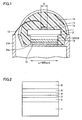
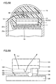
- FIG. 1 is an illustration showing an LED of an Inventive Example A according to a first embodiment of the present invention.
- a laminate construction including a light emitting layer which will be described later, on a first main surface side of a GaN substrate 1 and a p-electrode 12 has been formed thereon.
- This embodiment has a characteristic that this p-electrode 12 is down-mounted to a lead frame mount portion 21a with a conductive adhesive 14.
- a second main surface 1a of GaN substrate 1 is the surface which emits light generated at the light emitting layer and an n-electrode 11 is provided on this surface.
- This n-electrode 11 is formed not to cover the entire surface of the second main surface. It is important to make the ratio of the portion that has not been covered with n-electrode 11 larger. When the opening ratio is made larger, the amount of light shielded by the n-electrode will decrease and therefore the emission efficiency of light emitted outside will be increased.
- N-electrode 11 is electrically connected to a lead portion 21b of a lead frame through a wire 13.
- Wire 13 and the aforementioned laminate construction are sealed with an epoxy resin 15.
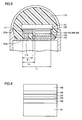
- the laminate construction from GaN substrate 1 to p-electrode 12, of the aforementioned construction, is enlarged in Fig. 2.
- Fig. 2 the laminate construction of Fig. 1 is shown upside down.
- an n-type GaN epitaxial layer 2 is placed on GaN substrate 1 and an n-type Al x Ga 1-X N layer 3 is formed thereon. Further, there is formed thereon a quantum well (MQW) 4 consisting of Al x Ga 1-x N layers and Al x In y Ga 1-x-y N layers.
- a p-type Al x Ga 1-x N layer 5 is placed such that quantum well 4 is sandwiched by p-type Al x Ga 1-x N layer 5 and n-type Al x Ga 1-x N layer 3, and a p-type GaN layer 6 is placed thereon.
- quantum well 4 causes light emission.
- a p-electrode 12 is formed to cover the entire surface of p-type GaN layer 6 and is down-mounted.
- a p-electrode 112 is down-mounted on the lead frame mount portion by conductive adhesive 114. Further, the n electrode is connected to a lead frame mount portion 121a separated from the lead mount portion to which the p-electrode is connected.
- a laminate construction (Fig. 6) including a light emitting layer is formed thereon and is contacted with a predetermined area of n-type GaN layer 102.
- An n-type GaN layer 102 is formed on a sapphire substrate 101 and an n-electrode 111 is formed on the area outside of the area with which the aforementioned laminate construction is contacted.
- the n-electrode 111 is electrically connected to a lead frame mount portion 121a or a lead frame lead portion 121b through a wire or conductive adhesive.
- Light emitted from the light emitting layer is emitted outside through sapphire substrate 101.
- An epoxy resin 115 is encapsulated to cover the aforementioned laminate construction including the sapphire substrate.
- Inventive Example A and Comparative Example B were mounted within an integrating sphere and then predetermined currents were applied to them. The values of output lights which were focused and output from a detector were compared. The result is shown in Fig. 9.
- Fig. 9 under relatively ideal conditions where currents are injected without leaking and there are relatively little non-radiation recombination and low chip-temperature rise due to heat radiation, the light output value increases in proportion to the increase of the applied current. For example, for injection of 20 mA, Inventive Example A generated an output of 8 mW, while Comparative Example B generated an output of 7.2 mW.
- Inventive Example A was mainly constructed by a GaN epitaxial film/GaN substrate, while Comparative Example B was mainly constructed by a GaN epitaxial film/sapphire substrate.
- the sapphire substrate had a refractive index of about 1.8, and this was significantly smaller than the refractive index 2.4 of GaN. Therefore, in Comparative Example B, light was generated in the GaN epitaxial film and propagated, and than the light was prone to total internal reflection at the interface between the GaN epitaxial film and the sapphire substrate. For this reason, the output of Comparative Example B was lower than that of Inventive Example A.
- Inventive Example A unlike in Comparative Example B, the n-electrode and the p-electrode are placed at opposite positions and therefore there is no possibility of electrical short-circuits. Therefore, it is possible to prevent increases of additional fabrication cost such as for providing a film for electrically insulating between the p-electrode and n-electrode for preventing electrical short-circuits in Comparative Example B in which the electrodes exist at the same side.
- test results about the electrostatic withstand voltages of Inventive Example A and Comparative Example B will be described. The tests were performed by generating electric discharge between the light emitting device and an electrostatically charged condenser placed oppositely. At this time, Comparative Example B was broken at an electrostatic voltage of about 100 V. On the other hand, Inventive Example A was not broken until about 8000 V. It was proven that Inventive Example A had an electrostatic withstand voltage which was 80 times that of Comparative Example B.
- the GaN-based light emitting device is formed on the GaN substrate. Therefore, even though the GaN-based light emitting chip is down-mounted so that light is emitted from the back side of the GaN substrate, there is no refractive index difference between them. Thus, light propagates from the GaN-based light emitting chip to the GaN substrate without experiencing total internal reflection. Therefore, as compared with constructions in which a sapphire substrate is employed to form a GaN-based light emitting device, the light output from the GaN substrate main surface may be increased. Further, there will be no extremely-concentrated light emission from the sides of the GaN layer and therefore the sealing resin will not be subjected to damage. Thus, the life time will not be restricted by the sealing resin.
- the inventive example there has been merely described an example of the light emission wavelength 450 nm, and the same effects may be obtained by different light emission wavelengths and layer constructions. Also, it goes without saying that the equivalent effects may be obtained by employing an Al x Ga 1-x N substrate (wherein x is greater than 0 and is equal to or less than 1) instead of the GaN substrate, provided that the substrate has equivalent characteristics.
- Inventive Example C having an increased area will be described.
- Inventive Example C has the same construction as that of Inventive Example A illustrated in Fig. 1.
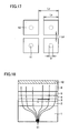
- L1 is 3 mm or tenth and therefore the area is 100 times in Inventive Example C, as illustrated in Fig. 11.
- the fabricating method of Inventive Example C is as follows.
- Figs. 12 and 13 are illustrations showing Inventive Example C 1 which is an modification of Inventive Example C.
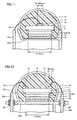
- Inventive Example C 1 is characterized in that n-electrodes 11 are placed at the four corners of the GaN substrate. Further, for mounting the semiconductor chip, a reflective cup 37 is placed in the lead frame such that it surrounds the semiconductor chip.
- Inventive Example C1 In fabricating Inventive Example C1, the same processes as the corresponding processes of Inventive Example A were performed. However, four Au wires were employed as the bonding wires and the diameter of the cross sections of the Au wires was 25 ⁇ m. Each of the electrodes placed at the four corners has a shape of 45 ⁇ m square.
- Comparative Example D has the same construction as that illustrated in Fig. 5. However, L1 was 300 ⁇ m (0.3 mm) in Comparative Example B, L1 is 3 mm and thus tenth in Comparative Example D.
- the size L4 of the portion of the n-type GaN layer for forming an n-electrode is 150 ⁇ m, which is the same as that of Comparative Example B of Fig. 5.
- the fabrication method of Comparative Example D is as follows.
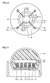
- Comparative Example E is the same as Comparative Examples B and D in that a sapphire substrate is employed and p-electrode 112 and n-electrode 111 are both formed on the down mounting side as illustrated in Fig. 14. Comparative Example E is, however, different from them in that as clearly illustrated in the plan view in Fig. 15, p-electrode 112 has a comb-shape, n-electrodes 111 are placed between the teeth of the comb, and an insulator is placed between p-electrode 112 and n-electrodes 111. This is intended for uniformizing the current flowing through the p-electrode and the n-electrode to prevent formation of areas in which the current density becomes extremely large.
- the fabrication method of this Comparative Example E is as follows.
- n-electrodes 111 five comb electrodes with a width of 0.1 mm was formed with a pitch of 0.5 mm (Figs. 14 and 15).
- the p-electrode was formed at the remaining area of n-type GaN layer 102 such that n-electrodes 111 and p-electrode 112 were spaced by 0.1 mm from each other.
- an insulator 119 for surface protection was formed at the gaps between the n-electrodes and the p-electrode in order to prevent the respective electrodes from being electrically short-circuited.
- a conductive adhesive 114 was provided on the area of mount portion 121a of the lead frame which corresponded to the position of the respective electrodes.
- the chip was mounted to the lead frame while displacement of the chip and the lead frame in the lateral direction, the longitudinal direction and the rotation direction were controlled.
- Inventive Example C and Comparative Example D were mounted within an integrating sphere and then predetermined currents were applied to them. The values of output lights which were focused and output from a detector were compared. For example, when a current of 20 mA was applied, Inventive Example C generated an output of 8 mW, while Comparative Example D generated an output of 7.2 mW. On the other hand, when a current of 2 A (2000 mA) was applied, Inventive Example C generated 100 times the output, namely 800 mW. However, Comparative Example C was broken.
- Comparative Example D under the condition where Comparative Example D was not sealed with resin, electric currents were applied to Comparative Example D and the temperature of the device was measured by a thermoviewer. As a result, it was proven that abnormal heat generation occurred at the area in which currents intensively flowed through the n-type GaN layer in the direction parallel to the layer from the n-electrode toward the MQW light emitting portion and consequently Comparative Example D was broken.
- Comparative Example E generated an output of 7.2 mW for an applied current of 20 mA, and an output of 720 mW for an applied current of 2 A. Thus, Comparative Example E generated outputs which were 0.9 time that of Inventive Example C.
- Inventive Example C1 had an opening ratio much greater than 50% and almost 100%. Further, since n-electrodes are placed at the corners of the GaN substrate, they are much less prone to become obstruction of light emission, as compared with the case where they are placed at the center. As illustrated in Fig. 12, the n electrodes are placed outside of the active layer, in a plan view, the n electrodes will never affect the light emission. As a result, Inventive Example C 1 can achieve higher outputs than Inventive Example C.
- influences of the opening ratio at the light emitting surface and the electrical resistance of the GaN substrate on the light output were determined.
- the adjustment of the opening ratio was performed by varying the substrate area, the p-electrode size and the n-electrode size.
- an LED having the construction illustrated in Fig. 1 was employed.
- some of the tests were performed for a test sample provided with a fluorescence material 26 to be formed as a white LED as illustrated in Fig. 16.
- the test samples were three samples, namely Inventive Example F and Comparative Examples G, H each including a GaN substrate having a resistivity deviated from the range of the present invention.
- an LED including no fluorescence material and sealed with epoxy resin as illustrated in Fig. 1 and a white LED equipped with a fluorescence material illustrated in Fig. 16 were fabricated.
- the opening ratio was defined as follows: ⁇ (area of p-electrode - area of n-electrode/area of p-electrode ⁇ ⁇ 100 (%).
- Inventive Example F and Comparative Examples G and H When applying a current of 20 mA, Inventive Example F and Comparative Examples G and H generated outputs of 8 mW, 7.8 mW and 2.5 mW respectively, which were consistent with the area ratio of the area at which the electrode was not formed. Inventive Example F generated the highest light output. Comparative Example G generated a light output which was not high as that of Inventive Example F, but relatively high. Then, when 500 times the current, or 10 A, was applied to them, Inventive Example F and Comparative Example H generated outputs of 4 mW and 1.3 mW respectively, which were consistent with the area in which the electrode was not formed.
- Comparative Example G increased in proportion to the applied current to 0.1 W at an applied current of 0.26 A and thus at a current density in the light emitting portion of 110 A/cm 2 . However, from then on, the output reached saturation with increasing temperature caused by heat generation and Comparative Example G was broken by an applied current of 10 A.
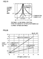
- Figs. 22 and 23 illustrate the results of luminance measurements for the aforementioned three types of test samples.
- Fig. 22 is an illustration showing the relation between the applied current and the resultant luminance for the white-emitting LEDs equipped with a fluorescence material.
- Fig. 23 is similarly an illustration showing the relation between the current and the luminance.
- the same fluorescence material was employed in Inventive Example F and Comparative Example H, but the luminance varied depending on the area ratio of the area at which the electrode was not placed.
- the applied current was 10 A
- the luminances of Inventive Example F and Comparative Example H were 720 1m/chip and 234 lm/chip respectively.
- the Comparative Example had a thermal limit of 18 lm/chip at an applied current of 0.26 A and was broken by an applied current of 10A.
- Figs. 22 and 23 only Inventive Example F generated high luminances at high currents.
- the applied current is 10 mA at a maximum since if the current is increased above that, then the Joule heat density at the n-electrode will become excessive and consequently significant heat generation will occur.
- Inventive Example F-2 an n-electrode with a diameter D of 1 mm (an area of 0.785 mm 2 ) was placed at the center of a GaN substrate.
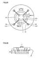
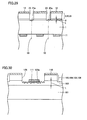
- Inventive Example F-3 n-electrodes of 450 ⁇ m square were placed at the four corners of a GaN substrate (Figs. 24 and 25). As illustrated in Fig. 24 and Fig. 25, the n-electrodes placed at the four corners were each electrically connected to the lead frame by bonding wires.
- the bonding wires were Au wires and had a cross section with a diameter of 300 ⁇ m. In this case, both the examples had an opening ratio of about 100%.
- a reflection cup 37 which was a cup-shaped reflective body was placed.
- Example F the example having no fluorescence material was mounted within an integrating sphere and then predetermined currents were applied to them to cause light emission.
- the value of output light which was focused and output from a detector was measured.
- An output of 8 mW was generated for an applied current of 20 mA, and an output of 4 W was generated for an applied current of 500 times the current or 10 A.
- An output of 28 W was generated for an applied current of 70 A.
- Equivalent outputs can be obtained by placing a plurality of light emitting devices which have small sizes and require relatively low applied currents.
- a constant distance is required between devices, which may significantly increase the entire size or may significantly increase the cost in the case of establishing conduction of each device.
- these problems may be avoided and higher light emission output may be obtained with completely the same number of fabricating process as that of conventional processes, a substantially equivalent cost and a required minimum size.
- the electrodes and the wires will not be obstruction of light emission, and consequently the light output may be further increased.
- a fourth embodiment of the present invention the influence of the GaN substrate thickness on the light output will be described.
- three test samples which are Inventive Examples I, J and K having the same construction as that of the LED illustrated in Fig. 1, the light absorption of the GaN substrates was determined. The fabrication method of the test samples will be described.
- Inventive Example I, J and Comparative Example K having different thicknesses were prepared and the transmittances of the examples for incident light with a wavelength of 380 nm were measured.
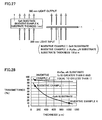
- Figs. 26 and 27 illustrate the general outline of the light transmittance measurement tests.
- Inventive Examples I and J had a thickness of 100 ⁇ m, while Inventive Example K had a greater thickness of 1 mm (1000 ⁇ m).
- Fig. 28 illustrates the test results.
- the transmittances of Inventive Example I and J and Comparative Example K were 70%, 90% and 10%, respectively.
- Inventive Example J three types of substrates having Al atom ratios x of 0.2, 0.5 and 1 were fabricated and all of them had a transmittance of 90%.
- Inventive Examples I, J and Comparative Example K equipped with a fluorescence material to be formed as white LEDs were mounted within an integrating sphere and then predetermined currents were applied to them. The values of output lights which were focused and output from a detector were compared. When a current of 20 mA was applied, Inventive Examples I and J and Comparative Example K generated outputs of 4.2 mW, 5.4 mW (all the aforementioned three types) and 0.6 mA, respectively. This difference was due to the transmittance difference among the substrates. GaN substrates have significantly-low transmittances with respect to lights with wavelengths smaller than 400 nm and in such a case an AlxGa1-xN substrate may be employed as the present invention to generate higher light emission.
- the thickness of the GaN substrate by decreasing the thickness of the GaN substrate, higher light emission may be achieved. If the thickness is too small, the spread range of currents from the n-electrode to the MQW will become too small and if the thickness is too large the emission efficiency will be degraded as previously described. Thus, the thickness is preferably in the range of from 50 ⁇ m to 500 ⁇ m. Further, by using a thin GaN substrate with a thickness of about 100 ⁇ m as the inventive example, the fabrication cost of the GaN substrate may be reduced, which enables fabrication of a low cost light emitting device. It goes without saying that the cost may be reduced by decreasing the substrate thickness independently of the light emission wavelength.
- test samples employed were three samples, which were Inventive Example L having the same construction as that of Inventive Example A employing a GaN substrate and Comparative Examples M, N having the same construction as that of Comparative Example B employing a sapphire substrate.
- the sapphire substrate was an insulator and therefore it was necessary to form the n-electrode on the grown-films side similarly to the p-electrode. Therefore, an attempt was made to expose the n-type GaN layer for forming the n-electrode by etching this wafer from the Mg-doped p-type layers side to the Si-doped n-type GaN layer by photolithography technique and RIE using Cl-based gas.
- the thickness of the Si-doped n-type GaN layer was 100 ⁇ m (0.1 ⁇ m) and thus small, it was impossible to uniformly expose the n-type GaN layer in the wafer. Therefore, there appeared in the exposed surface the n-type Al x Ga 1-x layer or the GaN buffer layer depending on the area. Wet etching using thermal phosphoric acid, etc. was also attempted, any etchants provided the same results.
- Inventive Example L generated an output of 8 mW for an applied current of 20 mA.
- Comparative Example M generated an output of 7.2 mW for the same applied current.
- the n-electrode may be provided on the N-surface of the conductive GaN substrate, and therefore it was unnecessary to expose the Si-doped n-type GaN layer.
- the film thickness of the light emitting device grown on the substrate is, depending on the wavelength or output to be generated, generally 6 ⁇ m or less, and the thickness of the Si-doped n-type GaN layer which occupies most of it may be decreased from 3 ⁇ m to 100 nm according to the inventive example. As a result, with the inventive example, the cost of film growth may be drastically decreased.
- test samples employed were two samples which were Inventive Example O with a dislocation density of 1E6/cm 2 and Comparative Example P with a dislocation density of lE9/cm 2 .
- Inventive Example O and Comparative Example P had the same construction as that of Inventive Example A.
- Inventive Example O and Comparative Example P both generated an output of 8 mW for an applied current of 20 mA and generated outputs of 40 mW and 30 mW respectively for an applied current of 100 mA.
- Inventive Example O may generate a higher light emission output as compared with Comparative Example P.
- Inventive Example O and Comparative Example P had the same resistivity and thickness and therefore cause equivalent heat generation and heat radiation.
- a pulse current with a duty ratio of 1%, an applied time of 1 ⁇ s and a cycle time of 100 ⁇ s was applied and comparison was made. This test results were equivalent to the aforementioned results and thus Inventive Example O and Comparative Example P generated outputs of 40 mW and 30 mW, respectively, for an applied current 100 mA.
- Inventive Example Q was an LED illustrated in Fig. 32 in which the surface and the end face had been non-mirror-surface finished.
- Inventive Example R was an LED illustrated in Fig. 33 which had not been non-mirror-surface finished.
- the light output was determined as the same manner as the first embodiment.
- Inventive Example Q and Comparative Example R respectively, generated outputs of 4. 8 W and 4 W for an applied current of 10 A.
- Inventive Example Q and Comparative Example R were equipped with a fluorescence material to be formed as a white LED, Inventive Example Q generated an output of 1150 lm and Comparative Example R generated an output of 960 lm. Namely, Inventive Example Q generated a higher light emission output. It goes without saying that the same effects may be obtained even when the light emission wavelength is changed. This is because when the surface and the end face of the substrate and the n-type GaN layer are in a mirror-surface state, as illustrated in Fig.
- test samples employed were five samples which were Inventive Examples S, T, U, V and W.
- Inventive Example W was the same as Inventive Example F.
- Inventive Examples S, T, U, V and W generated outputs of 4.8 mW, 4.8 mW, 5.2 mW, 5.8 mW and 4 W for an applied current of 10 A.
- a diagram of reflections at the mounting sides of Inventive Examples S, T is illustrated in Fig. 34
- a diagram of reflections at the mounting side of Inventive Example U is illustrated in Fig. 35
- a diagram of reflections at the mounting side of Inventive Example W is illustrated in Fig. 36.
- a high reflective layer 35 is placed between p-electrode 12 and conductive adhesive 14, while in Inventive Example U, p-electrode 12 itself was a high reflectivity material, and in Inventive Example V, non-mirror-surface finishing had been applied. Further, in Inventive Example W, any consideration was not given to reflections at the mounting side.
- the degree of effects can not be flatly described because when the light emission wavelength is changed the reflectivity of the Ag layer or Al layer and the absorption index of the Ni layer are changed, the effects may be obtained for any wavelength.
- an element with an equivalent or more work function and an equivalent or more reflectivity may be employed to achieve equivalent or more effects.
- the relation between the oxygen concentration and resistivity of the GaN substrate and the light transmittance was grasped. It is characterized in that based on the relation, there was established the relation between optimal GaN substrate thicknesses and oxygen concentrations for predetermined light emission areas, in a light emitting device which was p-down-mounted, namely using a GaN substrate as the light emitting surface. As described above, in the case of p-down-mounting, the light emitting surface is the GaN substrate, and therefore the oxygen concentration which significantly affects the resistivity and the light transmittance is particularly important.
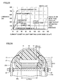
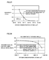
- Fig. 37 is an illustration showing the influence of the oxygen concentration on the resistivity of the GaN substrate. According to Fig. 37, resistivities equal to or lower than 0.5 ⁇ •cm may be realized by setting the oxygen concentration to 1E17/cm 3 or higher.
- Fig. 38 is an illustration showing the influence of the oxygen concentration on the transmittance for light with a wavelength of 450 nm in the case of a -GaN substrate of 400 ⁇ m. From the same figure, it can be seen that when the oxygen concentration exceeds 2E19/cm 3 , the transmittance for light with a wavelength of 450 nm drastically decreases. From Figs.
- increasing the oxygen concentration is effective in decreasing the resistivity of the GaN substrate and widening the light emitting surface, but decreases the light transmittance. Therefore, how to set the oxygen concentration, the GaN substrate thickness and the light emitting plan surface size of a GaN surface used in a light emitting device down-mounted is significantly important.
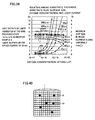
- Fig. 39 is an illustration showing the results of determination of the light outputs and the plan surface sizes of lamps in which currents uniformly flows, wherein the lamps were fabricated from GaN substrates having varying thicknesses and oxygen concentrations in Inventive Example A.
- the larger the thickness and also the higher the oxygen concentration the lower the light output.
- the maximum plan surface size in which current flows uniformly the larger the thickness and also the higher the oxygen concentration, the larger the plan surface size.
- the oxygen concentration may be set to equal to or greater than 6E18/cm 3 for a GaN substrate with a thickness of 200 ⁇ m (equal to or greater than 8E18/cm 3 for a square with a side length of 5 mm) to ensure a light output of 8 mW or more with the size of Inventive Example A and an applied current of 20 mA, and also achieve uniform light emission.
- the current density when the current density is made consistent with the applied current of 20 mA for the size of Inventive Example A having a square shape with a side length of 300 ⁇ m, it corresponds to an applied current of 3.6 A (5.6A) for a square with a side length of 4 mm (a side length of 5mm) and therefore by applying 3.6A (5.6A), a light output of 1.4 W (2.3 W) or more may be ensured in proportion to the applied current and uniform light emission may be achieved.
- the oxygen concentration may be set to 3E18/cm 3 or more for a square with a side length of 4 mm (4E18/cm 3 or more for a square with a side length of 5 mm).
- the oxygen concentration must be set to below 2E19/cm 3 in order to obtain an light output of about 8 mW or more with the size of Inventive Example A when applying 20 mA.
- the limit value of the oxygen concentration which causes the light output to be 8 mW or more for the size of Inventive Example A and the applied current of 20 mA is only slightly higher than 2.5 E18/cm 3 which causes currents to flow uniformly in a square area with a side length of 4 mm. Therefore, there is only narrow oxygen concentration range which satisfies the aforementioned two conditions.
- the oxygen concentration which causes currents to flow uniformly in the square area with a side length of 3 mm is about 2E18/cm 3 and therefore the oxygen concentration permissible range becomes slightly larger as compared with a square with a side length of 4 mm.
- the thickness of the GaN substrate is in the range of 200 ⁇ m to 400 ⁇ m
- there is a sufficiently large oxygen concentration permissible range which enables flowing currents uniformly through a square with a side length of 10 mm and obtaining an output of about 8 mW or more with the size of the Inventive Example A when applying 20 mA.
- this may be enabled by oxygen concentrations equal to or greater than 2E19/cm 3 .
- this may be enabled by oxygen concentrations equal to or greater than 8E18/cm 3 .
- Inventive Example S1 A GaN substrate with a thickness of 400 ⁇ m which had been n-typed with an oxygen concentration of 1E19/cm 3 .
- the resistivity of this GaN substrate was 0.007 ⁇ •cm and the transmittance for light with a wavelength of 450 nm was 72%.
- the portions other than the aforementioned were in the same conditions as that of Inventive Example A. Namely, the plan surface size of the GaN substrate was set such that the light emitting surface had a square shape with a side length of 0.3 mm (see (a1) in the first embodiment).
- (a2) The following laminate construction was formed on the Ga surface, which was a first main surface, of the GaN substrate by MOCVD.
- the light emission intensity was extremely high around the n-electrode and the light emission intensity drastically decreased with increasing distance from the n-electrode. This was because currents flowing thorough the n-electrode did not sufficiently spread within the surface of the light emitting device because of the large resistivity of the GaN substrate. Therefore, light emission occurred only around the p-electrode where currents concentrated. As a result, the light emission output from the entire light emitting device of Comparative Example T2 was lower than that of Inventive Example S1.
- a tenth embodiment of the present invention is characterized in that the density of dislocation bundle in the GaN substrate of a p-down-mounted light emitting device is restricted to increase the light output.
- dislocations which unavoidably generate are concentrated and dislocation bundles are distributed discretely to increase the cystallinity of most areas therebetween in the GaN substrate.
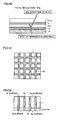
- Dislocation bundles in the GaN substrate as aforementioned are transferred to p-type GaN layer 6 which is an epitaxial film and appear on the epitaxial layer as bundles 61, as illustrated in Fig. 40. Therefore, the dislocation bundles density substantially corresponds to the bundle density.
- These bundles 61 are hole-shaped recesses as illustrated in Fig. 41 depending on the film forming condition of the epitaxial film. The density of hole-shaped recesses drastically affects the fabrication yield, in the case of p-down-mounted light emitting devices including a GaN substrate as the emitting surface.
- test samples were as follows.
- a GaN substrate in which there is a single dislocation bundles per area of 500 ⁇ m ⁇ 500 ⁇ m on average was employed. This corresponds to a dislocation density of 4E2/cm 2 .
- the other conditions are the same as those of Inventive Example S1.
- a GaN substrate in which there is a single dislocation bundle per area of 10 ⁇ m ⁇ 10 ⁇ m on average was employed. This corresponds to a dislocation density of 1E6/cm 2 .
- the other conditions are the same as those of Inventive Example S2.
- a plurality of light emitting devices were constructed from the respective above GaN substrates on an actual production basis.
- a current of 20 mA was applied to the respective test samples and the yield of light emitting devices capable of generating light outputs equal to or higher than 8 mW was determined.
- the yield was 95% in the case of Inventive Example S2 and the yield was 50% in the case of Comparative Example T3.
- the dislocation bundle density is equal to or lower than 4E2/cm 2 , yields which allows actual fabrication may be achieved.
- the dislocation bundle density exceeds the above density, it becomes impossible to actually fabricate light emitting devices continuously on a commercial basis.
- Light emitting devices which were not capable of generating a light output of 8 mW were disassembled and the chip were taken out therefrom and inspected.
- the electrodes were removed from the chips taken out by using a proper acid solution and the chips were inspected from the p-type semiconductor layer side.
- the epitaxial layer was not formed in the area of the GaN substrate where dislocation bundles distributed.
- hole-shaped recesses with diameters of about 1 ⁇ m were observed The above hole-shaped recesses were not found in light emitting devices capable of generating light outputs equal to or higher than 8 mW.
- a current of 20 mA was applied to the aforementioned test samples.
- the driving voltages of the light emitting devices including above hole-shaped recesses were all lower than 1 V. This is because the layers in the p-electrode side and the layers in the n-electrode side were electrically short-circuited since hole-shaped recesses were embedded with the electrode, and as a result currents did not spread through the active layer and sufficient amounts of currents were not supplied, which resulted in lower light output.
- An eleventh embodiment is characterized in that an n-type AlGaN buffer layer and an n-type GaN buffer layer are placed between the GaN substrate and the n-type AIGaN clad layer 3.
- substrates have warpage and GaN substrates have particularly large warpage. Therefore, in a GaN substrate, the off angle significantly varies within the substrate surface, as illustrated in Fig. 42.
- Fig. 42 illustrates an exemplary off-angle distribution with respect to the c-plane of a GaN substrate of 20 mm ⁇ 20 mm.
- the light emitting device formed at the area R1 placed at a corner and having an small off-angle of 0.05° level and the light emitting device formed at the area R2 having a large off-angle of 1.5° level can not generate light outputs of 8 mW or higher for an applied current of 20 mA. This is due to that the crystallinity of the epitaxial film formed on the GaN substrate is not high. Therefore, as illustrated in Fig.
- n-type AlGaN buffer layer 31 having a lattice constant which is middle of those of GaN substrate 1 and AlGaN clad layer 3 between both the layers the difference of lattice constant was alleviated. More specifically, it is characterized in that n-type AlGaN buffer layer 3 is placed at the aforementioned place.
- the off-angle with respect to the c-plane continuously varied from an area with an off-angle of 0.05° to an area with an off-angle of 1.5°.
- This GaN substrate had a resistivity of 0.01 ⁇ •cm, a dislocation density of lE7/cm 2 , and a thickness of 400 ⁇ m.
- light emitting devices were fabricated from respective positions of the above substrate of 20 mm ⁇ 20 mm, according to the fabrication processes (a1) to (a11) of Inventive Example A of the first embodiment.
- an Al 0.15 Ga 0.85 N buffer layer having a thickness of 50 nm was placed between GaN substrate 1 and n-type GaN buffer layer 2.
- a GaN substrate in which in the surface of 20 mm ⁇ 20 mm the off-angle with respect to the c-plane continuously varied from an area with an off-angle of 0.05° to an area with an off-angle of 1.5° was employed.
- This GaN substrate had a resistivity of 0.01 ⁇ •cm, a dislocation density of lE7/cm 2 , and a thickness of 400 ⁇ m.
- a plurality of light emitting devices were fabricated from respective positions, according to the fabrication processes (a1) to (a11) of Inventive Example A of the first embodiment.
- Comparative Example T4 an n-type GaN layer was formed in contact with GaN substrate 1 and an Al 0.15 Ga 0.85 N buffer layer was not placed between the GaN substrate and the n-type GaN buffer layer.
- Inventive Example S3 generated light outputs equal to or higher than 8 mW at the areas of 0.05° to 1.5° including the aforementioned areas R1, R2 (see Fig. 44).
- Comparative Example T4 only the light emitting devices formed at the areas with an off-angles of 0.1° to 1.0° generated light outputs equal to or higher than 8 mW.
- the light outputs were lower than 8 mW.
- an epitaxial layer having an excellent crystallinity may be formed by placing an Al 0.15 Ga 0.85 N buffer layer as described above, according to Inventive Example S3.
- An eleventh embodiment (2) of the present invention is characterized in that by placing an n-type AIGaN buffer layer and an n-type GaN buffer layer between the GaN substrate and n-type AIGaN clad layer 3, hole-shaped recesses illustrated in Fig. 41, which are formed when the epitaxial film is formed on dislocation bundle areas in the GaN substrate as the tenth embodiment, are eliminated.
- a GaN substrate with a diameter of 2 inch in which there is a single dislocation bundle per area of 10 ⁇ m ⁇ 10 ⁇ m was employed, similarly to Comparative Example T3. This corresponds to a dislocation density of 1E6/cm 2 .
- an Al 0.15 Ga 0.85 N buffer layer with a thickness of 50 nm was placed between GaN substrate 1 and n-type buffer layer 2. The other conditions were the same as those of Inventive Example S2.
- the wafer surface at the epitaxial layer side was observed by a differential interference microscope and a SEM (scanning electron microscope). As a result, it was observed that there was no hole-shape recess as illustrated in Fig. 41. An edge of about 5 mm was removed from the perimeter of the GaN substrate with a diameter of 2 inch, and the remaining GaN substrate was all constructed into light emitting devices. Light emitting devices were taken out with a ratio of one out of 50 light emitting devices and a current of 20 mA was applied to the light emitting devices. The yield of light emitting devices capable of generating a light output of equal to or higher than 8 mW was determined. This result was a yield of 100%.
- a twelfth embodiment is characterized in that a p-type AIGaN layer having an increased conductivity is placed outside of MQW4/p-type AIGaN clad layer 5/p-type GaN layer 6 and an Ag electrode layer having a high reflectivity is placed on the entire surface as the p-electrode. Therefore, there is no other metal electrode provided in consideration of work function.
- This construction has a high reflectivity at the down-side bottom, and therefore light absorption which would occur in the case of using other metal electrodes may be reduced and light emission efficiency may be increased.
- test samples were as follows.
- Example A Similarly to Inventive Example A, the following laminate construction was fabricated on the Ga surface, which is a first surface, of a GaN substrate.
- the above laminate construction was characterized in that it had Mg-doped InGaN layer 32 with a thickness of 5 nm in contact with Mg-doped p-type GaN layer 6. Also, while in Inventive Example A according to the first embodiment an Ni/Au electrode layer was formed in process step (a7), the process step of (a7) was not performed and instead of this an Ag electrode layer 33 with a thickness of 100 nm was formed.
- Inventive Example S4 generated an light output of 11.5 mW when a current of 20 mA was applied, while Comparative Example T5 generated 9.6 mW.
- Inventive Example A generated 8 mW.
- Inventive Example S4 generated a higher light output because light traveling from the light emitting layer to the p-semiconductor layers side was reflected at the Ag layer with a reflectivity of 88% since there was no Ni/Au electrode layer and the light was not absorbed at an Ni/Au electrode layer.
- the light output derived to the outside was 1.2 time that of Comparative Example T5.
- any material may be employed as long as the material has a high reflectivity and not-significantly-high contact resistance with p-type InGaN layer 32.
- Al, or Rh may be employed.
- a thirteenth embodiment is characterized in that as the p-electrode Ni/Au layers having a small contact resistance with the p-type GaN layer are discretely placed and an Ag film is applied so as to fill the gaps to increase the light output.
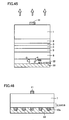
- Fig. 46 is a cross sectional view focused on the p-electrode. Ni/Au electrode layers 12a are placed with a predetermined pitch on the down-side bottom surface of the epitaxial layer. Further, an Ag layer 33 is placed to fill therebetween and cover the down-side bottom surface of the epitaxial layer and Ni/Au electrode layers 12a.
- Fig. 47 is a plan view of the p-electrode viewed through the upper part of the p-electrode.
- the discrete Ni/Au electrode layers 12a generally have a pitch of 3 ⁇ m.
- the pitch of 3 ⁇ m is based on that the diameter of the range of current spread is 6 ⁇ m at best in the typical p-type GaN layer and the p-type AlGaN clad layer due to their resistivities. Namely, by setting the pitch to 3 ⁇ m, currents from a discrete electrode reaches the adjacent electrodes. In order to flow currents through the electrode layer without generating discontinuity, the pitch may be set to below 3 ⁇ m. However, if the pitch is excessively small, the effective amount of extracted light will be decreased by the discretely placed Ni/Au electrode layers.
- Inventive Example S5 was fabricated according to the same fabrication processes as those of Inventive Example A of the first embodiment. However, in the fabrication step (a7) of the p-electrode, an Ni layer with a thickness of 4 nm was formed in contact with the p-type GaN layer and an Au layer with a thickness of 4 nm was formed on the entire surface thereof. Then, patterning was performed using a resist mask to form discretely distributed Ni/Au electrodes (see Figs. 46 and 47). Then, this was heat-treated in the atmosphere of an inert gas to change the contact resistance to 5E-4 ⁇ •cm 2 .
- an Ag layer was formed on the entire surface to fill the gaps of the Ni/Au electrodes and cover the Ni/Au electrodes to form a reflective electrode.
- the area of the discretely-placed Ni/Au layers on the p-type GaN layer was 20% and the area of Ag was 80%. Further, the pitch of Ni/Au electrode layers 12 was 3 ⁇ m (see Fig. 48).
- a laminate construction was formed on a GaN substrate according to the same fabrication processes as those of Inventive Example A of the first embodiment.
- Ni/Au layers were placed on the entire surface in contact with the p-type GaN layer according to the fabrication step (a7) and this was heat-treated.
- an Ag layer was formed on the entire surface in contact with the Ni/Au layer (see Fig. 49).
- a current of 20 mA was applied to the respective light emitting device fabricated as described above and the light outputs were determined.
- Inventive Example S5 generated a light output of 11. 5 mW
- Comparative Example T6 generated a light output of 9.6 mW.
- the ratio of the light which was reflected at the p-electrode and then emitted from the emitting surface, of the light proceeding from the active layer to the mounting side (down side) reached 86% (see Fig. 48).
- the ratio of Comparative Example T6 was 67% (Fig. 49).
- the above ratio of Inventive Example A was 40% (Fig. 50).
- Inventive Example S5 the Ag which occupies 80% of the p-electrode reflects 80% of the light proceeding to the down side with a reflectivity of 88% and the Ni/Au layers which occupy 20% of the p-electrode reflect 20% of the light with a reflectivity higher than 40% (which is not simply a reflectivity of 40%).
- the above ratio of Inventive Example S5 was 86%.
- Comparative Example T6 the light is further reflected by the Ag layer placed at the down side of the Ni/Au layers and therefore the above ratio becomes larger than that of Inventive Example A by the amount of the reflected light.
- Comparative Example T6 belongs to the Inventive Example in the broadest sense. It is defined as a comparative example for convenience in order to explain the present embodiment.
- Ni/Au electrode layers may be substituted with Pt electrode layers or Pd electrode layers.
- the reflective electrode Ag layer may be substituted with a Pt layer or a Rh layer.
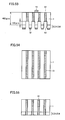
- a fourteenth embodiment of the present invention is characterized in that a plurality of parallel plate-shape crystal inversion domains propagated from the GaN substrate to the epitaxial layer are removed and p-electrodes are placed at the respective gap areas of the plate crystal inversion domains.
- plate-shape crystal inversion domains are distributed in parallel with the thick-wise direction of the GaN substrate and appear in a stripe shape on the main surface of the GaN substrate and the plate crystal inversion domains propagate to the epitaxial layers 2, 3, 4, 5 and 6.
- plate-shape crystal inversion domains are placed in a lattice shape on the main surface.
- the present embodiment is characterized in that crystal inversion domains in the epitaxial layers are completely removed and also crystal inversion domains in the GaN substrate are removed to a predetermined depth in the first main surface side, and then the respective epitaxial layers are isolated and p-electrodes are provided on the respective isolated epitaxial layers (see Fig. 53).
- the plate-shape crystal inversion domains may be lattice-shape inversion domains in which plate-shape crystal inversion domains intersect one another on the main surface or may be parallel arrangement in which plate-shape crystal inversion domains are distributed in alignment in a fixed direction on the main surface, as will be described later.
- the first main surface at the epitaxial layer side has a surface orientation of (0001) surface or c-plane.
- the crystal inversion domains which are symmetric with respect to the first main surface, are (000-1) surface or -c plane and are grown with the c-axis inverted.
- the surface In the c-plane the surface is a Ga surface in which Ga atoms are arranged, while in the crystal inversion domains the surface is an N surface in which N atoms are arranged.
- Inventive Example S6 a GaN substrate in which crystal inversion domains with a width of 30 ⁇ m are arranged with a pitch of 100 ⁇ m in a lattice shape on the first main surface was employed. The crystal inversion domains propagate to the epitaxial films formed on the GaN substrate.
- a laminate construction was formed using the above GaN substrate according to the same fabrication processes as those of Inventive Example A (see steps (a1) to (a6) of Inventive Example A).
- the following process was performed instead of (a7). Namely, by using a mask pattern which covers only the crystal inversion domains propagated to the p-type GaN layer as illustrated in Fig. 52, p-electrode layer was formed on the c-plane areas at the mask gaps, and then the mask pattern was removed.
- the semiconductor substrate was held within 8N (normality)-KOH at 80°C with the entire second main surface (back side) of the above GaN substrate covered with a mask to remove the crystal inversion domains on the first main surface by etching through the epitaxial layers such as the p-type GaN layer to the inside of the GaN substrate and thus slots 52 were formed.
- the plate-shape crystal inversion domains 51 were dislocation-concentrated areas having a high dislocation density and therefore easily etched out by KOH.
- the etching depth into the GaN substrate was to the position at a depth of 150 ⁇ m inside the GaN substrate from the interface between the epitaxial layers and the GaN substrate.
- the mask was removed and an insulator film was deposited so as to fill slots 52 (Fig. 53).
- the above Inventive Example S6 was constructed into a light emitting device and a current of 20 mA was applied.
- the light emitting device generated a light output of 9.6 mW. This light output is 1.2 times the light output of 8 mW of Inventive Example A.
- the plate-shape crystal inversion domains were arranged in a lattice shape, the plate-shape crystal inversion domains are not required to be a lattice shape and may be plate-shape crystal inversion domains arranged only in parallel along a fixed direction on the main surface of the GaN substrate, as illustrated in Fig. 54 (plan view) and Fig. 55 (cross sectional view).
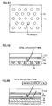
- a fifteenth embodiment of the present invention is characterized in that a fluorescence plate 46 is placed opposite to GaN substrate 1 above the semiconductor chip and the semiconductor chip is sealed with a resin 15.
- a fluorescence plate 46 is placed opposite to GaN substrate 1 above the semiconductor chip and the semiconductor chip is sealed with a resin 15.
- Test samples employed are Inventive Examples S7 and S8 and a Comparative Example T7.
- Inventive Example S7 was basically fabricated according to the fabrication processes of Inventive Example F illustrated in the third embodiment. As illustrated in Fig. 56, above a p-down-mounted chip, a fluorescence plate 46 is placed opposite to the back side of the GaN substrate 1 and the chip was sealed with an epoxy resin 15 to form a white light emission device.
- the above fluorescence plate 46 was fabricated by the following fabrication method.
- this bulk ZnSSe crystal was polished to a thickness of 0.5 mm using a coarse polishing machine and was cut into a shape which could be accommodated in the lead frame.
- Inventive Example S8 projections and depressions were formed on the surface 46a of the above fluorescence plate 46 which faces the GaN substrate (see Fig. 57).
- the height of the projections and depressions was 2 ⁇ m and the average pitch of the projections and depressions was 5 ⁇ m.
- Other structures were the same as those of Inventive Example 57.
- a fluorescence plate 46 was placed opposite to the chip and this chip was sealed with an epoxy resin 15 to form a white light emission device.
- the above GaN substrate has been n-typed by oxygen doping and the oxygen concentration is within the range of oxygen atoms 1E17/cm 3 to 2E19/cm 3 and the thickness of the GaN substrate is from 100 ⁇ m to 600 ⁇ m.
- the resistivity of the GaN substrate may be increased and currents introduced from the p-electrode may be sufficiently spread through the GaN substrate.
- the width of the active layer may be sufficiently utilized to cause light emission.
- the oxygen concentration to 2E19/cm 3 or less, a transmittance equal to or higher than 60% with respect to light with a wavelength of 450 nm may be ensured and thus the transmittance of the GaN substrate which forms the emitting surface may be increased to ensure the light output.
- the above oxygen concentration range effectively works particularly in the case where the thickness of the GaN substrate is from 100 ⁇ m to 600 ⁇ m in a p-down-mounted construction.
- the above oxygen concentration is within the range of oxygen atoms SE18/cm 3 to 2E19/cm 3 and the thickness of the GaN substrate is within the range of from 200 ⁇ m to 400 ⁇ m. Further, the both sides of the rectangular surface which emits light at the second main surface may be equal to or smaller than 10 mm.
- light emission may be caused through the entire light emitting surface and also sufficient light outputs may be obtained.
- the above oxygen concentration may be within the range of oxygen atoms 3E18/cm 3 to 5E18/cm 3 and the thickness of the GaN substrate may be within the range from 400 ⁇ m to 600 ⁇ m. Further, the both sides of the rectangular surface which emits light at the second main surface may be equal to or smaller than 3 mm. Also, the above oxygen concentration may be within the range of oxygen atoms 5E18/cm 3 to 5E19/cm 3 and the thickness of the GaN substrate may be from 100 ⁇ m to 200 ⁇ m. Further, the both sides of the rectangular surface which emits light at the second main surface may be equal to or smaller than 3 mm
- a proper GaN substrate may be set according to the chip size in view of performance (entire surface uniform light emission, light emission efficiency). Further, in view of the fabrication cost, setting of the most desirable conditions may be achieved.
- a GaN substrate in which dislocation bundles are distributed on the first main surface with a density of 4E6/cm 2 or less on average may be employed.
- Dislocation bundles are generated by discretely concentrating dislocations, which have been unavoidably generated during formation of the GaN substrate, in a string shape to distribute them along the substrate thick-wise direction in order to increase the crystalinity of most area of the above GaN substrate.
- light emitting devices having light outputs equal to or higher than a predetermined value may be fabricated with a high fabrication yield.
- the above dislocation bundles may be distributed on the first main surface with a density of 4E2/cm 2 or less on average and the both sides of the rectangular surface which emits light at the second main surface may be within the range of 200 ⁇ m to 400 ⁇ m.
- miniaturized light emitting devices as above include dislocation bundles
- degradation of their characteristics is unavoidable and this will directly lead to reduction of the yield.
- the reduction of the yield may be kept within a practically-accessible range.
- an n-type AIGaN buffer layer may be placed in contact with the GaN substrate and an n-type GaN buffer layer may be placed in contact with the n-type AlGaN buffer layer. Further, an n-type Al x Ga 1-x N layer (0 ⁇ x ⁇ 1) may be placed in contact with the n-type GaN buffer layer.
- an n-type AlGaN buffer layer and an n-type GaN buffer layer may be placed between the GaN substrate and the n-type Al x G 1-x N layer (0 ⁇ x ⁇ 1) which is a clad layer of the active layer.
- n-type AIGaN buffer layer as well as the n-type GaN buffer layer between the above GaN substrate and the clad layer, a hetelo-epitaxial laminate construction with an excellent crystalinity may be formed.
- the above laminate construction may be advantageously employed in the case where the GaN substrate includes areas with an off-angle of 0.10° or less and areas with an off-angle of 1.0° or greater.
- a hetelo-epitaxial laminate construction with an excellent crystalinity may be formed by providing the n-type AIGaN buffer layer as well as the n-type GaN buffer layer between the above GaN substrate and the clad layer.
- Dislocation bundles may be distributed in the above GaN substrate and the dislocation bundles may be made not to be transferred to the epitaxial layers placed on the aforementioned n-type AlGaN buffer layer and the n-type GaN buffer layer placed in contact with the n-type AIGaN buffer layer.
- the fabrication yield may be significantly increased, even when a GaN substrate having a high dislocation bundles density is employed. Namely, by placing the n-type AIGaN buffer layer and the n-type GaN buffer layer as described above, dislocation bundles in the epitaxial laminate construction including the light emitting layer may be substantially removed. Namely, by the above n-type AIGaN buffer layer and the n-type AIGaN buffer layer, dislocation bundles may be terminated at the GaN substrate or near the layer thereon.
- a p-type GaN buffer layer placed at the down side in contact with the above p-type Al x Ga 1-x N layer (0 ⁇ x ⁇ 1) and a p-type InGaN contact layer placed in contact with the p-type GaN buffer layer may be provided.
- the p-type InGaN contact layer with an excellent electrical conductivity may be placed as an underlayer on which the p-electrode is placed.
- the necessity of selecting the material of the p-electrode by placing prime importance on the work function may be reduced. Therefore, the material of the p-electrode may be selected by placing prime importance on the reflectivity, etc.
- the Mg concentration of the aforementioned p-type InGaN contact layer may be within the range of Mg atoms 1E18/cm 3 to 1E21/cm 3 .
- the electrical conductivity may be sufficiently ensured and currents introduced from the p-electrode may be sufficiently spread through the entire epitaxial films.
- a p-electrode layer constituted by an Ag layer may be provided in contact with the above p-type InGaN contact layer.
- the reflectivity at the mounting portion or light emitting device bottom portion may be increased to reduce the light loss, thereby increasing the light output.
- the above GaN substrate includes plate-shape crystal inversion domains extending continuously in the thick-wise direction and within the GaN substrate surface.
- the plate-shape crystal inversion domains in the GaN substrate surface and plate-shape crystal inversion domains propagated to the n-type and p-type nitride semiconductor layers formed on the GaN substrate may be removed from the p-type nitride semiconductor layers side through the n-type nitride semiconductor layers to a position inside of the GaN substrate.
- p-electrodes may be provided on the respective p-type nitride semiconductor layers.
- the light extracting surface may be widened, thereby increasing the light output.
- the plate-shape crystal inversion domains may be removed to a position inside of the GaN substrate by KOH solution.
- a first p-electrode placed discretely over the surface of the p-type nitride semiconductor layer in contact with the p-type nitride semiconductor layer and a second p-electrode formed from Ag which fills the gaps of the first p-electrode and covers the p-type nitride semiconductor layer and the first p-electrode may be provided.
- the coverage ratio of the discretely-placed first p-electrode on the surface of the p-type nitride semiconductor layer may be within the range of 10% to 40%.
- the electrical conductivity may be ensured and introduced currents may be sufficiently spread through the surface.
- the above coverage ratio is lower than 10%, it is impossible to flow currents through the epitaxial layers without generating discontinuity. Also, in the case where the above coverage ratio is higher than 40%, the adverse influence of the discretely-placed p-electrode on the light extraction efficiency becomes significant.
- a fluorescence plate may be placed opposite to the second main surface of the nitride semiconductor substrate apart from the above the nitride semiconductor substrate.
- the fluorescence plate By placing the fluorescence plate directly above the nitride semiconductor substrate constituting the light emitting portion in a p-down-mounted construction, light reflected at the fluorescence plate backside is reflected again at the nitride semiconductor substrate surface and then proceeds toward the fluorescence plate side. As a result, the light output may be increased.
- the surface of the above fluorescence plate which faces the second main surface of the nitride semiconductor substrate may be subjected to a projection/depression forming process.
- the light extraction efficiency may be further increased.
- the above nitride semiconductor substrate may be utilized as a ground member for discharging the electrical power of transient voltages and static discharge to the ground.
- the nitride semiconductor substrate having a high electrical conductivity may be utilized as a ground member for discharging the high voltages to the ground. Consequently, there is no need to provide protection circuits such as electrical power branch circuits including Zener diodes in order to address the above transient voltages and static discharge. Transient voltages and static discharge are main factors of circuit failure for III- nitride semiconductors.
- the nitride semiconductor substrate has a high electrical conductivity as described above, it may be utilized as a ground member to significantly reduce the fabrication processes and the fabrication cost.
- the above light emitting device may cause light emission by applied voltages of equal to or lower than 4 V. Namely, by employing a nitride semiconductor substrate with a high electrical conductivity and therefore low electrical resistance, sufficient currents for light emission may be injected into the light emitting layer by applying low voltages to cause light emission. Consequently, less number of batteries must be mounted and this contributes to reduction of the size, weight and cost of an illumination apparatus equipped with the light emitting device. Further, this is effective in saving electrical power consumption.
- the thickness of the above nitride semiconductor substrate may be 50 ⁇ m or larger.
- the GaN substrate or n-type nitride semiconductor substrate has a large thickness.
- the thickness of the above substrate is smaller than 50 ⁇ m, when the n-electrode area is small, electrons will not sufficiently spread when they reach the active layer of a quantum well construction and accordingly there will be areas generating no light and areas generating insufficient lights in the active layer.
- the thickness of the above substrate By setting the thickness of the above substrate to equal to or greater than 50 ⁇ m, even when the n-electrode area is reduced by the low electrical resistance, currents will sufficiently spread in the substrate and the light emitting area in the active layer may be sufficiently widened. More preferably, the thickness is 75 ⁇ m or greater. However, if the thickness is too large, the absorption at the substrate becomes significant and therefore, it is desirable that the thickness is equal to or smaller than 500 ⁇ m.
- the electrode may be provided on the second main surface of the above nitride semiconductor substrate with an opening ratio of 50% or more.
- the light emission efficiency at the second main surface may be increased.
- the higher the opening ratio the smaller the amount of light absorbed at the n-electrode and thus the larger the light output. Therefore, the opening ratio is preferably 75% or more, and more preferably is 90% or more.
- the contact area between the electrode provided on the above nitride semiconductor substrate and this nitride semiconductor substrate may be 0.055 mm 2 or more.
- a linear current-light output characteristic may be obtained to about 70 A with a 8 mm square-semiconductor chip, without being affected by heat generation at the electrode.
- the cross section area of the bonding wire connecting the above electrode and the lead frame may be 0.002 mm 2 or more.
- the light emitting device may be operated to a current of 2 A without being affected by heat generation at the wire.
- the cross section area of the bonding wire connecting the above electrode and the lead frame may be 0.07 mm 2 or more.
- the light emitting device may be operated to a current of about 70 A without being affected by heat generation at the wire.
- the electrodes may be placed at two or more corners of the nitride semiconductor substrate and the sum of the contact areas between the electrodes and the nitride semiconductor substrate may be 0.055 mm 2 or more. Further, the sum of the cross section areas of the bonding wires connecting the electrodes placed at the corners and the lead frame may be 0.002 mm 2 or more.
- the sum of the cross section areas of the bonding wires connecting the electrodes placed at the corn*ers and the lead frame may be 0.07 mm 2 or more.
- the light emitting area in the above second main surface may be 0.25 mm 2 or more.
- the light emitting area is desired to be larger within the range where currents sufficiently spread in the nitride semiconductor substrate. This means that the lower the electrical resistance the wider the light emitting area may be made.
- the resistivity of the nitride semiconductor substrate is 0.01 ohm-cm
- the light emitting area may be set to about 8 mm ⁇ 8 mm as Inventive Example F.
- the light emitting area of the second main surface of the above nitride semiconductor substrate may be a size equal to or larger than 1 mm ⁇ 1 mm.
- the light emitting area of the second main surface of the above nitride semiconductor substrate may be a size equal to or larger than 3 mm ⁇ 3 mm. Further, The light emitting area of the second main surface of the above nitride semiconductor substrate may be a size equal to or larger than 5 mm ⁇ 5 mm.
- a size equal to or larger than 1 mm ⁇ 1 mm means a size including 1 mm ⁇ 1 mm.
- the above light emitting devices including light emitting devices formed on an AIN substrate, may be formed to have a heat resistance of30°C/W or less.
- the light emission efficiency of a light emitting device is degraded due to temperature increases. Further, if excessive temperature increases are caused, the light emitting device will be damaged. Therefore, the temperature resistance or heat resistance of light emitting devices are an important design factor.
- the heat resistances have been set to about 60°C/W (see the above patent literature 1). However, by setting the heat resistance to 30°C/W or less as previously described, the light emission efficiency will not significantly decrease or the light emitting device will not be damaged even when sufficient electrical power is supplied to the light emitting device.
- the above reduction in the heat resistance to half was realized by using a GnN substrate with a low resistivity as described above.
- the temperature of the portion at which the temperature increases most largely in continuous light emitting conditions may be 150°C or lower.
- the temperature of the portion at which the temperature increases most largely namely the temperature of the light emitting layer, may be 150°C or lower and thus a sufficiently high light emission efficiency may be ensured. Further, the life may be largely extended as compared with conventional light emitting devices.
- the thickness of the n-type nitride semiconductor layer is 3 ⁇ m or less.
- the n-type nitride semiconductor layer is formed on the nitride semiconductor substrate by epitaxial growth. If it is made too thick, it will take longer time to perform film growing processes and also the material cost will be increased. By setting the thickness of the n-type nitride semiconductor layer to 3 ⁇ m or less as previously described, significant cost reduction may be achieved. More preferably, it is 2 ⁇ m or less.
- a non-mirror-surface finishing may be applied to the area of the second main surface of the above nitride semiconductor substrate which is not coated with the electrode.
- the above surface which has been non-mirror surface finished is a surface which has been non-mirror surface finished by using a potassium hydroxide (KOH) solution, sodium hydroxide (NaOH) solution, or ammonia (NH 3 ) solution or other alkali solutions.
- KOH potassium hydroxide
- NaOH sodium hydroxide
- NH 3 ammonia
- the above surface which has been non-mirror surface finished may be a surface which has been non-mirror surface finished by using at least one of sulfuric acid (H 2 SO 4 ) solution, hydrochloric acid (HCI) solution, phosphoric acid (H 2 PO 4 ) solution, hydrofluoric acid (HF) solution or other acid solutions.
- sulfuric acid H 2 SO 4
- hydrochloric acid HAI
- phosphoric acid H 2 PO 4
- HF hydrofluoric acid
- the above surface which has been non-mirror surface finished may be a surface which has been non-mirror surface finished by using RIE
- RIE reactive ion etching
- wet etching using alkali solution in combination with photolithography technique a predetermined projections/depressions pitch may be obtained.
- the electrode formed on the above p-type nitride semiconductor layer may be formed from a material with a reflectivity of 0.5 or more.
- the resistivity is higher and is 0.7 or more.
- a fluorescence member may be placed to cover the second main surface of the above nitride semiconductor substrate.
- the nitride semiconductor substrate may include at least one of impurities or defects which generate fluorescence.
- a white LED may be constructed.
- the light emitting device of the present invention may include two or more above light emitting devices and these light emitting devices may be connected in serial.
- an illumination apparatus including a plurality of the above high efficiency light emitting devices mounted on a lead frame, etc., may be obtained by employing a high voltage power supply.
- batteries for automobile are about 12 V and therefore the light emitting devices of the present invention may be serially connected in four or more stages to cause light emission.
- the light emitting device of the present invention may include two or more above light emitting devices and these light emitting devices may be connected in parallel.
- an illumination apparatus constituted by the above high efficiency light emitting devices may be obtained by employing a high voltage power supply.
- the light emitting device may further include other light emitting devices of the present invention and a power supply circuit for causing the light emitting devices to generate light emission and in the power supply circuit, two or more parallel sections in which two or more light emitting devices are connected in parallel are connected in serial.
- the above power supply circuit may include a parallel/serial switching portion in the case where the capacity of the illumination apparatus is to be variable and the wiring applied to the light emitting devices may be switched by the parallel/serial switching portion.
- the light emitting device of the present invention (1) has a good heat radiation property, does not require a complicated electrode shape, and enables light emission of a high output; (2) has an excellent conductivity, does not require a protection circuit for protecting the light emitting device against transient voltages and static discharge, enables large area light emission, and has a high electrostatic withstand voltage; (3) does not have substantial discontinuity of a refractive index decreasing from a light emitting layer to the substrate, which results in less occurrence of total internal reflection between the light emitting layer and an emitting surface, and therefore avoids decrease in efficiency or degeneration of a resin on a side surface portion due to the total internal reflection; (4) emits light with a low voltage without requiring a large-capacity power supply and is especially suited for an illumination apparatus for an automobile; and (5) can be easily fabricated with a low cost because of its simple construction, and also has high maintainability
Landscapes
- Led Devices (AREA)
- Led Device Packages (AREA)
- Electroluminescent Light Sources (AREA)
Abstract
Description
On the second main surface of the GaN substrate, n-electrodes with a diameter of 100 µm were formed with a pitch of 1.7 mm by photolithography technique, vapor deposition and lift-off method. In this case, the ratio of the area of the second main surface (light emitting surface) of the GaN substrate at which the n-electrode was not formed, namely the opening ratio, was substantially 100% per device. The thickness, the heat treatment and the contact resistance were the same as those of Inventive Example I.
(Process steps to be inserted between q7 and q8) The N-surface of the GaN substrate and the device end face were made to be non-mirror-surfaces. The method for making them to be non-mirror surfaces was performed by dry etching such as RIE or wet etching. Besides this non-mirror-surface finishing method using etching, a method which mechanically polishes may be utilized. In the present embodiment, a method which performs wet etching using a KOH solution as the etchant was employed. A KOH solution of 4 mol/l was sufficiently agitated with the temperature maintained at 40°C and then the wafer was dipped within the stirrer for 30 minutes to non-mirror-surface finish the N-surface of the GaN substrate and the device end face.
Further, of the aforementioned p-electrode, (an Ni layer with a thickness of 4 nm/an Au layer with a thickness of 4 nm) formed in order from the bottom layer in contact with a glass plate was subjected to the same heat treatment and the transmittance was determined. As a result, the transmittance with respect to 450 nm-incident light from the Ni layer side was 70%. Further, an Ag layer with a thickness of 100 nm was formed on a glass plate and the reflectivity was determined. As a result, a reflectivity of 88% was obtained with respect to 450 nm-incident light. Then, (an Ni layer with a thickness of 4 nm/an Au layer with a thickness of 4 nm/an Ag layer with a thickness of 100 nm) was formed on a glass substrate with the Ni layer at the bottom and the same heat treatment was applied. Then, the transmittance was determined.
As a result, a reflectivity of 44% was obtained with respect to 450 nm-incident light. This reflectivity corresponds to the reflectivity when 450 nm-incident light passes through the (Ni layer with a thickness of 4 nm/Au electrode layer with a thickness of 4 nm) with a transmittance of 70%, then is reflected at the Ag layer with a reflectivity of 88% and then passes thorough (the Ni layer with a thickness of 4 nm and the Au electrode layer with a thickness of 4 nm), again, with a transmittance of 70%.
Further, of this electrode, a laminate construction of (an Ni layer with a thickness of 4 nm/an Au layer with a thickness of 4 nm) was formed on a glass plate and the same heat treatment was applied to this construction. Then, the transmittance was determined and as a result the transmittance was 70% with respect to 450 nm-incident light from the Ni layer side. Also, an A1 layer with a thickness of 100 nm was formed on a glass plate and the reflectivity was determined. As a result, the reflectivity was 84% with respect to 450 nm-incident light. Also, a laminate construction of (an Ni layer with a thickness of 4 nm/an Au layer with a thickness of 4 nm/an Al layer with a thickness of 100 nm) was formed in order from the bottom on a glass substrate and the same heat treatment was applied. Then, the transmittance was determined and as a result, a reflectivity of 42% was obtained with respect to 450 nm-incident light. This reflectivity corresponds to the reflectivity calculated for the case where 450 nm-incident light passes through the (Ni layer with a thickness of 4 nm/Au electrode layer with a thickness of 4 nm) with a transmittance of 70%, then is reflected at the Au layer with a reflectivity of 42% and then passes thorough the (Ni layer with a thickness of 4 nm/Au electrode layer with a thickness of 4 nm), again, with a transmittance of 70%.
(Process steps to be inserted between v7 and v8) The same processes as those inserted between q7 and q8 of Inventive Example Q were performed.
Claims (48)
- A light emitting apparatus comprising:a nitride semiconductor substrate (1);a n-type nitride semiconductor layer (3) at a first main surface side of said nitride semiconductor substrate;a p-type nitride semiconductor layer (5), at said first main surface side, placed more distantly from said nitride semiconductor substrate than said n-type nitride semiconductor layer; anda light emitting layer (4), at said first main surface side, placed between said n-type nitride semiconductor layer and said p-type nitride semiconductor layer, whereinsaid nitride semiconductor substrate has a resistivity of 0.5 Ω•cm or less and said p-type nitride semiconductor layer side is down-mounted so that light is emitted from a second main surface of said nitride semiconductor substrate at the opposite side from said first main surface.
- The light emitting apparatus according to claim 1, comprising:a first p-electrode (12a) placed discretely over the surface of said p-type nitride semiconductor layer in contact with said p-type nitride semiconductor layer; anda second p-electrode (33) formed from any one of Ag, Al and Rh which fills the gaps of said first p-electrode and covers said p-type nitride semiconductor layer and said first p-electrode.
- The light emitting apparatus according to claim 2, wherein
the coverage ratio of said first p-electrode on the surface of said p-type nitride semiconductor layer is within the range of 10% to 40%. - The light emitting apparatus according to claim 1, wherein
said light emitting apparatus has an electrostatic withstand voltage of 3000 V or more. - The light emitting apparatus according to claim 1, wherein
there is no protection circuit for protecting said light emitting apparatus against transient voltages or static discharge applied between said nitride semiconductor substrate and said down-mounted p-type AlxGa1-xN layer side. - The light emitting apparatus according to claim 5, wherein
there is no electrical power branch circuit including Zener diodes for addressing said transient voltages or static discharge. - The light emitting apparatus according to claim 1, wherein
said light emitting apparatus causes light emission by an applied voltage of equal to or lower than 4 V. - The light emitting apparatus according to claim 1, wherein
the thickness of said nitride semiconductor substrate is 50 µm or larger. - The light emitting apparatus according to claim 1, wherein
an electrode is provided on the second main surface of said nitride semiconductor substrate with an opening ratio of 50% or more. - The light emitting apparatus according to claim 1, wherein
the contact area between an electrode (11) provided on said nitride semiconductor substrate (1) and said nitride semiconductor substrate is 0.055 mm2 or more. - The light emitting apparatus according to claim 10, wherein
the cross sectional area of a bonding wire (13) connecting said electrode (11) and a lead frame (21b) is 0.002 mm2 or more. - The light emitting apparatus according to claim 11, wherein
the cross sectional area of a bonding wire connecting said electrode and a lead frame is 0.07 mm2 or more. - The light emitting apparatus according to claim 10, wherein
said electrode is placed at two or more corners of said nitride semiconductor substrate and the sum of the contact areas between said electrodes and said nitride semiconductor substrate is 0.055 mm2 or more, and the sum of the cross sectional areas of bonding wires connecting said electrodes placed at said corners and a lead frame is 0.002 mm2 or more. - The light emitting apparatus according to claim 13, wherein
the sum of the cross sectional areas of bonding wires connecting said electrodes placed at said corners and the lead frame is 0.07 mm2 or more. - The light emitting apparatus according to claim 1, wherein
the light emitting area in the second main surface of said nitride semiconductor substrate is 0.25 mm2 or more. - The light emitting apparatus according to claim 1, wherein
the light emitting area of the second main surface of said nitride semiconductor substrate has a size equal to or larger than 1 mm × 1 mm. - The light emitting apparatus according to claim 16, wherein
the light emitting area of the second main surface of said nitride semiconductor substrate has a size equal to or larger than 3 mm × 3 mm. - The light emitting apparatus according to claim 16, wherein
the light emitting area of the second main surface of said nitride semiconductor substrate has a size equal to or larger than 5 mm × 5 mm. - The light emitting apparatus according to claim 1, which is constituted to have a heat resistance of 30°C/W or less.
- The light emitting apparatus according to claim 1, wherein
the temperature of the portion at which the temperature increases most largely in continuous light emitting conditions is 150°C or lower. - The light emitting apparatus according to claim 1, wherein
the thickness of said n-type nitride semiconductor layer is 3 µm or less. - The light emitting apparatus according to claim 1, wherein
the area of the second main surface of said nitride semiconductor substrate which is not coated with said electrode has been non-mirror-surface finished. - The light emitting apparatus according to claim 22, wherein
said surface which has been non-mirror-surface finished is a surface which has been non-mirror-surface finished by using potassium hydroxide (KOH) solution, sodium hydroxide (NaOH) solution, or ammonia (NH3) solution or other alkali solutions. - The light emitting apparatus according to claim 22, wherein
said surface which has been non-mirror-surface finished is a surface which has been non-mirror-surface finished by using at least one of sulfuric acid (H2SO4) solution, hydrochloric acid (HCl) solution, phosphoric acid (H2PO4) solution, hydrofluoric acid (HF) solution or other acid solutions. - The light emitting apparatus according to claim 22, wherein
said surface which has been non-mirror-surface finished is a surface which has been non-mirror-surface finished by using reactive ion etching (RIE). - The light emitting apparatus according to claim 1, wherein
said electrode (12) provided on said p-type nitride semiconductor layer is formed from a material with a reflectivity of 0.5 or more. - The light emitting apparatus according to claim 1, wherein
a fluorescence member (26) is placed to cover the second main surface of said nitride semiconductor substrate. - The light emitting apparatus according to claim 1, wherein
a fluorescence plate (46) is placed opposite to the second main surface of said nitride semiconductor substrate apart from said nitride semiconductor substrate. - The light emitting apparatus according to claim 28, wherein
the surface of said fluorescence plate which faces the second main surface of said nitride semiconductor substrate has been subjected to a projection/depression forming process. - The light emitting apparatus according to claim 1, wherein
said nitride semiconductor substrate include at least one of impurities and defects which generate fluorescence. - A light emitting apparatus comprising:two or more light emitting apparatuses according to claim 1 and these light emitting apparatuses are connected in serial or parallel.
- The light emitting apparatus comprising said light emitting apparatuses according to claim 1 and a power supply circuit for causing the light emitting apparatuses to generate light emission, wherein in said power supply circuit, two or more parallel sections in which two or more said light emitting apparatuses are connected in parallel are connected in serial.
- A light emitting apparatus comprising:a GaN substrate (1) which is a nitride semiconductor substrate;an n-type AlxGa1-xN layer (x is in the range of from 0 to 1) (3) which is an n-type nitride semiconductor layer at a first main surface side of said GaN substrate;a p-type AlxGa1-xN layer (x is within the range of from 0 to 1) (5), at said first main surface side, placed more distantly from said GaN substrate than said n-type AlxGa1-xN layer; anda light emitting layer (4), at said first main surface side, placed between said n-type AlxGa1-xN layer and said p-type AlxGa1-xN layer, whereinsaid GaN substrate has a dislocation density of 108/cm2 or less, and said p-type AlxGa1-xN layer side is down-mounted so that light is emitted from the second main surface of said GaN substrate at the opposite side from the first main surface.
- The light emitting apparatus according to claim 33, wherein
said GaN substrate has been n-typed by oxygen doping, the oxygen concentration is within the range of oxygen atoms 1E17/cm3 to 2E 19/cm3 and the thickness of said GaN substrate is from 100 µm to 600 µm. - The light emitting apparatus according to claim 33, wherein
said oxygen concentration is within the range of oxygen atoms 5E18/cm3 to 2E19/cm3 and the thickness of said GaN substrate is within the range of from 200 µm to 400 µm and the both sides of the rectangular surface which emits light at said main surface is equal to or smaller than 10 mm. - The light emitting apparatus according to claim 33, wherein
said oxygen concentration is within the range of oxygen atoms 3E18/cm3 to 5E18/cm3 and the thickness of said GaN substrate is within the range of from 400 µm to 600 µm and the both sides of the rectangular surface which emits light at said second main surface is equal to or smaller than 3 mm. - The light emitting apparatus according to claim 33, wherein
said oxygen concentration is within the range of oxygen atoms 5E18/cm3 to 5E19/cm3 and the thickness of said GaN substrate is within the range of from 100 µm to 200 µm and the both sides of the rectangular surface which emits light at said second main surface is equal to or smaller than 3 mm. - The light emitting apparatus according to claim 33, wherein
dislocation bundles (61) are distributed on the first main surface of said GaN substrate with a density of 4E6/cm2 or less on average and said dislocation bundles are generated by discretely concentrating dislocations, which have been unavoidably generated during formation of the GaN substrate, in a string shape to distribute them along the substrate thick-wise direction in order to increase the crystalinity of most area of said GaN substrate. - The light emitting apparatus according to claim 33, wherein
said dislocation bundles are distributed on said first main surface with a density of 4E2/cm2 or less on average and the both sides of the rectangular surface which emits light at said second main surface is within the range of 200 µm to 400 µm. - The light emitting apparatus according to claim 33, wherein
between said GaN substrate and said n-type AlxGa1-xN layer (x is within the range of from 0 to 1), an n-type AlGaN buffer layer (31) is placed in contact with said GaN substrate and an n-type GaN buffer layer (2) is placed in contact with the n-type AIGaN buffer layer, and said n-type AlxGa1-xN layer (x is within the range of from 0 to 1) (3) is placed in contact with the n-type GaN buffer layer. - The light emitting apparatus according to claim 40, wherein
said GaN substrate includes areas with an off-angle of 0.10° or less and areas with an off-angle of 1.0° or greater. - The light emitting apparatus according to claim 40, wherein
dislocation bundles (61) are distributed in said GaN substrate and said dislocation bundles are not transferred to said n-type AlxGa1-xN layer (x is within the range of 0 to 1) (3) placed in contact with said GaN buffer layer. - The light emitting apparatus according to claim 33 comprising a p-type
GaN buffer layer (6) placed at the down side in contact with said p-type AlxGa1-xN layer (x is within the range of from 0 to 1) (5) and a p-type InGaN contact layer (32) placed in contact with the p-type GaN buffer layer. - The light emitting apparatus according to claim 43, wherein
the Mg concentration of said p-type InGaN contact layer (32) is within the range of Mg atoms 1E18/cm3 to 1E21/cm3. - The light emitting apparatus according to claim 43 comprising a p-electrode layer (33) formed from any one of Ag, Al and Rh in contact with said p-type InGaN contact layer (32).
- The light emitting apparatus according to claim 33, wherein
said GaN substrate includes plate-shape crystal inversion domains (51) extending continuously in a plane shape in the thick-wise direction and a single direction within the GaN substrate surface, the plate-shape crystal inversion domains within the GaN substrate surface and plate-shape crystal inversion domains propagated to said n-type and p-type nitride semiconductor layers formed on said GaN substrate are removed from said p-type nitride semiconductor layers side through said n-type nitride semiconductor layers to a position inside of said GaN substrate, and in contact with the left p-type nitride semiconductor layers, p-electrodes (12) are provided on the respective p-type nitride semiconductor layers. - The light emitting apparatus according to claim 46, wherein
said plate-shape crystal inversion domains are removed to a position inside of said GaN substrate by KOH solution. - A light emitting apparatus comprising:a conductive A1N substrate which is a nitride semiconductor substrate;an n-type AlxGa1-xN layer (x is in the range of from 0 to 1) which is an n-type nitride semiconductor layer at a first main surface side of said AlN substrate;a p-type AlxGa1-xN layer (x is in the range of from 0 to 1), at said first main surface side, placed more distantly from said AIN substrate than said n-type AlxGa1-xN layer; anda light emitting layer, at said first main surface side, placed between said n-type AlxGa1-xN layer and said p-type AlxGa1-xN layer, whereinsaid AIN substrate has a heat conductivity of 100 W/(m•K) or higher, and said p-type AlxGa1-xN layer side is down-mounted so that light is emitted from a second main surface of said AIN substrate at the opposite side from said first main surface.
Applications Claiming Priority (5)
| Application Number | Priority Date | Filing Date | Title |
|---|---|---|---|
| JP2003301706 | 2003-08-26 | ||
| JP2003301706 | 2003-08-26 | ||
| JP2003429818 | 2003-12-25 | ||
| JP2003429818 | 2003-12-25 | ||
| PCT/JP2004/011158 WO2005020337A1 (en) | 2003-08-26 | 2004-08-04 | Light-emitting device |
Publications (2)
| Publication Number | Publication Date |
|---|---|
| EP1571716A1 true EP1571716A1 (en) | 2005-09-07 |
| EP1571716A4 EP1571716A4 (en) | 2012-07-25 |
Family
ID=34220742
Family Applications (1)
| Application Number | Title | Priority Date | Filing Date |
|---|---|---|---|
| EP04771196A Withdrawn EP1571716A4 (en) | 2003-08-26 | 2004-08-04 | PHOTO-EMITTING DEVICE |
Country Status (9)
| Country | Link |
|---|---|
| US (2) | US7202509B2 (en) |
| EP (1) | EP1571716A4 (en) |
| JP (2) | JP3841092B2 (en) |
| KR (1) | KR100919657B1 (en) |
| CN (1) | CN100414724C (en) |
| CA (1) | CA2509785A1 (en) |
| SG (1) | SG145722A1 (en) |
| TW (1) | TW200522392A (en) |
| WO (1) | WO2005020337A1 (en) |
Cited By (3)
| Publication number | Priority date | Publication date | Assignee | Title |
|---|---|---|---|---|
| EP1670074A3 (en) * | 2004-12-08 | 2010-11-17 | Sumitomo Electric Industries, Ltd. | Light emitting diode headlamp |
| EP1672704A3 (en) * | 2004-12-20 | 2010-11-17 | Sumitomo Electric Industries, Ltd. | Light emitting device |
| WO2020106914A1 (en) * | 2018-11-21 | 2020-05-28 | Analog Devices, Inc. | Superlattice photodetector/light emitting diode |
Families Citing this family (44)
| Publication number | Priority date | Publication date | Assignee | Title |
|---|---|---|---|---|
| JP3841092B2 (en) | 2003-08-26 | 2006-11-01 | 住友電気工業株式会社 | Light emitting device |
| JP2005191530A (en) | 2003-12-03 | 2005-07-14 | Sumitomo Electric Ind Ltd | Light emitting device |
| CN101061590B (en) * | 2004-11-18 | 2010-05-12 | 皇家飞利浦电子股份有限公司 | Light emitter and its manufacturing method |
| JP4244953B2 (en) * | 2005-04-26 | 2009-03-25 | 住友電気工業株式会社 | Light emitting device and manufacturing method thereof |
| JP2006324324A (en) * | 2005-05-17 | 2006-11-30 | Sumitomo Electric Ind Ltd | Light emitting device, method for manufacturing light emitting device, and nitride semiconductor substrate |
| JP4297084B2 (en) * | 2005-06-13 | 2009-07-15 | 住友電気工業株式会社 | LIGHT EMITTING DEVICE MANUFACTURING METHOD AND LIGHT EMITTING DEVICE |
| US20060289891A1 (en) * | 2005-06-28 | 2006-12-28 | Hutchins Edward L | Electronic and/or optoelectronic devices grown on free-standing GaN substrates with GaN spacer structures |
| CN100565948C (en) * | 2005-06-30 | 2009-12-02 | 松下电工株式会社 | Light-emitting device |
| JP2007019099A (en) * | 2005-07-05 | 2007-01-25 | Sumitomo Electric Ind Ltd | Light emitting device and manufacturing method thereof |
| JP2007088420A (en) * | 2005-08-25 | 2007-04-05 | Sharp Corp | Manufacturing method of semiconductor light emitting device |
| JP2007088389A (en) * | 2005-09-26 | 2007-04-05 | Yamaguchi Univ | Apparatus and method for measuring internal quantum efficiency of semiconductor light emitting device |
| US7928462B2 (en) | 2006-02-16 | 2011-04-19 | Lg Electronics Inc. | Light emitting device having vertical structure, package thereof and method for manufacturing the same |
| JP2007266574A (en) * | 2006-02-28 | 2007-10-11 | Sanyo Electric Co Ltd | Semiconductor laser element, and manufacturing method of semiconductor laser element |
| US7754514B2 (en) | 2006-08-22 | 2010-07-13 | Toyoda Gosei Co., Ltd. | Method of making a light emitting element |
| JP4894411B2 (en) * | 2006-08-23 | 2012-03-14 | 日立電線株式会社 | Semiconductor light emitting device |
| JP2008140893A (en) * | 2006-11-30 | 2008-06-19 | Sumitomo Electric Ind Ltd | Semiconductor device and manufacturing method thereof |
| US8080833B2 (en) * | 2007-01-26 | 2011-12-20 | Crystal Is, Inc. | Thick pseudomorphic nitride epitaxial layers |
| JP5133087B2 (en) * | 2007-02-23 | 2013-01-30 | 株式会社ニューフレアテクノロジー | Manufacturing method of semiconductor device |
| TWI331816B (en) * | 2007-04-03 | 2010-10-11 | Advanced Optoelectronic Tech | Semiconductor light-emitting device |
| US8104945B2 (en) * | 2007-12-27 | 2012-01-31 | Samsung Led Co., Ltd. | Backlight unit implementing local dimming for liquid crystal display device |
| JP4692602B2 (en) | 2008-09-26 | 2011-06-01 | 住友電気工業株式会社 | Gallium nitride based epitaxial wafer and method for producing epitaxial wafer |
| JP5211996B2 (en) * | 2008-09-30 | 2013-06-12 | 豊田合成株式会社 | Light emitting device |
| US20110024775A1 (en) * | 2009-07-31 | 2011-02-03 | Goldeneye, Inc. | Methods for and devices made using multiple stage growths |
| JPWO2011016201A1 (en) * | 2009-08-06 | 2013-01-10 | パナソニック株式会社 | Light emitting element and light emitting device |
| KR101081166B1 (en) * | 2009-09-23 | 2011-11-07 | 엘지이노텍 주식회사 | Light emitting device, method for fabricating the same and light emitting device package |
| JP5381581B2 (en) * | 2009-09-30 | 2014-01-08 | 住友電気工業株式会社 | Gallium nitride substrate |
| KR101034054B1 (en) * | 2009-10-22 | 2011-05-12 | 엘지이노텍 주식회사 | Light emitting device package and manufacturing method thereof |
| TWI412161B (en) * | 2009-11-06 | 2013-10-11 | Semileds Optoelectronics Co | Light-emitting diode device |
| KR101103892B1 (en) * | 2009-12-08 | 2012-01-12 | 엘지이노텍 주식회사 | Light emitting device and light emitting device package |
| JP4913927B1 (en) * | 2010-09-01 | 2012-04-11 | 昭和電工株式会社 | ELECTROLUMINESCENT ELEMENT, DISPLAY DEVICE AND LIGHTING DEVICE |
| WO2012147390A1 (en) * | 2011-04-28 | 2012-11-01 | 昭和電工株式会社 | Organic light-emitting element, production method for organic light-emitting element, display device, and illumination device |
| KR20140001249A (en) * | 2011-05-19 | 2014-01-06 | 쇼와 덴코 가부시키가이샤 | Organic light-emitting element, method for making organic light-emitting element, display device and illumination device |
| EP2752894A3 (en) * | 2011-08-09 | 2014-10-22 | Panasonic Corporation | Semiconductor light-emitting device and light source device including the same |
| US9184346B2 (en) | 2011-12-12 | 2015-11-10 | Sensor Electronic Technology, Inc. | Ultraviolet reflective contact |
| US9818912B2 (en) | 2011-12-12 | 2017-11-14 | Sensor Electronic Technology, Inc. | Ultraviolet reflective contact |
| WO2013124924A1 (en) | 2012-02-23 | 2013-08-29 | パナソニック株式会社 | Nitride semiconductor light-emitting chip, nitride semiconductor light-emitting device, and method for manufacturing nitride semiconductor chip |
| US20150102307A1 (en) * | 2012-02-29 | 2015-04-16 | Showa Denko K.K. | Electroluminescent element, method for manufacturing electroluminescent element, display device, and illumination device |
| US10020431B2 (en) * | 2012-03-30 | 2018-07-10 | Lumileds Llc | Sealed semiconductor light emitting device |
| CN103511995B (en) * | 2012-06-29 | 2016-04-20 | 展晶科技(深圳)有限公司 | Light-emitting diode light bar |
| KR102076235B1 (en) * | 2012-08-29 | 2020-02-12 | 엘지이노텍 주식회사 | Backlight unit |
| KR102335452B1 (en) * | 2015-06-16 | 2021-12-07 | 서울바이오시스 주식회사 | Light emitting device |
| KR102487989B1 (en) * | 2015-09-30 | 2023-01-12 | 쑤저우 레킨 세미컨덕터 컴퍼니 리미티드 | Light emitting device |
| US10665753B2 (en) | 2016-03-01 | 2020-05-26 | Stanley Electric Co., Ltd. | Vertical-type ultraviolet light-emitting diode |
| JP2021012900A (en) * | 2019-07-03 | 2021-02-04 | パナソニックIpマネジメント株式会社 | Group III nitride semiconductor laser device |
Family Cites Families (68)
| Publication number | Priority date | Publication date | Assignee | Title |
|---|---|---|---|---|
| JPS5455390A (en) | 1977-10-12 | 1979-05-02 | Nec Corp | Light emitting element |
| JP2685377B2 (en) * | 1990-11-26 | 1997-12-03 | シャープ株式会社 | Compound semiconductor light emitting device |
| JPH05251739A (en) * | 1992-03-06 | 1993-09-28 | Toshiba Corp | Semiconductor light emitting device |
| JP2836687B2 (en) | 1993-04-03 | 1998-12-14 | 日亜化学工業株式会社 | Gallium nitride based compound semiconductor light emitting device |
| TW290743B (en) | 1995-03-27 | 1996-11-11 | Sumitomo Electric Industries | |
| JPH08279627A (en) | 1995-04-07 | 1996-10-22 | Showa Denko Kk | Light emitting element |
| US6783867B2 (en) | 1996-02-05 | 2004-08-31 | Sumitomo Electric Industries, Ltd. | Member for semiconductor device using an aluminum nitride substrate material, and method of manufacturing the same |
| JP3644191B2 (en) | 1996-06-25 | 2005-04-27 | 住友電気工業株式会社 | Semiconductor element |
| JP3087829B2 (en) | 1996-10-14 | 2000-09-11 | 日亜化学工業株式会社 | Method for manufacturing nitride semiconductor device |
| JP3772801B2 (en) | 1996-11-05 | 2006-05-10 | 日亜化学工業株式会社 | Light emitting diode |
| JP3409666B2 (en) | 1996-12-02 | 2003-05-26 | 日亜化学工業株式会社 | Surface light emitting device and display device using the same |
| JP3787220B2 (en) | 1997-07-30 | 2006-06-21 | ローム株式会社 | Chip light emitting device |
| JP3551751B2 (en) | 1997-05-16 | 2004-08-11 | 日亜化学工業株式会社 | Method for growing nitride semiconductor |
| JP2868085B2 (en) | 1997-05-20 | 1999-03-10 | 日亜化学工業株式会社 | Planar light source |
| JPH1097200A (en) | 1997-05-20 | 1998-04-14 | Nichia Chem Ind Ltd | Light source |
| JP3898798B2 (en) | 1997-05-27 | 2007-03-28 | シャープ株式会社 | Method for manufacturing gallium nitride compound semiconductor light emitting device |
| JP3457516B2 (en) | 1997-08-27 | 2003-10-20 | 株式会社東芝 | Gallium nitride based compound semiconductor device |
| JP3618989B2 (en) | 1997-12-24 | 2005-02-09 | 株式会社東芝 | Semiconductor laser device |
| US6841800B2 (en) * | 1997-12-26 | 2005-01-11 | Matsushita Electric Industrial Co., Ltd. | Light-emitting device comprising a gallium-nitride-group compound-semiconductor |
| JPH11220176A (en) | 1998-02-03 | 1999-08-10 | Matsushita Electron Corp | Semiconductor light emitting device |
| JP4169821B2 (en) | 1998-02-18 | 2008-10-22 | シャープ株式会社 | Light emitting diode |
| JP3707279B2 (en) * | 1998-03-02 | 2005-10-19 | 松下電器産業株式会社 | Semiconductor light emitting device |
| TW428331B (en) | 1998-05-28 | 2001-04-01 | Sumitomo Electric Industries | Gallium nitride single crystal substrate and method of producing the same |
| JP3788104B2 (en) | 1998-05-28 | 2006-06-21 | 住友電気工業株式会社 | Gallium nitride single crystal substrate and manufacturing method thereof |
| JP3788037B2 (en) | 1998-06-18 | 2006-06-21 | 住友電気工業株式会社 | GaN single crystal substrate |
| TW406442B (en) * | 1998-07-09 | 2000-09-21 | Sumitomo Electric Industries | White colored LED and intermediate colored LED |
| JP3966623B2 (en) | 1998-07-14 | 2007-08-29 | 富士フイルム株式会社 | Process for producing N-alkyl-α-dialkylaminoacetohydroxamic acid compounds |
| JP3397141B2 (en) | 1998-07-28 | 2003-04-14 | 住友電気工業株式会社 | White LED |
| TW413956B (en) | 1998-07-28 | 2000-12-01 | Sumitomo Electric Industries | Fluorescent substrate LED |
| JP2000077713A (en) | 1998-08-27 | 2000-03-14 | Sanyo Electric Co Ltd | Semiconductor light emitting device |
| JP2000223751A (en) | 1998-11-25 | 2000-08-11 | Nichia Chem Ind Ltd | Led lamp and display device using the led lamp |
| JP4296644B2 (en) | 1999-01-29 | 2009-07-15 | 豊田合成株式会社 | Light emitting diode |
| JP3668031B2 (en) | 1999-01-29 | 2005-07-06 | 三洋電機株式会社 | Method for manufacturing nitride-based semiconductor light-emitting device |
| JP4136272B2 (en) * | 1999-08-30 | 2008-08-20 | 株式会社リコー | Semiconductor light emitting device |
| US6614821B1 (en) * | 1999-08-04 | 2003-09-02 | Ricoh Company, Ltd. | Laser diode and semiconductor light-emitting device producing visible-wavelength radiation |
| JP4005275B2 (en) | 1999-08-19 | 2007-11-07 | 日亜化学工業株式会社 | Nitride semiconductor device |
| US6885035B2 (en) | 1999-12-22 | 2005-04-26 | Lumileds Lighting U.S., Llc | Multi-chip semiconductor LED assembly |
| US6514782B1 (en) | 1999-12-22 | 2003-02-04 | Lumileds Lighting, U.S., Llc | Method of making a III-nitride light-emitting device with increased light generating capability |
| US6447604B1 (en) * | 2000-03-13 | 2002-09-10 | Advanced Technology Materials, Inc. | Method for achieving improved epitaxy quality (surface texture and defect density) on free-standing (aluminum, indium, gallium) nitride ((al,in,ga)n) substrates for opto-electronic and electronic devices |
| JP2001326425A (en) | 2000-05-12 | 2001-11-22 | Fuji Photo Film Co Ltd | Method of manufacturing substrate for semiconductor element and semiconductor element |
| JP2002016311A (en) | 2000-06-27 | 2002-01-18 | Sharp Corp | Gallium nitride based light emitting device |
| JP3834188B2 (en) | 2000-07-10 | 2006-10-18 | 日亜化学工業株式会社 | Semiconductor light emitting device |
| EP1320884A2 (en) | 2000-09-11 | 2003-06-25 | Tokyo Electron Limited | Semiconductor device and fabrication method therefor |
| JP4430264B2 (en) | 2001-03-19 | 2010-03-10 | 日亜化学工業株式会社 | Surface mount light emitting device |
| US6806508B2 (en) * | 2001-04-20 | 2004-10-19 | General Electic Company | Homoepitaxial gallium nitride based photodetector and method of producing |
| JP2002319705A (en) * | 2001-04-23 | 2002-10-31 | Matsushita Electric Works Ltd | LED device |
| CN1259734C (en) * | 2001-06-13 | 2006-06-14 | 松下电器产业株式会社 | Nitride semiconductor, manufacturing method thereof, and nitride semiconductor device |
| JP4122739B2 (en) | 2001-07-26 | 2008-07-23 | 松下電工株式会社 | Light emitting device and manufacturing method thereof |
| CN1215574C (en) | 2001-08-08 | 2005-08-17 | 洲磊科技股份有限公司 | Light-emitting diode with distributed current and improved light-emitting area utilization |
| JP4244542B2 (en) | 2001-08-28 | 2009-03-25 | 日亜化学工業株式会社 | Gallium nitride compound semiconductor light emitting device and method for manufacturing the same |
| JP2003086843A (en) | 2001-09-14 | 2003-03-20 | Sharp Corp | Semiconductor light emitting element and semiconductor light emitting device |
| JP3801125B2 (en) | 2001-10-09 | 2006-07-26 | 住友電気工業株式会社 | Single crystal gallium nitride substrate, method for crystal growth of single crystal gallium nitride, and method for manufacturing single crystal gallium nitride substrate |
| JP3864870B2 (en) | 2001-09-19 | 2007-01-10 | 住友電気工業株式会社 | Single crystal gallium nitride substrate, growth method thereof, and manufacturing method thereof |
| JP3920613B2 (en) | 2001-10-02 | 2007-05-30 | 三洋電機株式会社 | Optical semiconductor device |
| US6744072B2 (en) | 2001-10-02 | 2004-06-01 | Xerox Corporation | Substrates having increased thermal conductivity for semiconductor structures |
| JP4920152B2 (en) | 2001-10-12 | 2012-04-18 | 住友電気工業株式会社 | Structure substrate manufacturing method and semiconductor device manufacturing method |
| WO2003035945A2 (en) | 2001-10-26 | 2003-05-01 | Ammono Sp. Zo.O. | Substrate for epitaxy |
| JP4383172B2 (en) * | 2001-10-26 | 2009-12-16 | アンモノ・スプウカ・ジ・オグラニチョノン・オドポヴィエドニアウノシツィオン | Light emitting device structure using nitride bulk single crystal layer and manufacturing method thereof |
| JP2003218401A (en) | 2002-01-18 | 2003-07-31 | Matsushita Electric Ind Co Ltd | Semiconductor light emitting device and method of manufacturing the same |
| US6984460B2 (en) | 2002-03-26 | 2006-01-10 | Tdk Corporation | Phosphor thin film, manufacturing method of the same, and electroluminescence panel |
| US6791120B2 (en) | 2002-03-26 | 2004-09-14 | Sanyo Electric Co., Ltd. | Nitride-based semiconductor device and method of fabricating the same |
| JP2003326425A (en) | 2002-05-10 | 2003-11-18 | Toyota Motor Corp | Nutrunner |
| EP1394857A3 (en) * | 2002-08-28 | 2004-04-07 | Matsushita Electric Industrial Co., Ltd. | Semiconductor device |
| US7112830B2 (en) * | 2002-11-25 | 2006-09-26 | Apa Enterprises, Inc. | Super lattice modification of overlying transistor |
| JP3841092B2 (en) | 2003-08-26 | 2006-11-01 | 住友電気工業株式会社 | Light emitting device |
| US7009215B2 (en) | 2003-10-24 | 2006-03-07 | General Electric Company | Group III-nitride based resonant cavity light emitting devices fabricated on single crystal gallium nitride substrates |
| JP2005191530A (en) * | 2003-12-03 | 2005-07-14 | Sumitomo Electric Ind Ltd | Light emitting device |
| JP2006179511A (en) | 2004-12-20 | 2006-07-06 | Sumitomo Electric Ind Ltd | Light emitting device |
-
2004
- 2004-07-13 JP JP2004206269A patent/JP3841092B2/en not_active Expired - Fee Related
- 2004-08-04 CA CA002509785A patent/CA2509785A1/en not_active Abandoned
- 2004-08-04 CN CNB2004800098998A patent/CN100414724C/en not_active Expired - Fee Related
- 2004-08-04 SG SG200805892-7A patent/SG145722A1/en unknown
- 2004-08-04 EP EP04771196A patent/EP1571716A4/en not_active Withdrawn
- 2004-08-04 WO PCT/JP2004/011158 patent/WO2005020337A1/en not_active Ceased
- 2004-08-11 TW TW093124068A patent/TW200522392A/en not_active IP Right Cessation
- 2004-08-23 US US10/923,046 patent/US7202509B2/en not_active Expired - Lifetime
-
2005
- 2005-04-25 JP JP2005126387A patent/JP2005223362A/en active Pending
-
2006
- 2006-01-05 KR KR1020067000253A patent/KR100919657B1/en not_active Expired - Fee Related
-
2007
- 2007-03-27 US US11/727,425 patent/US7687822B2/en not_active Expired - Fee Related
Cited By (4)
| Publication number | Priority date | Publication date | Assignee | Title |
|---|---|---|---|---|
| EP1670074A3 (en) * | 2004-12-08 | 2010-11-17 | Sumitomo Electric Industries, Ltd. | Light emitting diode headlamp |
| EP1672704A3 (en) * | 2004-12-20 | 2010-11-17 | Sumitomo Electric Industries, Ltd. | Light emitting device |
| WO2020106914A1 (en) * | 2018-11-21 | 2020-05-28 | Analog Devices, Inc. | Superlattice photodetector/light emitting diode |
| US11695093B2 (en) | 2018-11-21 | 2023-07-04 | Analog Devices, Inc. | Superlattice photodetector/light emitting diode |
Also Published As
| Publication number | Publication date |
|---|---|
| CN1774821A (en) | 2006-05-17 |
| CA2509785A1 (en) | 2005-03-03 |
| WO2005020337A8 (en) | 2005-05-12 |
| EP1571716A4 (en) | 2012-07-25 |
| SG145722A1 (en) | 2008-09-29 |
| KR100919657B1 (en) | 2009-09-30 |
| JP2005210053A (en) | 2005-08-04 |
| US20050062060A1 (en) | 2005-03-24 |
| US20080210959A1 (en) | 2008-09-04 |
| KR20060059955A (en) | 2006-06-02 |
| US7202509B2 (en) | 2007-04-10 |
| WO2005020337A1 (en) | 2005-03-03 |
| CN100414724C (en) | 2008-08-27 |
| TWI348226B (en) | 2011-09-01 |
| US7687822B2 (en) | 2010-03-30 |
| TW200522392A (en) | 2005-07-01 |
| JP3841092B2 (en) | 2006-11-01 |
| JP2005223362A (en) | 2005-08-18 |
Similar Documents
| Publication | Publication Date | Title |
|---|---|---|
| US7202509B2 (en) | Light emitting apparatus | |
| US7190004B2 (en) | Light emitting device | |
| US7476909B2 (en) | Light emitting device | |
| EP2458654B1 (en) | Light emitting diode | |
| US8384094B2 (en) | Light emitting device, method of manufacturing the same, light emitting device package and lighting system | |
| CN100524853C (en) | Headlamp | |
| JP4367348B2 (en) | Wafer and light emitting device manufacturing method | |
| JP2008227540A (en) | Light emitting device | |
| JP2005260276A (en) | Light-emitting device | |
| KR20170120878A (en) | Light emitting module and medical apparatus | |
| KR101115533B1 (en) | Flip chip Light-emitting device and Method of manufacturing the same |
Legal Events
| Date | Code | Title | Description |
|---|---|---|---|
| PUAI | Public reference made under article 153(3) epc to a published international application that has entered the european phase |
Free format text: ORIGINAL CODE: 0009012 |
|
| 17P | Request for examination filed |
Effective date: 20050615 |
|
| AK | Designated contracting states |
Kind code of ref document: A1 Designated state(s): AT BE BG CH CY CZ DE DK EE ES FI FR GB GR HU IE IT LI LU MC NL PL PT RO SE SI SK TR |
|
| AX | Request for extension of the european patent |
Extension state: AL HR LT LV MK |
|
| RIN1 | Information on inventor provided before grant (corrected) |
Inventor name: YOSHIMOTO, SUSUMU Inventor name: KATAYAMA, KOJI Inventor name: IKEDA, AYAKO,CALIFORNIA INSTITUTE OF TECHNOLOGY Inventor name: UEMATSU, KOJI Inventor name: AKITA, KATSUSHI Inventor name: SAKURADA, TAKASHI Inventor name: NAKAMURA, TAKAO Inventor name: KIYAMA, MAKOTO Inventor name: NAGAI, YOUICHI |
|
| DAX | Request for extension of the european patent (deleted) | ||
| RBV | Designated contracting states (corrected) |
Designated state(s): DE FR GB IT SE |
|
| A4 | Supplementary search report drawn up and despatched |
Effective date: 20120625 |
|
| RIC1 | Information provided on ipc code assigned before grant |
Ipc: H01L 33/00 20100101AFI20120619BHEP |
|
| STAA | Information on the status of an ep patent application or granted ep patent |
Free format text: STATUS: THE APPLICATION IS DEEMED TO BE WITHDRAWN |
|
| 18D | Application deemed to be withdrawn |
Effective date: 20120925 |