EP1568124B1 - Phasenregelkreisdemodulator mit automatischer verstärkungsregelung - Google Patents
Phasenregelkreisdemodulator mit automatischer verstärkungsregelung Download PDFInfo
- Publication number
- EP1568124B1 EP1568124B1 EP03748441A EP03748441A EP1568124B1 EP 1568124 B1 EP1568124 B1 EP 1568124B1 EP 03748441 A EP03748441 A EP 03748441A EP 03748441 A EP03748441 A EP 03748441A EP 1568124 B1 EP1568124 B1 EP 1568124B1
- Authority
- EP
- European Patent Office
- Prior art keywords
- demodulator
- gain
- voltage controlled
- controlled oscillator
- vco
- Prior art date
- Legal status (The legal status is an assumption and is not a legal conclusion. Google has not performed a legal analysis and makes no representation as to the accuracy of the status listed.)
- Expired - Lifetime
Links
- 238000000034 method Methods 0.000 claims description 8
- 238000012545 processing Methods 0.000 abstract description 3
- 230000003321 amplification Effects 0.000 description 16
- 238000003199 nucleic acid amplification method Methods 0.000 description 16
- 238000010586 diagram Methods 0.000 description 4
- 230000004048 modification Effects 0.000 description 4
- 238000012986 modification Methods 0.000 description 4
- 230000010355 oscillation Effects 0.000 description 3
- XUIMIQQOPSSXEZ-UHFFFAOYSA-N Silicon Chemical compound [Si] XUIMIQQOPSSXEZ-UHFFFAOYSA-N 0.000 description 2
- 230000008859 change Effects 0.000 description 2
- 238000004891 communication Methods 0.000 description 2
- 230000003247 decreasing effect Effects 0.000 description 2
- 229910052710 silicon Inorganic materials 0.000 description 2
- 239000010703 silicon Substances 0.000 description 2
- 230000009466 transformation Effects 0.000 description 2
- 238000013519 translation Methods 0.000 description 2
- 230000004913 activation Effects 0.000 description 1
- 230000005540 biological transmission Effects 0.000 description 1
- 239000003990 capacitor Substances 0.000 description 1
- 230000008878 coupling Effects 0.000 description 1
- 238000010168 coupling process Methods 0.000 description 1
- 238000005859 coupling reaction Methods 0.000 description 1
- 238000005516 engineering process Methods 0.000 description 1
- 230000008569 process Effects 0.000 description 1
- 230000004044 response Effects 0.000 description 1
- 239000004065 semiconductor Substances 0.000 description 1
- 230000005236 sound signal Effects 0.000 description 1
Images

Classifications
-
- H—ELECTRICITY
- H03—ELECTRONIC CIRCUITRY
- H03D—DEMODULATION OR TRANSFERENCE OF MODULATION FROM ONE CARRIER TO ANOTHER
- H03D3/00—Demodulation of angle-, frequency- or phase- modulated oscillations
- H03D3/02—Demodulation of angle-, frequency- or phase- modulated oscillations by detecting phase difference between two signals obtained from input signal
- H03D3/24—Modifications of demodulators to reject or remove amplitude variations by means of locked-in oscillator circuits
- H03D3/241—Modifications of demodulators to reject or remove amplitude variations by means of locked-in oscillator circuits the oscillator being part of a phase locked loop
- H03D3/244—Modifications of demodulators to reject or remove amplitude variations by means of locked-in oscillator circuits the oscillator being part of a phase locked loop combined with means for obtaining automatic gain control
Definitions
- the invention relates to the field of demodulation of modulated signals and amplification of demodulated signals obtained. More particularly, the invention relates to architecture of a circuit or a set of circuits realizing these functions. In its different applications, the invention notably relates to the reception of modulated signals like, for example, radio signals, telecommunication signals, telephone signals, audio base-band signals, wireless analog signals, video signals etc... The invention then also relates to any receiving system for such signals. Such receiving systems or devices can be a phone in wireless standard, DECT for example, a radio receiver, a wireless controller... Low cost wireless communications can also profit from the invention. The invention also proposes also a method for demodulating a modulated signal and amplifying the demodulated signal obtained.
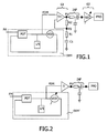
- Fig.1 presents a standard architecture of the demodulation of a modulated signal followed by an amplification of the demodulated signal obtained.
- Such a standard architecture is for example implemented and described in the data sheet of UAA3515 from Philips semiconductors.
- the demodulation is realized by a demodulator DEM using a conventional phase locked loop including a phase detector PDT, a loop filter LFI and a voltage controlled oscillator function VCO.
- the demodulated signal FDM is applied to a first amplifier stage G1 comprising a high gain amplifier G ⁇ and passive elements C1, R1 and R2.
- the use of passive elements generally implies the use of at least two connection pins P1 and P2 as shown in Fig.1 .
- the output of the amplifier stage G1 is conventionally connected using an intermediate filter INF to a second amplifier stage G2 including a complex gain control amplifier GGC.
- This second amplifier stage is then connected to a processor PRO that processes the signal so that this signal can be used.
- Such architecture presents the drawbacks that two connection pins are needed, external components are needed that are found on a PCB and moreover impose their time constant (this time constant is even greater than the R1C1 multiplication and has to be high so as not to deform the audio signal), the presence is needed of a complex gain control amplifier that often deteriorate noise floor characteristics.
- US-A-5 459 653 relates to a current controlled oscillator for use in a phase locked loop.
- Phase locked loop gain and oscillator frequency are separately digitally programmable by means of a voltage to current converter that comprises two current mirrors Each current mirror has binary weighted current mirror transistors. Respective output currents of the current mirrors are added.
- EP-A0 645 891 relates to an apparatus for frequency tuning a phase locked loop that forms part of an FM sound carrier demodulating circuit.
- the apparatus includes a signal translation circuit that provides a control voltage to a voltage controlled oscillator of the phase locked loop.
- the signal translation circuit causes the control voltage to depend on a tuning voltage, which is alterable in response to the frequency of the voltage controlled oscillator.
- the invention proposes a demodulator as claimed in claim 1, which is appended to the description.
- the demodulated frequency-modulated signals are amplified when output from the phase locked loop.
- the modifiable gain of the voltage controlled oscillator function is modifiable using a programmable transconductance.
- the voltage controlled oscillator function is controlled by the current output from the programmable transconductance.
- the programmable transconductance allows the transformation of a voltage into current, which transformation generates a current as low as amplification desires. The less important the output current of the programmable transconductance is, the most important the amplification versus the frequency variations is. This is particularly adapted to standard Intermediate Frequencies IF used in wireless communication: 450kHz, 10.7MHz.
- An advantageous implementation uses digitally programmable switches and preferentially MOS switches.
- the command of these MOS switches may then be provided by a digital command on a given number of bits for example. These bits correspond to the activation of the MOS switches.
- the invention also relates to an electronic device as claimed in claim 5 and a method of controlling a demodulator as claimed in claim 6.
- Fig.1 represents the standard architecture of a demodulator DEM followed by amplification of demodulated signals according to the state of the art in a specific second amplifier stage G2 including a complex gain control amplifier GGC. This Figure has been described above.
- FM dev is the deviation of the frequency
- f mod is the modulation frequency
- f c the central frequency of the Voltage Controlled Oscillator function VCO.
- Said central frequency f c may be the inherent oscillation frequency of an oscillator included in the function VCO or a divided-by-M own oscillation frequency of an oscillator included in the function VCO, said inherent oscillation frequency being equal to several times M of the central frequency fc, and said oscillator being followed by a divide-by-M divider.
- the function VCO is considered to include the divider. Any structure known for a voltage controlled oscillator function VCO allowing having a frequency centered on the modulation frequency of the received signals can be implemented in the state of the art and in the invention.
- the invention includes supplementary features independently of such means to center the frequency of the voltage controlled oscillator function on the modulation frequency.
- the audio processor PRO input signal is then: f dev / K VCO .
- K VCO is the gain of the VCO, this gain is fixed in the state of the art.
- G1 and G2 represent here the value gain of the two amplifier stages G1 and G2.
- the gain G2 is modifiable to adapt the amplification of the signal input in the audio processor PRO.
- the amplitude of the modification of the gain is advantageously centered on a mean value that corresponds to the most commonly required level of amplification by an exploitation system implemented at the output of the audio processor PRO.
- an exploitation system can be, for example, an earpiece with loudspeaker.
- the modification of the gain of amplifier stage G2 then enables to increase and decrease the gain around this mean value.
- This architecture presents some drawbacks.
- This architecture conventionally needs external passive elements R1, R2, C1 and two output pins in order to realize connections with those external passive elements.
- This architecture is limited in terms of settle time by the R1, C1 time constant. It has a major impact on the standby mode of a telephone for example.
- This architecture also needs a complex gain control amplifier GGC in the second amplifier stage G1.
- GGC gain control amplifier
- the DC offset of such a complex amplifier GGC limits the audio processor noise floor performances.
- the gain control is used after an output pin, the signal level on this output pin is lower than in the invention. It makes the architecture less robust to the ground audio bounce on PCB.
- the invention allows to avoid all these drawbacks by providing a high-quality demodulation and amplification of the demodulated signals with a very simple new architecture.
- the main function achieved by the invention is the demodulation of frequency-modulated signals with gain control of the output signals directly done in the phase locked loop within the voltage controlled oscillator function VCO.
- Fig.2 represents the new architecture of a demodulator DEM' with integrated gain control according to the invention.
- the phase locked loop includes a voltage controlled oscillator function VCO' with modifiable gain. This modifiable gain allows to increase or decrease the gain of the voltage controlled oscillator function VCO' to adapt the level of the input of an audio processor PRO directly in the phase locked loop.
- Such a modifiable gain voltage controlled oscillator function VCO' can be implemented in various ways.
- the voltage controlled oscillator function VCO' includes a Relaxation Oscillator RO.
- Relaxation Oscillators are known to one skilled in the art. It is constituted by a capacitor, which is charged and discharged by a current. This charge and discharge represent the period of the oscillator.
- said relaxation oscillator RO can, independently of the invention, be followed by a current divider to center the frequency of the voltage controlled oscillator function VCO' on the modulation frequency of the received signals.
- the functioning of the Relaxation Oscillator RO is controlled by the sum of two currents: I that conventionally enables the frequency of the VCO' to be centered on the modulation frequency and IGM coming from the phase locked loop and representing the frequency variations due to the frequency modulation.
- the current IGM passes through a programmable transconductance GM1.
- the transconductance GM1 has the ability to provide a dependence on the programmation data PG, more or less important current IGM for a given voltage difference between the output of said loop filter and a reference voltage VREF. Then the gain of the voltage controlled oscillator function VCO' is proportional to the value of the programmable transconductance GM1.
- Fig.4 presents a preferred use of the programmable transconductance GM1.
- Said programmable transconductance GM1 includes a fixed transconductance GM2 conventionally known in the state of the art.
- the output of this fixed transconductance is a current IGM2.
- the amplification needed is generally dedicated to adapt the level of the input signal of the audio processor in order to obtain usable signals at the output of this audio processor.
- the audio processor input signal is equal to: f dev / K VCO . G . sin 2 ⁇ ⁇ f mod ⁇ t .
- K VCO is modifiable here. Its value has to be centered on a value that enables a mean value that corresponds to the most commonly required level of amplification by an exploitation system implemented at the output of the audio processor PRO.
- the amplitude of variation of K VCO can also be determined.
- the current IGM2 is a maximum value for IGM that corresponds to a maximum of K VCO and consequently to a minimum of the audio processor input signal.
- Such a definition here means that a current equal to IGM2/ 2 n is provided on output n of the multiplier MUL, n being included in interval [1:N].
- conventional current multiplication means like current mirrors can be used in the invention.
- switches S[n] are connected to the multiplier outputs. Said switches are then linked to a summation unit SUM. The switches are controlled by programmation data PG made of n bits. It has to be noted that, in Figure 4 , a single output n and a single switch are represented for clarity. A summation unit SUM is connected to said switches.
- the summation unit SUM output current IGM is equal to IGM ⁇ 2 ⁇ ⁇ n / PG 1 / 2 n .
- Said outputs can also be permanently connected to the summation unit SUM.
- the summation unit SUM can sum as many currents as there are permanently connected outputs, or outputs connected via a switch. Any combination of the outputs of the multiplier MUL is possible according to the invention. Any kind of output of a multiplier may also be used according to the invention. Multiplier MUL outputs may be any kind of multiple of the multiplier input current IGM2. Amplitude of modification of IGM is then defined by an interval of current, defined by limits that can be taken by the sum. Said interval is advantageously centered on the above-invoked mean value.
- IGM2 is a minimum value that corresponds to the higher possible required gain.
- the multiplier for example, provides IGM2 and the summation is an integer multiple of IGM2.
- a multiplier according to the invention can also provide any multiple of IGM2 at its outputs, said multiples being then summed according to the invention.
- IGM IGM ⁇ 2 ⁇ ⁇ n / PG 2 n - 1 .
- the voltage controlled oscillator function VCO' includes a multiplier.
- the modification of the gain of the voltage controlled oscillator function VCO' is then realized using commutation of currents.
- the decreasing of the gain results in an amplification of the frequency variations in the Relaxation Oscillator VCO for a given signal. Consequently, the formed demodulated signal FDM is amplified in a customizable way regarding what would have been obtained with a fixed transconductance GM2.
- the change of the gain of the voltage controlled oscillator function VCO' generates a change in the output gain. It has to be noted that the gain of the amplifier of the first amplifier stage in the architecture of the state of the art has to be high (conventionally around 20) while the gain of G needs generally to be around 1 or 2.
- the invention enables to reduce the time necessary to establish a balance in the receiving chain of a reception device compared to the state of the art. Effectively, the invention allows not to be limited by the time constant of external elements. The invention allows not to have external elements. The invention allows to reduce the silicon size required to realize functions of gain control amplification more than 100 times (no complex gain control amplifier). The invention allows not to need a complex gain control amplifier.
- the DC offset of the latter amplifier induces limitations in the noise floor performance of the audio processor. According to the invention, the DC offset of the amplification is removed before the audio processor by the AC coupling realized by the filter INF in Figure 2 . As the gain control is implemented before the output pin, the signal level on this pin is higher than in the state-of-the-art architecture. It makes the architecture more robust relative to the ground audio bounce on PCB.
- the new architecture according to the invention provides an amplification equivalent to the one realized in the state of the art without having the drawbacks of the latter.
- the invention allows improvements concerning silicon occupation, audio quality, pinning count, external components and PCB area.
- System consumption is also reduced as the settling time of the receiver is reduced (no more time constant). Effectively, the standby time being reduced, the consumption is reduced.
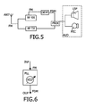
- Fig.5 illustrates a receiving device according to the invention.
- This Figure is a highly schematic representation of such a receiving device. It includes at least an antenna ANT at least able to receive frequency-modulated signals FM (Radio-Frequency RF or other), a demodulator DEM' according to the invention, a receiving chain RX with a processing unit PROC. Said receiving chain RX and demodulator DEM' are advantageously connected to an audio system AUD and allow the use of demodulated signals FDM. This can be an earpiece with a loudspeaker LSP.
- the receiving device also includes a transmission chain TX advantageously linked to the processing unit PROC and to the audio system AUD. This is the case with telephone for example. Then the audio system also includes a microphone MIC for example.
- Fig.6 is a block diagram of a method to demodulate a signal according to the invention, said block diagram also describing schematically the invention according to the abstract.
- a method for demodulating frequency-modulated signals according to the invention includes the step INP of applying frequency-modulated signals FM to an input of a phase locked loop PLL which includes at least a phase detector, a loop filter and a Voltage controlled oscillator function VCO', the step of amplifying frequency variations by modifying/decreasing gain of the voltage controlled oscillator function VCO', said voltage controlled oscillator function VCO' having a modifiable gain, the step OUP of producing demodulated signals FDM at an output of the phase locked loop PLL.
Landscapes
- Engineering & Computer Science (AREA)
- Power Engineering (AREA)
- Stabilization Of Oscillater, Synchronisation, Frequency Synthesizers (AREA)
- Circuits Of Receivers In General (AREA)
- Superheterodyne Receivers (AREA)
Claims (6)
- Demodulator (DEM') zum Demodulieren frequenzmodulierter Signale, wobei der Demodulator einen Phasenregelkreis bzw. -schleife mit zumindest einem Phasendetektor (PDT), einem Schleifenfilter (LFI) und einer spannungsgesteuerten bzw. -geregelten Oszillatorfunktion (VCO') umfasst, dadurch gekennzeichnet, dass die spannungsgesteuerte bzw. -geregelte Oszillatorfunktion (VCO') einen Relaxationsoszillator (RO) enthält und eine modifizierbare Verstärkung bzw. Verstärkungsfaktor mittels bzw. durch eine programmierbare Transkonduktanz bzw. Steilheit (GM1) aufweist, wobei der Demodulator eine Verstärkungssteuerung bzw. -regelung umfasst, um den Pegel bzw. die Stärke eines Ausgangssignals des Demodulators anzupassen, indem sie die Verstärkung der spannungsgesteuerten bzw. -geregelten Oszillatorfunktion modifiziert.
- Demodulator nach Anspruch 1, wobei die programmierbare Transkonduktanz (GM1) eine feste Transkonduktanz bzw. Steilheit (GM2), einen Stromvervielfacher bzw. -multiplikator (MUL) enthält, wobei der Ausgang bzw. die Ausgabe der programmierbaren Transkonduktanz der Ausgang bzw. die Ausgabe einer Summierungseinheit (SUM) ist, die eine Kombination zumindest eines Ausgangs bzw. einer Ausgabe des Vervielfachers summiert.
- Demodulator nach Anspruch 2, wobei digital programmierbare Schalter zwischen den Stromvervielfacher (MUL) und die Summierungseinheit (SUM) gekoppelt sind.
- Demodulator nach Anspruch 3, wobei die Schalter MOS-Schalter sind.
- Elektronische Vorrichtung, die in der Lage ist, frequenzmodulierte Signale zu empfangen, dadurch gekennzeichnet, dass die Demodulation der Signale durch einen Demodulator nach einem der Ansprüche 1 bis 4 realisiert wird.
- Verfahren zum Steuern bzw. Regeln eines Demodulators (DEM') zum Demodulieren frequenzmodulierter Signale, wobei der Demodulator einen Phasenregelkreis bzw. -schleife mit zumindest einem Phasendetektor (PDT), einem Schleifenfilter (LFI) und einer spannungsgesteuerten bzw. -geregelten Oszillatorfunktion (VCO') umfasst, dadurch gekennzeichnet, dass die spannungsgesteuerte bzw. -geregelte Oszillatorfunktion (VCO') einen Relaxationsoszillator (RO) enthält und eine modifizierbare Verstärkung bzw. Verstärkungsfaktor mittels bzw. durch eine programmierbare Transkonduktanz bzw. Steilheit (GM1) aufweist, wobei das Verfahren den Schritt des Anpassens des Pegels bzw. der Stärke eines Ausgangssignals des Demodulators umfasst, dadurch dass die Verstärkung der spannungsgesteuerten bzw. -geregelten Oszillatorfunktion modifiziert wird.
Priority Applications (1)
| Application Number | Priority Date | Filing Date | Title |
|---|---|---|---|
| EP03748441A EP1568124B1 (de) | 2002-10-30 | 2003-10-09 | Phasenregelkreisdemodulator mit automatischer verstärkungsregelung |
Applications Claiming Priority (4)
| Application Number | Priority Date | Filing Date | Title |
|---|---|---|---|
| EP02292708 | 2002-10-30 | ||
| EP02292708 | 2002-10-30 | ||
| PCT/IB2003/004508 WO2004040749A1 (en) | 2002-10-30 | 2003-10-09 | Phase locked loop demodulator with gain control |
| EP03748441A EP1568124B1 (de) | 2002-10-30 | 2003-10-09 | Phasenregelkreisdemodulator mit automatischer verstärkungsregelung |
Publications (2)
| Publication Number | Publication Date |
|---|---|
| EP1568124A1 EP1568124A1 (de) | 2005-08-31 |
| EP1568124B1 true EP1568124B1 (de) | 2009-04-22 |
Family
ID=32187268
Family Applications (1)
| Application Number | Title | Priority Date | Filing Date |
|---|---|---|---|
| EP03748441A Expired - Lifetime EP1568124B1 (de) | 2002-10-30 | 2003-10-09 | Phasenregelkreisdemodulator mit automatischer verstärkungsregelung |
Country Status (8)
| Country | Link |
|---|---|
| US (1) | US7420409B2 (de) |
| EP (1) | EP1568124B1 (de) |
| JP (1) | JP2006505176A (de) |
| CN (1) | CN100459415C (de) |
| AT (1) | ATE429730T1 (de) |
| AU (1) | AU2003267746A1 (de) |
| DE (1) | DE60327360D1 (de) |
| WO (1) | WO2004040749A1 (de) |
Families Citing this family (2)
| Publication number | Priority date | Publication date | Assignee | Title |
|---|---|---|---|---|
| TW201709155A (zh) * | 2015-07-09 | 2017-03-01 | 美高森美半導體美國公司 | 音響警報偵測器 |
| TWI617141B (zh) * | 2016-07-01 | 2018-03-01 | 晨星半導體股份有限公司 | 調頻接收器以及調頻接收方法 |
Family Cites Families (12)
| Publication number | Priority date | Publication date | Assignee | Title |
|---|---|---|---|---|
| CA1325251C (en) * | 1988-09-02 | 1993-12-14 | Shigeki Saito | Frequency synthesizer |
| US5369376A (en) * | 1991-11-29 | 1994-11-29 | Standard Microsystems, Inc. | Programmable phase locked loop circuit and method of programming same |
| FR2684772B1 (fr) * | 1991-12-10 | 1994-08-26 | Thomson Csf | Reseau d'indice optique commandable electriquement. |
| US5459653A (en) * | 1993-06-23 | 1995-10-17 | Ati Technologies Inc. | Voltage to current converter with independent loop gain and frequency control |
| GB9320069D0 (en) * | 1993-09-29 | 1993-11-17 | Sgs Thomson Microelectronics | Frequency tuning for a phase locked loop |
| US5604926A (en) * | 1995-03-07 | 1997-02-18 | Motorola, Inc. | Phase locked loop circuit current mode feedback |
| FR2737626B1 (fr) * | 1995-07-31 | 1997-09-05 | Sgs Thomson Microelectronics | Dispositif et procede pour regler la frequence d'accord d'un demodulateur pll |
| JPH1188051A (ja) * | 1997-09-12 | 1999-03-30 | Hitachi Ltd | 発振器 |
| JPH11195982A (ja) * | 1998-01-06 | 1999-07-21 | Nec Corp | Pll回路 |
| JP3212942B2 (ja) * | 1998-04-24 | 2001-09-25 | 日本電気株式会社 | Pll(位相ロックループ)回路 |
| US6404294B1 (en) * | 2000-07-18 | 2002-06-11 | Cypress Semiconductor Corp. | Voltage control oscillator (VCO) with automatic gain control |
| US6583675B2 (en) * | 2001-03-20 | 2003-06-24 | Broadcom Corporation | Apparatus and method for phase lock loop gain control using unit current sources |
-
2003
- 2003-10-09 EP EP03748441A patent/EP1568124B1/de not_active Expired - Lifetime
- 2003-10-09 CN CNB2003801026846A patent/CN100459415C/zh not_active Expired - Lifetime
- 2003-10-09 AT AT03748441T patent/ATE429730T1/de not_active IP Right Cessation
- 2003-10-09 US US10/532,902 patent/US7420409B2/en not_active Expired - Lifetime
- 2003-10-09 AU AU2003267746A patent/AU2003267746A1/en not_active Abandoned
- 2003-10-09 JP JP2004547863A patent/JP2006505176A/ja not_active Withdrawn
- 2003-10-09 WO PCT/IB2003/004508 patent/WO2004040749A1/en not_active Ceased
- 2003-10-09 DE DE60327360T patent/DE60327360D1/de not_active Expired - Lifetime
Also Published As
| Publication number | Publication date |
|---|---|
| DE60327360D1 (de) | 2009-06-04 |
| JP2006505176A (ja) | 2006-02-09 |
| CN1711676A (zh) | 2005-12-21 |
| US7420409B2 (en) | 2008-09-02 |
| EP1568124A1 (de) | 2005-08-31 |
| US20060071708A1 (en) | 2006-04-06 |
| AU2003267746A1 (en) | 2004-05-25 |
| CN100459415C (zh) | 2009-02-04 |
| ATE429730T1 (de) | 2009-05-15 |
| WO2004040749A1 (en) | 2004-05-13 |
Similar Documents
| Publication | Publication Date | Title |
|---|---|---|
| KR100314798B1 (ko) | 집적화된이미지제거믹서 | |
| US7002403B2 (en) | Transconductance/C complex band-pass filter | |
| US20020044621A1 (en) | Phase-locked loop circuit and radio communication apparatus using the same | |
| EP0196697B1 (de) | AM-Empfänger | |
| JPH0691477B2 (ja) | Rf同調回路 | |
| JP3164008B2 (ja) | 無線受信機 | |
| JP3866290B2 (ja) | 信号のオフセット電圧を低減させる方法および回路装置 | |
| JPH11284489A (ja) | 積分フィルタ回路 | |
| US6184747B1 (en) | Differential filter with gyrator | |
| US7266351B2 (en) | Transconductance / C complex band-pass filter | |
| US20030202616A1 (en) | Radio receiver utilizing a single analog to digital converter | |
| EP1568124B1 (de) | Phasenregelkreisdemodulator mit automatischer verstärkungsregelung | |
| JP3108744B2 (ja) | ノイズ防止回路 | |
| US7027505B2 (en) | System and method for bandwidth compression of frequency and phase modulated signals and suppression of the upper and lower sidebands from the transmission medium | |
| US6943618B1 (en) | Compensation mechanism for compensating bias levels of an operation circuit in response to supply voltage changes | |
| JPH104372A (ja) | 多モード無線電話 | |
| EP1489752A1 (de) | Empfängervorrichtung | |
| US7493097B2 (en) | High dynamic range compact mixer output stage for a wireless receiver | |
| EP1557941A1 (de) | Filterschaltung und funkgerät | |
| EP0519562B1 (de) | Empfänger mit einer Phasenregelschleife | |
| KR20010093263A (ko) | 개량된 다위상 수신기 | |
| US20040198278A1 (en) | On-chip loop filter for use in a phase locked loop and other applications | |
| US5650714A (en) | Orthogonal signal generation system | |
| US7403962B2 (en) | Interpolation filter design and application | |
| US20070035354A1 (en) | Dual port modulator |
Legal Events
| Date | Code | Title | Description |
|---|---|---|---|
| PUAI | Public reference made under article 153(3) epc to a published international application that has entered the european phase |
Free format text: ORIGINAL CODE: 0009012 |
|
| 17P | Request for examination filed |
Effective date: 20050530 |
|
| AK | Designated contracting states |
Kind code of ref document: A1 Designated state(s): AT BE BG CH CY CZ DE DK EE ES FI FR GB GR HU IE IT LI LU MC NL PT RO SE SI SK TR |
|
| AX | Request for extension of the european patent |
Extension state: AL LT LV MK |
|
| DAX | Request for extension of the european patent (deleted) | ||
| RAP1 | Party data changed (applicant data changed or rights of an application transferred) |
Owner name: NXP B.V. |
|
| RAP1 | Party data changed (applicant data changed or rights of an application transferred) |
Owner name: DSP GROUP SWITZERLAND AG |
|
| GRAJ | Information related to disapproval of communication of intention to grant by the applicant or resumption of examination proceedings by the epo deleted |
Free format text: ORIGINAL CODE: EPIDOSDIGR1 |
|
| GRAP | Despatch of communication of intention to grant a patent |
Free format text: ORIGINAL CODE: EPIDOSNIGR1 |
|
| GRAP | Despatch of communication of intention to grant a patent |
Free format text: ORIGINAL CODE: EPIDOSNIGR1 |
|
| GRAS | Grant fee paid |
Free format text: ORIGINAL CODE: EPIDOSNIGR3 |
|
| GRAA | (expected) grant |
Free format text: ORIGINAL CODE: 0009210 |
|
| AK | Designated contracting states |
Kind code of ref document: B1 Designated state(s): AT BE BG CH CY CZ DE DK EE ES FI FR GB GR HU IE IT LI LU MC NL PT RO SE SI SK TR |
|
| REG | Reference to a national code |
Ref country code: GB Ref legal event code: FG4D |
|
| REG | Reference to a national code |
Ref country code: CH Ref legal event code: EP |
|
| REG | Reference to a national code |
Ref country code: IE Ref legal event code: FG4D |
|
| REF | Corresponds to: |
Ref document number: 60327360 Country of ref document: DE Date of ref document: 20090604 Kind code of ref document: P |
|
| NLV1 | Nl: lapsed or annulled due to failure to fulfill the requirements of art. 29p and 29m of the patents act | ||
| PG25 | Lapsed in a contracting state [announced via postgrant information from national office to epo] |
Ref country code: PT Free format text: LAPSE BECAUSE OF FAILURE TO SUBMIT A TRANSLATION OF THE DESCRIPTION OR TO PAY THE FEE WITHIN THE PRESCRIBED TIME-LIMIT Effective date: 20090822 Ref country code: ES Free format text: LAPSE BECAUSE OF FAILURE TO SUBMIT A TRANSLATION OF THE DESCRIPTION OR TO PAY THE FEE WITHIN THE PRESCRIBED TIME-LIMIT Effective date: 20090802 Ref country code: AT Free format text: LAPSE BECAUSE OF FAILURE TO SUBMIT A TRANSLATION OF THE DESCRIPTION OR TO PAY THE FEE WITHIN THE PRESCRIBED TIME-LIMIT Effective date: 20090422 Ref country code: FI Free format text: LAPSE BECAUSE OF FAILURE TO SUBMIT A TRANSLATION OF THE DESCRIPTION OR TO PAY THE FEE WITHIN THE PRESCRIBED TIME-LIMIT Effective date: 20090422 |
|
| PG25 | Lapsed in a contracting state [announced via postgrant information from national office to epo] |
Ref country code: SI Free format text: LAPSE BECAUSE OF FAILURE TO SUBMIT A TRANSLATION OF THE DESCRIPTION OR TO PAY THE FEE WITHIN THE PRESCRIBED TIME-LIMIT Effective date: 20090422 Ref country code: NL Free format text: LAPSE BECAUSE OF FAILURE TO SUBMIT A TRANSLATION OF THE DESCRIPTION OR TO PAY THE FEE WITHIN THE PRESCRIBED TIME-LIMIT Effective date: 20090422 Ref country code: SE Free format text: LAPSE BECAUSE OF FAILURE TO SUBMIT A TRANSLATION OF THE DESCRIPTION OR TO PAY THE FEE WITHIN THE PRESCRIBED TIME-LIMIT Effective date: 20090722 |
|
| PG25 | Lapsed in a contracting state [announced via postgrant information from national office to epo] |
Ref country code: RO Free format text: LAPSE BECAUSE OF FAILURE TO SUBMIT A TRANSLATION OF THE DESCRIPTION OR TO PAY THE FEE WITHIN THE PRESCRIBED TIME-LIMIT Effective date: 20090422 Ref country code: EE Free format text: LAPSE BECAUSE OF FAILURE TO SUBMIT A TRANSLATION OF THE DESCRIPTION OR TO PAY THE FEE WITHIN THE PRESCRIBED TIME-LIMIT Effective date: 20090422 Ref country code: DK Free format text: LAPSE BECAUSE OF FAILURE TO SUBMIT A TRANSLATION OF THE DESCRIPTION OR TO PAY THE FEE WITHIN THE PRESCRIBED TIME-LIMIT Effective date: 20090422 Ref country code: CZ Free format text: LAPSE BECAUSE OF FAILURE TO SUBMIT A TRANSLATION OF THE DESCRIPTION OR TO PAY THE FEE WITHIN THE PRESCRIBED TIME-LIMIT Effective date: 20090422 |
|
| PG25 | Lapsed in a contracting state [announced via postgrant information from national office to epo] |
Ref country code: BE Free format text: LAPSE BECAUSE OF FAILURE TO SUBMIT A TRANSLATION OF THE DESCRIPTION OR TO PAY THE FEE WITHIN THE PRESCRIBED TIME-LIMIT Effective date: 20090422 Ref country code: SK Free format text: LAPSE BECAUSE OF FAILURE TO SUBMIT A TRANSLATION OF THE DESCRIPTION OR TO PAY THE FEE WITHIN THE PRESCRIBED TIME-LIMIT Effective date: 20090422 |
|
| PLBE | No opposition filed within time limit |
Free format text: ORIGINAL CODE: 0009261 |
|
| STAA | Information on the status of an ep patent application or granted ep patent |
Free format text: STATUS: NO OPPOSITION FILED WITHIN TIME LIMIT |
|
| 26N | No opposition filed |
Effective date: 20100125 |
|
| PG25 | Lapsed in a contracting state [announced via postgrant information from national office to epo] |
Ref country code: BG Free format text: LAPSE BECAUSE OF FAILURE TO SUBMIT A TRANSLATION OF THE DESCRIPTION OR TO PAY THE FEE WITHIN THE PRESCRIBED TIME-LIMIT Effective date: 20090722 |
|
| PG25 | Lapsed in a contracting state [announced via postgrant information from national office to epo] |
Ref country code: MC Free format text: LAPSE BECAUSE OF NON-PAYMENT OF DUE FEES Effective date: 20091031 |
|
| REG | Reference to a national code |
Ref country code: CH Ref legal event code: PL |
|
| REG | Reference to a national code |
Ref country code: IE Ref legal event code: MM4A |
|
| PG25 | Lapsed in a contracting state [announced via postgrant information from national office to epo] |
Ref country code: LI Free format text: LAPSE BECAUSE OF NON-PAYMENT OF DUE FEES Effective date: 20091031 Ref country code: CH Free format text: LAPSE BECAUSE OF NON-PAYMENT OF DUE FEES Effective date: 20091031 Ref country code: GR Free format text: LAPSE BECAUSE OF FAILURE TO SUBMIT A TRANSLATION OF THE DESCRIPTION OR TO PAY THE FEE WITHIN THE PRESCRIBED TIME-LIMIT Effective date: 20090723 Ref country code: IE Free format text: LAPSE BECAUSE OF NON-PAYMENT OF DUE FEES Effective date: 20091009 |
|
| PG25 | Lapsed in a contracting state [announced via postgrant information from national office to epo] |
Ref country code: IT Free format text: LAPSE BECAUSE OF FAILURE TO SUBMIT A TRANSLATION OF THE DESCRIPTION OR TO PAY THE FEE WITHIN THE PRESCRIBED TIME-LIMIT Effective date: 20090422 |
|
| PG25 | Lapsed in a contracting state [announced via postgrant information from national office to epo] |
Ref country code: LU Free format text: LAPSE BECAUSE OF NON-PAYMENT OF DUE FEES Effective date: 20091009 |
|
| PG25 | Lapsed in a contracting state [announced via postgrant information from national office to epo] |
Ref country code: HU Free format text: LAPSE BECAUSE OF FAILURE TO SUBMIT A TRANSLATION OF THE DESCRIPTION OR TO PAY THE FEE WITHIN THE PRESCRIBED TIME-LIMIT Effective date: 20091023 |
|
| PG25 | Lapsed in a contracting state [announced via postgrant information from national office to epo] |
Ref country code: TR Free format text: LAPSE BECAUSE OF FAILURE TO SUBMIT A TRANSLATION OF THE DESCRIPTION OR TO PAY THE FEE WITHIN THE PRESCRIBED TIME-LIMIT Effective date: 20090422 |
|
| PG25 | Lapsed in a contracting state [announced via postgrant information from national office to epo] |
Ref country code: CY Free format text: LAPSE BECAUSE OF FAILURE TO SUBMIT A TRANSLATION OF THE DESCRIPTION OR TO PAY THE FEE WITHIN THE PRESCRIBED TIME-LIMIT Effective date: 20090422 |
|
| REG | Reference to a national code |
Ref country code: FR Ref legal event code: PLFP Year of fee payment: 13 |
|
| REG | Reference to a national code |
Ref country code: FR Ref legal event code: PLFP Year of fee payment: 14 |
|
| REG | Reference to a national code |
Ref country code: FR Ref legal event code: PLFP Year of fee payment: 15 |
|
| REG | Reference to a national code |
Ref country code: FR Ref legal event code: PLFP Year of fee payment: 16 |
|
| PGFP | Annual fee paid to national office [announced via postgrant information from national office to epo] |
Ref country code: GB Payment date: 20220922 Year of fee payment: 20 |
|
| REG | Reference to a national code |
Ref country code: DE Ref legal event code: R082 Ref document number: 60327360 Country of ref document: DE |
|
| PGFP | Annual fee paid to national office [announced via postgrant information from national office to epo] |
Ref country code: FR Payment date: 20220920 Year of fee payment: 20 |
|
| PGFP | Annual fee paid to national office [announced via postgrant information from national office to epo] |
Ref country code: DE Payment date: 20220920 Year of fee payment: 20 |
|
| REG | Reference to a national code |
Ref country code: DE Ref legal event code: R071 Ref document number: 60327360 Country of ref document: DE |
|
| REG | Reference to a national code |
Ref country code: GB Ref legal event code: PE20 Expiry date: 20231008 |
|
| PG25 | Lapsed in a contracting state [announced via postgrant information from national office to epo] |
Ref country code: GB Free format text: LAPSE BECAUSE OF EXPIRATION OF PROTECTION Effective date: 20231008 |
|
| PG25 | Lapsed in a contracting state [announced via postgrant information from national office to epo] |
Ref country code: GB Free format text: LAPSE BECAUSE OF EXPIRATION OF PROTECTION Effective date: 20231008 |