EP1566886A2 - Leistungsverstärker und Mobilkommunikationsendgerät - Google Patents
Leistungsverstärker und Mobilkommunikationsendgerät Download PDFInfo
- Publication number
- EP1566886A2 EP1566886A2 EP05250943A EP05250943A EP1566886A2 EP 1566886 A2 EP1566886 A2 EP 1566886A2 EP 05250943 A EP05250943 A EP 05250943A EP 05250943 A EP05250943 A EP 05250943A EP 1566886 A2 EP1566886 A2 EP 1566886A2
- Authority
- EP
- European Patent Office
- Prior art keywords
- amplification
- fet
- terminal
- power
- amplification element
- Prior art date
- Legal status (The legal status is an assumption and is not a legal conclusion. Google has not performed a legal analysis and makes no representation as to the accuracy of the status listed.)
- Withdrawn
Links
Images


Classifications
-
- H—ELECTRICITY
- H03—ELECTRONIC CIRCUITRY
- H03F—AMPLIFIERS
- H03F1/00—Details of amplifiers with only discharge tubes, only semiconductor devices or only unspecified devices as amplifying elements
- H03F1/02—Modifications of amplifiers to raise the efficiency, e.g. gliding Class A stages, use of an auxiliary oscillation
-
- E—FIXED CONSTRUCTIONS
- E04—BUILDING
- E04G—SCAFFOLDING; FORMS; SHUTTERING; BUILDING IMPLEMENTS OR AIDS, OR THEIR USE; HANDLING BUILDING MATERIALS ON THE SITE; REPAIRING, BREAKING-UP OR OTHER WORK ON EXISTING BUILDINGS
- E04G7/00—Connections between parts of the scaffold
- E04G7/02—Connections between parts of the scaffold with separate coupling elements
- E04G7/28—Clips or connections for securing boards
-
- E—FIXED CONSTRUCTIONS
- E04—BUILDING
- E04G—SCAFFOLDING; FORMS; SHUTTERING; BUILDING IMPLEMENTS OR AIDS, OR THEIR USE; HANDLING BUILDING MATERIALS ON THE SITE; REPAIRING, BREAKING-UP OR OTHER WORK ON EXISTING BUILDINGS
- E04G21/00—Preparing, conveying, or working-up building materials or building elements in situ; Other devices or measures for constructional work
- E04G21/32—Safety or protective measures for persons during the construction of buildings
-
- E—FIXED CONSTRUCTIONS
- E04—BUILDING
- E04G—SCAFFOLDING; FORMS; SHUTTERING; BUILDING IMPLEMENTS OR AIDS, OR THEIR USE; HANDLING BUILDING MATERIALS ON THE SITE; REPAIRING, BREAKING-UP OR OTHER WORK ON EXISTING BUILDINGS
- E04G7/00—Connections between parts of the scaffold
- E04G7/30—Scaffolding bars or members with non-detachably fixed coupling elements
- E04G7/34—Scaffolding bars or members with non-detachably fixed coupling elements with coupling elements using positive engagement, e.g. hooks or pins
-
- H—ELECTRICITY
- H03—ELECTRONIC CIRCUITRY
- H03F—AMPLIFIERS
- H03F1/00—Details of amplifiers with only discharge tubes, only semiconductor devices or only unspecified devices as amplifying elements
- H03F1/02—Modifications of amplifiers to raise the efficiency, e.g. gliding Class A stages, use of an auxiliary oscillation
- H03F1/0205—Modifications of amplifiers to raise the efficiency, e.g. gliding Class A stages, use of an auxiliary oscillation in transistor amplifiers
- H03F1/0277—Selecting one or more amplifiers from a plurality of amplifiers
-
- H—ELECTRICITY
- H03—ELECTRONIC CIRCUITRY
- H03F—AMPLIFIERS
- H03F1/00—Details of amplifiers with only discharge tubes, only semiconductor devices or only unspecified devices as amplifying elements
- H03F1/08—Modifications of amplifiers to reduce detrimental influences of internal impedances of amplifying elements
- H03F1/22—Modifications of amplifiers to reduce detrimental influences of internal impedances of amplifying elements by use of cascode coupling, i.e. earthed cathode or emitter stage followed by earthed grid or base stage respectively
- H03F1/223—Modifications of amplifiers to reduce detrimental influences of internal impedances of amplifying elements by use of cascode coupling, i.e. earthed cathode or emitter stage followed by earthed grid or base stage respectively with MOSFET's
-
- H—ELECTRICITY
- H03—ELECTRONIC CIRCUITRY
- H03F—AMPLIFIERS
- H03F3/00—Amplifiers with only discharge tubes or only semiconductor devices as amplifying elements
- H03F3/20—Power amplifiers, e.g. Class B amplifiers, Class C amplifiers
- H03F3/24—Power amplifiers, e.g. Class B amplifiers, Class C amplifiers of transmitter output stages
-
- H—ELECTRICITY
- H03—ELECTRONIC CIRCUITRY
- H03F—AMPLIFIERS
- H03F3/00—Amplifiers with only discharge tubes or only semiconductor devices as amplifying elements
- H03F3/72—Gated amplifiers, i.e. amplifiers which are rendered operative or inoperative by means of a control signal
-
- H—ELECTRICITY
- H03—ELECTRONIC CIRCUITRY
- H03G—CONTROL OF AMPLIFICATION
- H03G1/00—Details of arrangements for controlling amplification
- H03G1/0005—Circuits characterised by the type of controlling devices operated by a controlling current or voltage signal
- H03G1/0088—Circuits characterised by the type of controlling devices operated by a controlling current or voltage signal using discontinuously variable devices, e.g. switch-operated
-
- H—ELECTRICITY
- H04—ELECTRIC COMMUNICATION TECHNIQUE
- H04B—TRANSMISSION
- H04B1/00—Details of transmission systems, not covered by a single one of groups H04B3/00 - H04B13/00; Details of transmission systems not characterised by the medium used for transmission
- H04B1/02—Transmitters
- H04B1/04—Circuits
- H04B2001/0408—Circuits with power amplifiers
- H04B2001/045—Circuits with power amplifiers with means for improving efficiency
Definitions
- the present invention relates to a power amplification apparatus which are suitable for application (by way of non-limiting example) to a mobile telephone, a PHS phone (Personal Handy-phone System), a PDA apparatus (Personal Digital Assistant) provided with a communication function, and a terminal apparatus such as a note-type personal computer using a communication function, and a mobile communication terminal apparatus.
- a power amplification apparatus which are suitable for application (by way of non-limiting example) to a mobile telephone, a PHS phone (Personal Handy-phone System), a PDA apparatus (Personal Digital Assistant) provided with a communication function, and a terminal apparatus such as a note-type personal computer using a communication function, and a mobile communication terminal apparatus.
- a mobile radio communication system using the PDC, CDMA methods or the like such communication is secured between a mobile terminal and a base station by establishing a radio channel there-between.
- a signal level will change from time to time. Therefore, in a transmission system of the mobile terminal, it is arranged such that after adjusting a transmission signal to a desired signal level in a power amplifier, the signal is transmitted to the base station.
- a patent document 1 Japanese Laid-Open Patent H9-130275 discloses a gain adjusting method for a transmission signal to achieve an improvement of an operation efficiency in a power amplification apparatus while suppressing unnecessary power consumption by selecting a signal path including signal amplification means having a gain corresponding to a desired signal level among a plurality of signal paths each including signal amplification means having a different gain, by amplifying and outputting the transmission signal with the gain of the signal amplification means of selected signal path, and by stop-controlling the operation of the signal amplification means of non-selected signal paths.
- Patent Document 1 Japanese Laid-Open Patent H9-130275
- a recent mobile phone is added with many functions of a so-called application such as a present location detection function with a GPS (Global Positioning System) sensor, a TV signal receiving function, an infrared communication function, a TV telephone function with a camera and the like. Therefore, an occasion of performing a high speed communication with the base station is increasing, and also a period of time for performing this high speed communication is prolonging. Thereby, an average transmission power is increasing to more than 10 mW, and thus it is required more and more to enable to deliver a transmission power which is amplified to a large power without causing any loss.
- GPS Global Positioning System
- the present invention has been contemplated in consideration of the above-mentioned problems, and at least preferred embodiments thereof are configured to provide a power amplification apparatus and a mobile communication terminal apparatus which are capable of remarkably improving the operation efficiency, and further capable of integrating to be one-chip form.
- One embodiment of a power amplification apparatus includes a first amplification element for amplifying an input signal, and a second amplification element for further amplifying the input signal amplified in the first amplification element and supplying to a first output terminal.
- this embodiment further includes a first switch element performing on/off operation based on a control signal for-setting the second amplification element in an operating condition by supplying the input signal from the first amplification element when on operation, and setting the second amplification element in an non-operating condition by not supplying the input signal from the first amplification element when off operation, and second switch element performing on/off operation based on a control signal but opposite to the operation of the first switch element for supplying the input signal from the first amplification element to a second output terminal when on operation, and for stopping the supply of the input signal to the second output terminal when off operation.
- the first switch element and the second switch element are operated in opposite relation to each other by a control signal. Specifically, when outputting a large power, the first switch element is controlled to be ON, and the second switch element is controlled to be OFF by the control signal.
- the input signal from the first amplification element is supplied to the second amplification element, the second amplification element is controlled to be ON-state, and the input signal amplified in multi-stage in the first amplification element and the second amplification element to be a large power is outputted.
- the first switch element is controlled to be OFF, and the second switch element is controlled to be ON by the control signal.
- the supply of the input signal from the first amplification element to the second amplification element is stopped, the second amplification element is controlled to be stopped condition, and the input signal amplified only by the first amplification element to be a medium power is outputted.
- the amplification element (the second amplification element) in a later stage is made in operating condition when outputting a large power, and the amplification element in the later stage is stopped its operation when outputting a medium power, so that it is possible to improve a total operation efficiency of this power amplification apparatus.
- the first amplification element, the second amplification element, the first switch element, and the second switch element are formed by forming a high mobility electron channel near a hetero-junction between two semiconductor layers of a plurality of semiconductor layers stacked on a semiconductor substrate for forming a channel of a transistor, forming a contact semiconductor layer, which is a high mobility electron transistor having a gate electrode and is made of impurity doped semiconductor material, on at least one side surface of the plurality of the semiconductor layers, and forming a high mobility electron transistor a source electrode or a drain electrode of which is formed through an ohmic contact layer on the contact semiconductor layer.
- the contact semiconductor layer is formed on a side surface of the plurality of semiconductor layers (a hetero-structure), and the ohmic contact layer is formed on the contact semiconductor layer. Accordingly, it is possible to reduce ON-resistance because there is no barrier layer having a high resistance within an operation current path.
- the contact semiconductor layer is made of conductive semiconductor material and is extended up to an upper surface of the hetero-structure, an ohmic contact is possible at this portion, and it is not necessary to dig the semiconductor material deeply by etching. Therefore, even the operation current is bypassed out of the barrier layer by providing the contact semiconductor layer, the increase of the occupied area is very few.
- the power amplification apparatus is able to be configured to be one-chip form by applying the high mobility electron transistor as the first amplification element, the second amplification element, the first switch element, and the second switch element.
- the present invention it is possible to remarkably improve the operation efficiency of the power amplification apparatus. Further, it is able to integrate the power amplification apparatus into one-chip form.
- the present invention is applicable to a mobile phone based on a W-CDMA (Wideband-Code Division Multiple Access) format as shown in FIG. 1.
- W-CDMA Wideband-Code Division Multiple Access
- a mobile phone receives a radio frequency signal transmitted from a base station through an antenna 1 at the time of its receiving.
- the radio frequency signal received through this antenna 1 is supplied to a receiver circuit 3 (RX) through an antenna duplexer (DUP) 2.
- RX receiver circuit 3
- DUP antenna duplexer
- the receiver circuit 3 converts a radio frequency signal to an intermediate frequency signal by mixing a receiver local oscillation signal supplied from a frequency synthesizer (SYN) 4 with the radio frequency signal received through the antenna 1, and supplies it to a CDMA signal processing unit 6.
- a frequency of the receiver local oscillation signal outputted from the frequency synthesizer 4 is controlled in response to a control signal from the control unit 5.
- the CDMA signal processing unit 6 applies an orthogonal demodulation processing to the received intermediate frequency signal as well as a de-spreading processing thereto using a spread code (PN code) assigned to a reception channel so as to convert the received intermediate frequency signal to a received data in a predetermined format corresponding to its data rate then to be supplied to a code processing unit 7.
- PN code spread code
- the CDMA signal processing unit 6 supplies information indicating a data rate of the received data to the control unit 5 as a received data rate.
- the code processing unit 7 after applying a compression/decompression processing to the received data supplied from the CDMA signal processing unit 6 on the basis of a received data rate notified from the control unit 5, carries out a demodulation processing and an error correction demodulation processing using a Viterbi decoder or the like to reproduce the received data in a base band.
- a PCM code processing unit 8 carries out a different signal processing depending on a type of communication (a voice communication or data communication) discriminated in the control unit 5.
- the PCM code processing unit 8 applies a PCM demodulation processing to the received data supplied from the code processing unit 7 to output a received analogue signal therefrom.
- This received analogue voice signal is amplified in a received voice signal amplifier 9, and is annunciated through speaker 10.
- the PCM code processing unit 8 supplies a received data supplied from the code processing unit 7 to the control unit 5.
- the control unit 5 stores this received data in a memory (RAM) 11.
- the memory (RAM) 11 outputs the received data to a PDA (Personal Digital Assistance) or to a note-type personal computer through an external interface which is not shown, as required.
- PDA Personal Digital Assistance
- a voice of a speaker to be transmitted at the time of a voice communication is collected with a microphone 12, and is amplified in a voice amplifier 13 to an appropriate level. And after subjecting to a PCM coding processing in the PCM code processing unit 8, it is supplied to the code processing unit 7 as a transmission data.
- the code processing unit 7 detects a quantity of energy for an input sound on the basis of the transmission data supplied from the PCM code processing unit 8, and determines a data rate on the basis of a result of the detection. Then, after compressing the transmission data into a burst signal in a format corresponding to the data rate described above, and further applying an error correction code processing thereto, supplies it to the CDMA signal processing unit 6.
- a data outputted from a PDA apparatus, a note-type personal computer, or an image data supplied from a digital camera apparatus are supplied to the control unit 5 through an external interface, then from the control unit 5 to the code processing unit 7 through the PCM code processing unit 8. Furthermore, data such as electronic mails (mail with mobile phone) is also supplied to the control unit 5, then from this control unit 5 to the code processing unit 7 through the PCM code processing unit 8.
- the data rates at the times of the voice communication and the data communication are notified to the control unit 5 as a transmission data rate.
- the CDMA signal processing unit 6 applies a spread code processing to the burst signal compressed in the code processing unit 7 using a PN code assigned to a transmission channel. Then, after applying an orthogonal modulation processing to the transmission signal which is spread-coded, this orthogonally modulated signal is then supplied to the transmitter circuit 14 (TX).
- the transmitter circuit 14 converts the orthogonal modulation signal to a radio frequency signal by mixing it with a transmitter local oscillation signal supplied from the frequency synthesizer 4. Then, the transmitter circuit 14, on the basis of the transmission data rate notified from the control unit 5, and with a power amplification circuit to be described in detail later, amplifies only an effective part of the radio frequency signal to be output as a transmission radio frequency signal.
- This transmission radio frequency signal outputted from the transmitter circuit 14 is supplied to the antenna 1 through the antenna duplexer 2 for a burst transmission therefrom to the base station.
- a predetermined input operation for inputting characters, codes, or the like is performed by operating the operation unit 15, and characters or images in a mail by mobile phone are displayed on the display unit 16.
- the transmission circuit 14 in the mobile phone is configured to include a power amplification circuit as shown in FIG. 2.
- This power amplification circuit has two power amplification FETs (Field Effect Transistors) with a first power amplification FET 21 and a second power amplification FET 22, and two power switching FETs with a first switch FET 31 and a second switch FET 32.
- FETs Field Effect Transistors
- a first matching circuit 24 (M1) is connected between a gate (G) of the first amplification FET 21 the source (S) of which is grounded and an input terminal 23 (RFin), and a drain terminal (D) of the first amplification FET 21 is connected through a DC-cut capacitor 25 to a source of the first switching FET 31.
- a drain of the first switching FET 31 is connected through a DC-cut capacitor 26 to an input terminal of a second matching circuit 29 (M2), and an output terminal of this second matching circuit 29 is connected to a gate of the second amplification FET 22 the source of which is grounded.
- a drain of the second amplification FET 22 is connected through a third matching circuit 30(M3) to a first output terminal 51 (out 1).
- drain terminal (D) of the first amplification FET 21 is connected through a DC-cut capacitor 27 to a source of the second switching FET 32.
- a drain of the second switching FET 32 is connected through a DC-cut capacitor 28 to an input terminal of a fourth matching circuit 33 (M4), and an output terminal of the fourth matching circuit 33 is connected to a second output terminal 52 (out 2).
- a gate of the first switching FET 31 is connected to a first control terminal 41 (ctl 1) to which a switching control signal is supplied from the control unit 5 shown in FIG. 1, and a gate of the second switching FET 32 is connected to a second control terminal 42 (ctl 2) to which a switching control signal is supplied from the control unit 5 described above.
- This power amplification circuit is arranged selectively to produce a transmission output by switching between a large power transmission output which is amplified in multi stages in the first amplification FET 21 as well as in the second amplification FET 22 (for outputting from the first output terminal 51) and an medium power transmission output which is amplified only by the first amplification FET 21 (for outputting from the second output terminal 52).
- a range of the "medium power” is defined to be approximately from -60 dBm to 20 dBm, and a range of the "large power” is defined to be approximately from 21 dBm to 30 dBm, and when obtaining a large power transmission output, the control unit 5 described above supplies a control signal, for example, of 2.7 V to the first control terminal 41, and a control signal of 0 V to the second control terminal 42.
- the second switching FET 32 to the gate of which the control signal of 0V is supplied is turned OFF
- the first switching FET 31 to the gate of which the control signal of 2.7 V is supplied is turned ON.
- a transmission signal supplied through the input terminal 23 to the first amplification FET 21 is amplified therein, and is supplied therefrom through the first switching FET 31 to the second amplification FET 22 to be further amplified therein, thereby allowing it to be outputted as a large power transmission output, e.g., approximately of 28 dBm from the first output terminal 51.
- the control unit 5 when producing a medium power transmission output, supplies a control signal, e.g., of 0V to the first control terminal 41 and a control signal of 2.7 V to the second control terminal 42.
- a control signal e.g., of 0V
- the first switching FET 31 to the gate of which the control signal of 0 V is supplied is turned OFF
- the second switching FET 32 to the gate of which the control signal of 2.7 V is supplied is turned ON.
- a transmission signal supplied through the input terminal 23 is amplified in the first amplification FET 21 to be outputted from the second output terminal 52 as a medium power transmission output, for example, of 18 dBm.
- an output line for outputting a transmission output which is amplified in multi stages in the two elements namely in the first amplification FET 21 and the second amplification FET 22 (the line from the first amplification FET 21 to the first output terminal 51) and an output line for outputting a transmission output which is amplified only in one element, namely in the first amplification FET 21 (the line from the first amplification FET 21 to the second output terminal 52), and also by controlling the first switching FET 31 and the second switching FET 32 inserted in connection with these lines selectively to turn ON and OFF, it is enabled to control for the second amplification FET 22 to become OFF-state during a medium power outputting so as to suppress power consumption. Thereby, during the medium power outputting, the power amplification circuit is ensured to be operable efficiently.
- an operating efficiency of the power amplification circuit is improved by causing the control unit 5 to apply a voltage (control signal) of 0 V to the gate of the first or the second switching FETs 31, 32 so that the first or the second switching FETs 31, 32 becomes OFF-state, however, it is not limited thereto, and a power supply itself to the first or the second switching FET 31 or 32 may be stopped to make either one of the switching FETs 31 and 32 OFF-state to the same effect.
- this power amplification circuit is provided as a one chip monolithic IC which is integrated on a gallium arsenide chip, which is implemented by using a HEMT (JP-HEMT) having a different structure from that of a conventional HEMT (High Electron Mobility Transistor) for respective FETs 21, 22, 31 and 32 described above.
- JP-HEMT High Electron Mobility Transistor
- FIG. 3 shows a cross-sectional view of this JP-HEMT.
- a silicon oxide film 62 having an opening section 62a is formed on a semiinsulating semiconductor substrate 61.
- a channel layer 63 there are formed three semiconductor layers, i.e., a channel layer 63, a dope layer 64 and a barrier layer 65, by a selective epitaxial growth method, respectively.
- the electrons within the channel layer 63 are distributed in a very thin area in two-dimensions, they are referred to as "a two-dimension electron gas (2DEG)", and as a result that they are spatially isolated from the donors, i.e., the originator thereof, they are enabled to move very fast free from the influence of impurity scattering or the like.
- this two-dimensional electron gas (2DEG) layer will be referred to as a "high mobility charge channel”.
- a contact semiconductor layer 66 which is made of GaAs into which a n-type impurity such as Si or the like is introduced is formed, respectively.
- This contact semiconductor layer 66 is provided for decreasing an ON resistance, and corresponds to a gap layer which is conventionally formed on the barrier layer 65.
- the contact semiconductor layer 66 in a sense that it is provided for facilitating a flow of electrons without forming a hetero junction barrier, is preferably made of a same material as that of the channel layer 63. Further, an impurity concentration of the contact semiconductor layer 66 is preferably higher than the dope layer 64 in order to increase its conductivity.
- An insulation film 67 made of, for example, silicon nitride is formed to cover the surfaces of the barrier layer 65 and the contact semiconductor layer 66.
- a gate opening section 67a is formed in a portion in the silicon nitride film 67 and on the barrier layer 65, and a p-type gate impurity region 68 is formed in a surface area of the barrier layer 65 exposed by this opening section 67a.
- a gate electrode 69 made of, for example, Ti/Pt/Au or the like is formed.
- the concentration of the two dimensional electron gas (2DEG) is modulated through the gate impurity region 68.
- an insulation film 70 made of, for example, silicon nitride is formed on the gate electrode 69.
- a source opening section 67b or a drain opening section 67c there are formed a source opening section 67b or a drain opening section 67c, and on a surface of the contact semiconductor layer 66 exposed by these opening section 67b, 67c, an ohmic connection layer 71 made of, for example, AuGe/Ni is formed, respectively. At least in a boundary between the ohmic connection layer 71 and the contact semiconductor layer 66 there is formed an alloy region 66a by heating, thereby accomplishing an ohmic contact. On the ohmic connection layer 71, a source electrode or a drain electrode which are not shown are formed, thereby, the JP-HEMT is formed.
- an upper layer wiring is formed further on this JP-HEMT through an interlayer insulation film so as to accomplish its on-chip system integration.
- drain current is supplied mainly to the two dimensional electron gas (2DEG) layer through the drain electrode, ohmic connection layer 71 and the contact semiconductor layer 66. Further, on the side of the source thereof, a drain current mainly from the two dimensional electron gas (2DEG) layer flows into the source electrode through the contact semiconductor layer 66 and the ohmic connection layer 71.
- this JP-HEMT because there is interposed no barrier layer 65 having a high resistance in the passage of the drain current, a source resistance and a drain resistance can be reduced, thereby enabling to minimize its ON resistance. Thereby, in comparison with a conventional HEMT, this JP-HEMP features a higher power, faster speed, lower noise and lower power consumption.
- this JP-HEMT has such a configuration that its ohmic connection layer 71 having a limited thickness is not allowed directly to contact with the two dimensional electron gas layer in order to achieve a good ohmic characteristic, it is not necessary to fabricate a plurality of laminated semiconductor layers obliquely to expose an edge portion of the two dimensional electron gas layer by mesa etching or the like.
- the power amplification circuit of the invention can be built on one chip.
- this power amplification circuit is constructed using HBTs (Hetero junction Bipolar Transistors) instead of these respective FETs 21, 22, 31 and 32 described above, although the HBT allows use of a plus power supply, it is difficult to build this power amplification circuit on one chip (the power amplification circuit is mounted on multi-chips). Further, in the case where a conventional HEMT is used as FETs 21, 22, 23 and 24, respectively, because the conventional HEMT needs the use a minus power supply, it is necessary specially to provide a minus power supply, and in addition, it becomes difficult to fabricate the power amplification circuit on one chip.
- HBTs Hetero junction Bipolar Transistors
- the power amplification circuit using the JP-HEMT as respective FETs 21, 22, 31 and 32 described above, advantageously, it becomes possible to fabricate the power amplification circuit on one chip. Further, in contrast to the conventional HEMT for use on a minus power supply, in the case of this JP-HEMT, it is operable on a plus power source. Therefore, by using this JP-HEMT as respective FETs 21, 22, 31 and 32 described above, a plus power supply from a battery of the mobile phone can be used as it is without the need of forming a minus power source in particular. Therefore, such a particular circuit for forming the minus power source can be omitted, thereby contributing to a compact and light-weight design of the apparatus through a simplified a circuit configuration of the mobile phone.
- the mobile phone according to the first embodiment of the present invention has provided, in the power amplification circuit of the transmitter circuit 14, the line for outputting the transmission output which is amplified in multi-stages of the first amplification FET 21 and the second amplification FET 22 (the line from the first amplification FET 21 to the first output terminal 51) and the line for outputting the transmission output which is amplified only by the first amplification FET 21 (the line from the first amplification FET 21 to the second output terminal 52), and by selectively controlling the first switching FET 31 and the second switching FET 32, which are inserted in connection with these lines described above, to turn ON and OFF, it enables to suppress power consumption, for example, by controlling the second amplification FET 22 to be set in OFF state during an medium power output. Thereby, an overall operation efficiency of the power amplification circuit can be improved.
- the JP-HEMT is used as respective FETs 21, 22, 31 and 32 for constituting the power amplification circuit, thereby enabling for each FET 21, 22, 31 and 32 to be fabricated in a microstructure, the power amplification circuit can be formed on one chip.
- JP-HEMT which is operable on the plus power source for each FET 21, 22, 31, 32
- any additional circuit for forming the minus power source can be omitted, contributing to the compact and light-weight design of the apparatus through a simplification of the circuit configuration in the mobile phone.
- This mobile phone according to the second embodiment features a power regulation unit for regulating an output power of the first amplification FET provided in the power amplification circuit in the transmission circuit 14.
- the first embodiment and the second embodiment differ only in this respect. Thereby, in the following, only this difference will be described, omitting duplication of the description.
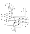
- the mobile phone according to the second embodiment has a configuration as shown in FIG. 4, wherein a power regulation unit 88 is provided in a power amplification circuit within a transmission circuit 14 for regulating an output level of an medium power output to be outputted through a line from the first amplification FET 21 to the second output terminal 52, by regulating a gate voltage of the first amplification FET 21.
- this power regulation unit 88 has a first regulation FET 85 the source of which is grounded through a voltage dividing resistor 83 (R3) and likewise a second regulation FET 86 the source of which is grounded through a voltage dividing resistor 84 (R4).
- a gate of the first regulation FET 85 is connected to a first control terminal 41 (ctl 1) which is connected to the gate of the first switching FET 31, and a gate of the second regulation FET 86 is connected to a second control terminal 42 (ctl 2) which is connected to the gate of the second switching FET 32.
- respective drains of respective regulation FETs 85, 86 are connected through a voltage dividing resistor 81 or a voltage dividing resistor 82 to a reference voltage supply terminal 87 to which a reference voltage (Vdd) is supplied. And, by connecting the gate of the first amplification FET 21 to a node between the voltage dividing resistor 81 and the drain of the first regulation FET 85 as well as to a node between the voltage dividing resistor 82 and the drain of the second regulation FET 86, the power regulation unit 88 is constructed.
- the first regulation FET 85 and the second regulation FET 86 are also fabricated using the aforementioned JP-HEMT, and this power amplification circuit is also formed on one chip.
- the control unit 5 supplies a voltage, for example, of 2.7 V to the first control terminal 41, and a voltage of 0 V to the second control terminal 42.
- the first switching FET 31 is turned ON and the second switching FET 32 is turned OFF as described above, so that a transmission signal supplied through an input terminal 23 is amplified in the first amplification FET 21 and the second amplification FET 22 to a large transmission power, for example, of approximately 28 dBm then to be outputted from the first output terminal 51.
- the first control terminal 41 is supplied, for example, with a voltage of 2.7 V
- the second control terminal 42 is supplied with a voltage of 0 V
- the first regulation FET 85 in the power regulation unit 88 is turned ON-state
- the second regulation FET 86 therein is turned OFF-state.
- the control unit 5 supplies a voltage, for example, of 2.7 V to the second control terminal 42 and a voltage of 0 V to the first control terminal 41.
- the first switching FET 31 is made OFF and the second switching FET 32 is made ON as described above, causing for a transmission signal supplied through the input terminal 23 to be amplified only in the first amplification FET 21 and outputted through the second output terminal 52.
- the second control terminal 42 is supplied a voltage, for example, of 2.7 V and the first control terminal is supplied a voltage of 0 V
- the first regulation FET 85 of the power regulation unit 88 is set OFF
- the second regulation FET 86 is set ON.
- the gate of the first amplification FET 21 there is supplied a voltage with a value obtained by dividing the reference voltage supplied through the reference voltage supply terminal 87 by the voltage dividing resistors 81, 82 and 84.
- the mobile phone according to the second embodiment of the invention is provided with the power regulation unit 88 capable of enhancing the value of voltage to be supplied to the gate of the first amplification FET 21 when the transmission signal is to be amplified only in the first amplification FET 21 before outputting as an medium power output, thereby enabling to improve the value of power of the transmission signal during the outputting of the medium power.
- the mobile phone according to the third embodiment features a phase adjusting circuit provided in the power amplification circuit of the transmitter circuit 14 for canceling a phase difference between a transmission signal to be outputted through the first output terminal 51 and a transmission signal to be outputted through the second output terminal 52.
- the apparatus of the third embodiment differs from the preceding embodiments described above only in this respect. Therefore, only this difference will be described in the following description, omitting duplication of description.
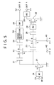
- phase adjusting circuit which is provided in the power amplification circuit of the mobile phone according to the first embodiment.
- a phase adjusting circuit 90 is provided in the line connecting from the first amplification FET 21 to the second output terminal 52.
- phase adjusting circuit 90 is inserted for connection between the DC-cut capacitor 28 which is connected to the drain of the second switching FET 32 and the fourth matching circuit 33 (M4).
- phase adjusting circuit 90 will be described as provided on the side of the line connecting from the first amplification FET 21 to the second output terminal 52, it is not limited thereto, and it may be provided on the side of the line connecting from the first amplification FET 21 to the first output terminal 51 to the same effect.
- this power amplification circuit when outputting a large power, a transmission signal is amplified in a total of two amplification FETs of the first amplification FET 21 and the second amplification FET 22. In contrast, when outputting a medium power, a transmission signal is amplified only in the first amplification FET 21 before its outputting. The transmission signal is rotated of its phase, for example, by 180 degrees through a single amplification FET.
- the phase adjusting circuit 90 cancels this phase difference before outputting the transmission signal. That is, at the time of outputting a medium power, it rotates the phase of a transmission signal from the first amplification FET 21 by 180 degrees before outputting the same.
- phase adjusting circuit 90 is provided in the line for use of outputting a medium power connecting between the first amplification FET 21 and the second output terminal 52, there results in no output loss in a transmission signal to be outputted from the line for use of outputting the high power (i.e., the line connecting between the first amplification FET 21 and the first output terminal 51), thereby enabling for a transmission signal amplified to a high power to be outputted as it is without a loss.
- phase adjusting circuit 90 when the phase adjusting circuit 90 is provided, there occurs a loss in its output more or less. Because it is preferable for the power which is amplified to a large power to be outputted as it is at the time of outputting the large power, in this example, the phase adjusting circuit 90 is installed in the line for use of outputting the medium power.
- phase adjusting circuit 90 may well be installed in the line for use of outputting the large power connecting between the first amplification FET 21 and the first output terminal 51 as described above.
- the mobile phone of the present invention has been set forth as applicable to the mobile phone of the W-CDMA method, however, it is not limited thereto, and it can be applied also to a mobile phone based on other methods such as the PDC method and the like, or to a communication terminal apparatus.
- the present invention has been described as applied to the selection switch for switching between the plural outputs from the power amplification circuit, it is not limited thereto, and it can be applied to any other switching circuit for switching between its outputs, for example, an antenna switch circuit and the like as well.
Landscapes
- Engineering & Computer Science (AREA)
- Power Engineering (AREA)
- Architecture (AREA)
- Mechanical Engineering (AREA)
- Civil Engineering (AREA)
- Structural Engineering (AREA)
- Amplifiers (AREA)
- Semiconductor Integrated Circuits (AREA)
- Junction Field-Effect Transistors (AREA)
- Electronic Switches (AREA)
- Transmitters (AREA)
Applications Claiming Priority (2)
| Application Number | Priority Date | Filing Date | Title |
|---|---|---|---|
| JP2004043589 | 2004-02-19 | ||
| JP2004043589A JP4137815B2 (ja) | 2004-02-19 | 2004-02-19 | 電力増幅装置及び携帯通信端末装置 |
Publications (2)
| Publication Number | Publication Date |
|---|---|
| EP1566886A2 true EP1566886A2 (de) | 2005-08-24 |
| EP1566886A3 EP1566886A3 (de) | 2006-08-09 |
Family
ID=34709128
Family Applications (1)
| Application Number | Title | Priority Date | Filing Date |
|---|---|---|---|
| EP05250943A Withdrawn EP1566886A3 (de) | 2004-02-19 | 2005-02-18 | Leistungsverstärker und Mobilkommunikationsendgerät |
Country Status (5)
| Country | Link |
|---|---|
| US (1) | US7224221B2 (de) |
| EP (1) | EP1566886A3 (de) |
| JP (1) | JP4137815B2 (de) |
| KR (1) | KR101075820B1 (de) |
| CN (1) | CN100468964C (de) |
Families Citing this family (8)
| Publication number | Priority date | Publication date | Assignee | Title |
|---|---|---|---|---|
| US7634290B2 (en) * | 2005-05-31 | 2009-12-15 | Vixs Systems, Inc. | Adjusting transmit power of a wireless communication device |
| JP2007329350A (ja) * | 2006-06-08 | 2007-12-20 | Matsushita Electric Ind Co Ltd | 半導体装置 |
| JP4836253B2 (ja) * | 2006-09-01 | 2011-12-14 | ソニー・エリクソン・モバイルコミュニケーションズ株式会社 | 電力増幅装置および携帯電話端末 |
| JP2010081383A (ja) * | 2008-09-26 | 2010-04-08 | Panasonic Corp | 高周波回路、高周波電力増幅装置、及び半導体装置 |
| CN101867347B (zh) * | 2009-04-15 | 2012-12-12 | 中国科学院电子学研究所 | 多频段无线移动通信系统中频带可重构的功率放大器电路 |
| JP2013048212A (ja) * | 2011-07-28 | 2013-03-07 | Sony Corp | 半導体装置および半導体装置の製造方法 |
| JP2013197599A (ja) | 2012-03-15 | 2013-09-30 | Mitsubishi Electric Corp | 電力増幅器 |
| JP2017183839A (ja) * | 2016-03-28 | 2017-10-05 | 株式会社村田製作所 | 電力増幅回路 |
Family Cites Families (14)
| Publication number | Priority date | Publication date | Assignee | Title |
|---|---|---|---|---|
| US5530923A (en) * | 1994-03-30 | 1996-06-25 | Nokia Mobile Phones Ltd. | Dual mode transmission system with switched linear amplifier |
| US5661434A (en) * | 1995-05-12 | 1997-08-26 | Fujitsu Compound Semiconductor, Inc. | High efficiency multiple power level amplifier circuit |
| CN1081850C (zh) * | 1995-09-29 | 2002-03-27 | 松下电器产业株式会社 | 功率放大器和通信单元 |
| JPH09148852A (ja) * | 1995-11-24 | 1997-06-06 | Matsushita Electric Ind Co Ltd | 送信出力可変装置 |
| US5774017A (en) * | 1996-06-03 | 1998-06-30 | Anadigics, Inc. | Multiple-band amplifier |
| US5973557A (en) * | 1996-10-18 | 1999-10-26 | Matsushita Electric Industrial Co., Ltd. | High efficiency linear power amplifier of plural frequency bands and high efficiency power amplifier |
| US6127886A (en) * | 1997-10-30 | 2000-10-03 | The Whitaker Corporation | Switched amplifying device |
| WO1999043083A1 (en) | 1998-02-19 | 1999-08-26 | Ntt Mobile Communications Network Inc. | Amplifier for radio transmission |
| JP2001111450A (ja) * | 1999-10-13 | 2001-04-20 | Nec Corp | 無線通信装置及びそれに用いる送受信制御方式 |
| JP3600115B2 (ja) * | 2000-04-05 | 2004-12-08 | 株式会社東芝 | 高周波回路及び通信システム |
| US6606483B1 (en) * | 2000-10-10 | 2003-08-12 | Motorola, Inc. | Dual open and closed loop linear transmitter |
| WO2002049209A1 (en) * | 2000-12-15 | 2002-06-20 | Matsushita Electric Industrial Co., Ltd. | Power amplifier and communication apparatus |
| US7071776B2 (en) * | 2001-10-22 | 2006-07-04 | Kyocera Wireless Corp. | Systems and methods for controlling output power in a communication device |
| JP3705431B2 (ja) * | 2002-03-28 | 2005-10-12 | ユーディナデバイス株式会社 | 半導体装置及びその製造方法 |
-
2004
- 2004-02-19 JP JP2004043589A patent/JP4137815B2/ja not_active Expired - Fee Related
-
2005
- 2005-02-07 US US11/050,729 patent/US7224221B2/en not_active Expired - Fee Related
- 2005-02-16 KR KR1020050012809A patent/KR101075820B1/ko not_active Expired - Fee Related
- 2005-02-18 CN CNB200510009312XA patent/CN100468964C/zh not_active Expired - Fee Related
- 2005-02-18 EP EP05250943A patent/EP1566886A3/de not_active Withdrawn
Also Published As
| Publication number | Publication date |
|---|---|
| JP4137815B2 (ja) | 2008-08-20 |
| US20050189989A1 (en) | 2005-09-01 |
| EP1566886A3 (de) | 2006-08-09 |
| CN100468964C (zh) | 2009-03-11 |
| CN1658496A (zh) | 2005-08-24 |
| KR20060042003A (ko) | 2006-05-12 |
| US7224221B2 (en) | 2007-05-29 |
| JP2005236692A (ja) | 2005-09-02 |
| KR101075820B1 (ko) | 2011-10-25 |
Similar Documents
| Publication | Publication Date | Title |
|---|---|---|
| JP3173460B2 (ja) | 電力増幅器 | |
| US7642859B2 (en) | Power amplifier | |
| US6433639B1 (en) | High frequency power amplifier module and wireless communication system | |
| US7298600B2 (en) | Semiconductor integrated circuit device | |
| US6297694B1 (en) | High frequency power amplifier | |
| US7400863B2 (en) | Switch apparatus, switchable power amplification apparatus, and mobile communication terminal apparatus using the same | |
| US7224221B2 (en) | Power amplification apparatus, and mobile communication terminal apparatus | |
| JP5375307B2 (ja) | 半導体装置 | |
| US20030218500A1 (en) | Power amplifier capable of switching gain while suppressing noise power in reception band | |
| US20050233721A1 (en) | Receiver | |
| US7551027B2 (en) | RF power amplifier mirror circuit for sensing current | |
| JP3158776B2 (ja) | 通信機 | |
| US7792506B1 (en) | Power-control circuit with threshold limiting characteristics | |
| Glass et al. | Application of enhancement mode FET technology for wireless subscriber transmit/receive circuits | |
| US7869774B1 (en) | RF saturation voltage sensor | |
| US7912432B1 (en) | Output power detection circuit with threshold limiting characteristics | |
| JP2003037448A (ja) | 高周波電力増幅器 | |
| Choumei et al. | A high efficiency, 2 V single-supply voltage operation RF front-end MMIC for 1.9 GHz Personal Handy Phone Systems | |
| JP2006262518A (ja) | 高周波電力増幅モジュール及び無線通信装置 | |
| Chang et al. | A 1.2-V operation power pseudomorphic high electron mobility transistor for personal handy phone handset application |
Legal Events
| Date | Code | Title | Description |
|---|---|---|---|
| PUAI | Public reference made under article 153(3) epc to a published international application that has entered the european phase |
Free format text: ORIGINAL CODE: 0009012 |
|
| AK | Designated contracting states |
Kind code of ref document: A2 Designated state(s): AT BE BG CH CY CZ DE DK EE ES FI FR GB GR HU IE IS IT LI LT LU MC NL PL PT RO SE SI SK TR |
|
| AX | Request for extension of the european patent |
Extension state: AL BA HR LV MK YU |
|
| PUAL | Search report despatched |
Free format text: ORIGINAL CODE: 0009013 |
|
| AK | Designated contracting states |
Kind code of ref document: A3 Designated state(s): AT BE BG CH CY CZ DE DK EE ES FI FR GB GR HU IE IS IT LI LT LU MC NL PL PT RO SE SI SK TR |
|
| AX | Request for extension of the european patent |
Extension state: AL BA HR LV MK YU |
|
| 17P | Request for examination filed |
Effective date: 20070122 |
|
| 17Q | First examination report despatched |
Effective date: 20070315 |
|
| AKX | Designation fees paid |
Designated state(s): DE FR GB |
|
| RAP1 | Party data changed (applicant data changed or rights of an application transferred) |
Owner name: SONY CORPORATION Owner name: SONY MOBILE COMMUNICATIONS JAPAN, INC. |
|
| GRAP | Despatch of communication of intention to grant a patent |
Free format text: ORIGINAL CODE: EPIDOSNIGR1 |
|
| INTG | Intention to grant announced |
Effective date: 20150210 |
|
| RIN1 | Information on inventor provided before grant (corrected) |
Inventor name: KUSUNOKI, SHIGEO Inventor name: SHIMADA, MASAYUKI Inventor name: KOBAYASHI, TOMOO |
|
| STAA | Information on the status of an ep patent application or granted ep patent |
Free format text: STATUS: THE APPLICATION IS DEEMED TO BE WITHDRAWN |
|
| 18D | Application deemed to be withdrawn |
Effective date: 20150623 |