EP1565803B1 - Circuit de synchronisation avec l'horloge - Google Patents
Circuit de synchronisation avec l'horloge Download PDFInfo
- Publication number
- EP1565803B1 EP1565803B1 EP03775357A EP03775357A EP1565803B1 EP 1565803 B1 EP1565803 B1 EP 1565803B1 EP 03775357 A EP03775357 A EP 03775357A EP 03775357 A EP03775357 A EP 03775357A EP 1565803 B1 EP1565803 B1 EP 1565803B1
- Authority
- EP
- European Patent Office
- Prior art keywords
- signal
- clock
- clock signal
- edge
- circuit
- Prior art date
- Legal status (The legal status is an assumption and is not a legal conclusion. Google has not performed a legal analysis and makes no representation as to the accuracy of the status listed.)
- Expired - Lifetime
Links
- 238000012546 transfer Methods 0.000 claims description 44
- 238000005070 sampling Methods 0.000 claims description 26
- 230000001960 triggered effect Effects 0.000 claims description 22
- 238000003708 edge detection Methods 0.000 claims description 19
- 230000000630 rising effect Effects 0.000 claims description 7
- 230000001934 delay Effects 0.000 claims description 6
- 230000003139 buffering effect Effects 0.000 claims 1
- 230000006870 function Effects 0.000 description 44
- 238000013461 design Methods 0.000 description 5
- 230000004044 response Effects 0.000 description 5
- 238000010586 diagram Methods 0.000 description 3
- 230000005540 biological transmission Effects 0.000 description 2
- 230000003111 delayed effect Effects 0.000 description 2
- 238000000034 method Methods 0.000 description 2
- 238000013459 approach Methods 0.000 description 1
- 230000000903 blocking effect Effects 0.000 description 1
- 238000010276 construction Methods 0.000 description 1
- 230000002596 correlated effect Effects 0.000 description 1
- 230000000875 corresponding effect Effects 0.000 description 1
- 238000005516 engineering process Methods 0.000 description 1
- 230000007257 malfunction Effects 0.000 description 1
- 230000010355 oscillation Effects 0.000 description 1
- 238000012545 processing Methods 0.000 description 1
- 230000001360 synchronised effect Effects 0.000 description 1
Images



Classifications
-
- H—ELECTRICITY
- H04—ELECTRIC COMMUNICATION TECHNIQUE
- H04L—TRANSMISSION OF DIGITAL INFORMATION, e.g. TELEGRAPHIC COMMUNICATION
- H04L7/00—Arrangements for synchronising receiver with transmitter
- H04L7/0008—Synchronisation information channels, e.g. clock distribution lines
- H04L7/0012—Synchronisation information channels, e.g. clock distribution lines by comparing receiver clock with transmitter clock
-
- H—ELECTRICITY
- H04—ELECTRIC COMMUNICATION TECHNIQUE
- H04L—TRANSMISSION OF DIGITAL INFORMATION, e.g. TELEGRAPHIC COMMUNICATION
- H04L7/00—Arrangements for synchronising receiver with transmitter
- H04L7/0008—Synchronisation information channels, e.g. clock distribution lines
-
- H—ELECTRICITY
- H04—ELECTRIC COMMUNICATION TECHNIQUE
- H04L—TRANSMISSION OF DIGITAL INFORMATION, e.g. TELEGRAPHIC COMMUNICATION
- H04L7/00—Arrangements for synchronising receiver with transmitter
- H04L7/0016—Arrangements for synchronising receiver with transmitter correction of synchronization errors
- H04L7/0045—Correction by a latch cascade
Definitions
- the invention relates to a clock synchronization circuit for synchronizing two clock signals for the data transfer between function blocks of different time domains.
- different functional blocks are provided in digital circuits that operate in different time domains and exchange data with each other.
- the different function blocks are clocked by clock signals with different clock frequencies. If the logic function blocks are time-referenced with different clock signals, it must be ensured that data signals transmitted from one function block to the other function block are not misinterpreted.
- the provision of different, uncorrelated time domains on a chip can have different reasons.
- the signal distribution of the clock signal over the entire chip is not possible in many applications, since the clock frequency is too high.
- the random phase difference between the different clock signals may have a high variability compared to the frequency.
- Another possibility is that the clock signal is generated from an external data stream.
- the data signals transmitted between functional blocks of different time domains can not be scanned by conventional registers because the set-up time of the register can be violated by the received data signal, placing the register in a so-called metastable state.
- the phase difference between the two time domains is unknown. The reason for this can either be that the variance of the signal is too large or the inaccuracy of the result value is too high.
- a metastable register generates an illegal data output because the output voltage remains in a mid-range between the supply voltage and the ground voltage. This inadmissible output value can lead to inadmissible data values for further gates and thus to a malfunction of further devices on the entire chip.
- Such synchronizers consist essentially of two cascaded, edge-triggered flip-flops.
- a single-stage synchronizing register has in any case too high a mean error rate MTBF (meantime between failures).
- MTBF mean error rate
- a synchronizing register with two cascaded, edge-triggered flip-flops can be used, since the average error time MTBF can be considered sufficient.
- two cascaded, edge-triggered flip-flops may be used to achieve a sufficiently high average error time MTBF.
- the more independent synchronizing registers are provided, the lower the common mean Error time MTBF.
- the provision of such synchronizing registers is a constant source of uncertainty in the circuit design.
- Fig. 1 shows an example of data transfer by means of queues.
- a FIFO register is used to pass data between function blocks of different time domains.
- the FIFO register includes many memory registers R i .
- the FIFO register is clocked by a first clock signal ⁇ 1 and a second clock signal ⁇ 2 .
- the data is written into the FIFO register at the clock frequency of the first clock signal ⁇ 1 and read out from the FIFO register at the clock frequency of the second clock signal ⁇ 2 .
- the written data comes in the illustrated example of different data channels K i , which are selected by a channel control by means of a multiplexer.
- the channel controller further drives a demultiplexer on the output side of the FIFO register for further data transmission via different data channels K i .
- a full display flag indicates to a function block in the first time domain that the FIFO register is full, and an empty display flag indicates to a function block in the second time domain that the FIFO register is empty.
- head-of-line blocking may occur.
- the queue is blocked by a channel if the corresponding output channel is not ready.
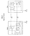
- Fig. 2 shows the principle of a handshake implementation between two functional blocks with synchronous logic operating in different time domains.
- the so-called master is clocked with a first clock signal ⁇ 1
- a slave unit is clocked with a second clock signal ⁇ 2 .
- the clock frequencies of the two clock signals are different.
- the master circuit unit sends a request signal (request) to the slave unit.
- the slave unit detects the request signal (request) and performs the request. Thereafter, the slave unit indicates execution of the task of the master unit by sending an acknowledgment signal back to the master unit.
- the master unit and the slave unit have no common time base, ie they are clocked by clock signals with different clock frequencies, it is essential to ensure that the data signals transmitted between the master unit and the master Slave unit exchanged, due to metastable states not be misinterpreted.
- the reconstructed second clock signal ( ⁇ 2 ') activates a first edge-triggered flip-flop of a data transfer latch, clocked by a first clock signal ( ⁇ 1 ), for latching data output from the first function block.
- the first edge-triggered flip-flop is followed by a second edge-triggered flip-flop of the data transfer buffer which is clocked by the second clock signal ( ⁇ 2 ) and outputs the buffered data to the second function block.
- the logic circuit of the clock synchronization circuit preferably emits either the samples (S) or the edge detection values (E) as a reconstructed second clock signal ( ⁇ 2 ') as a function of an operating mode control signal.
- the signal delay circuit preferably delays the reconstructed second clock signal ( ⁇ 2 ') with a time delay ( ⁇ ) that is a multiple of (N) the clock cycle (T1) of the first clock signal ( ⁇ 1 ), where the multiplication factor (N) is a time delay transfer function edge-to-early signal (ETE) and edge-to-late signal (ETL).
- ⁇ time delay transfer function edge-to-early signal
- ETL edge-to-late signal
- the time delay transfer function is preferably stored in a transfer function logic of the signal delay circuit.
- the transfer function logic preferably controls a multiplexer for switching one of the outputs of a chain of delay elements as an enable signal to the logic circuit.
- the delay elements are preferably clocked by the first clock signal ( ⁇ 1 ).
- the transfer function logic of the signal delay circuit is programmable in a preferred embodiment of the inventive clock synchronization circuit.
- the sampling unit of the clock synchronization circuit preferably contains a first register consisting of two series-connected edge-triggered flip-flops for sampling the second clock signal ( ⁇ 2 ) with the rising signal edge of the first clock signal ( ⁇ 1 ) and a second register consisting of two series-connected, edge-triggered flip-flops for sampling the second clock signal ( ⁇ 2 ) with the falling signal edge of the first clock signal ( ⁇ 1 ), wherein the first register and the second register are connected in parallel for receiving the second clock signal ( ⁇ 2 ) from the second functional block, and a signal edge detector clocked by the first clock signal ( ⁇ 1 ), which outputs an edge detection value to the logic circuit in response to the output sample of the first register and the output sample of the second register and of the sample output in the previous clock cycle.
- the reconstructed second clock signal ( ⁇ 2 ') is output as an indication signal at the second function block, wherein the indication signal indicates that in the Data Transfer Latch Data for reading by the second function block are cached.
- an interface circuit 1 for data transfer between a first functional block 2 and a second functional block 3 is interconnected.
- the interface circuit 1 is used for data transfer between the two function blocks 2, 3, which operate in different time domains.
- the function blocks 2, 3 are any, synchronously operating data processing circuits, which are each clocked with a clock signal.
- the two clock signals ⁇ 1 , ⁇ 2 are uncorrelated or have a variable correlation.
- the first functional block 2 is replaced by the first clock signal ⁇ 1 with a higher clock frequency f ⁇ 1 clocked via a clock line 4.
- the second functional block 3 is supplied via a clock line 5 with the second clock signal ⁇ 2 .
- the second clock signal ⁇ 2 has a lower clock frequency f ⁇ 2 on as the first clock signal ⁇ 1 .
- the data transfer interface circuit 1 ensures the data transfer from the first functional block 2 to the second functional block 3, without metastable data states and thus data errors occurring.
- the data transfer interface circuit 1 contains a data transfer memory 6, which comprises two series-connected, edge-triggered flip-flops 7, 8.
- the data input 9 of the first edge-triggered flip-flop 7 is connected via a data line 10 to a data output 11 of the first function block 2.
- the flip-flop 7 has a data output 11 which is connected via an internal data line 12 of the data transfer buffer 6 to a data input 13 of the second edge-triggered flip-flop 8.
- the second edge-triggered flip-flop 8 also has a data output 14, which outputs buffered data via a data line 15 to a data input 16 of the second function block 3.
- the two flip-flops 7, 8 contained in the data transfer buffer 6 each have a clock input 17, 18.
- the clock input 17 of the first flip-flop 7 is connected to an inverter circuit 19 whose input is connected to the output of an AND gate 20.
- the AND gate 20 combines the line signal 21 supplied via a first clock signal ⁇ 1 with a write enable signal WE, which is output via a line 22 from a signal output 23 of the clock synchronization circuit 24 according to the invention.
- the clock synchronization circuit 24 has two clock signal inputs 25, 26.
- the first clock signal input 25 receives the first clock signal ⁇ 1 , with which the first function block 2 (first time domain) is clocked.
- the second clock signal input 26 of the clock synchronization circuit 24 is supplied with the second clock signal ⁇ 2 , which clocks the second function block 3.
- the clock synchronization circuit 24 has a reset input 27 for receiving a reset signal.
- the clock synchronization circuit 24 serves to synchronize the two clock signals ⁇ 1 , ⁇ 2 .
- the clock synchronization circuit 24 generates a reconstructed second clock signal ⁇ 2 'in the time frame of the first clock signal ⁇ 1 and outputs this via the line 22 as write-enable signal WE to the first flip-flop 7 within the data transfer latch 6 from.
- the reconstructed second clock signal ⁇ 2 is also output via a display signal line 28 to the second functional block 3. This display signal indicates to the function block 3 that data for readout is available in the data transfer buffer 6.
- the clock synchronization circuit 24 receives, via another signal input 29, an operation mode control signal for switching between two modes of operation.
- FIG. 4 shows the circuit design of the clock synchronization circuit 24 according to the invention, as shown in FIG.
- the clock synchronization circuit 24 comprises a sampling unit 30 for sampling the second clock signal ⁇ 2 by the first clock signal ⁇ 1 , the sampling unit 30 generating samples S and edge detection values E of the sampled second clock signal ⁇ 2 .
- the sampling unit receives the second clock signal ⁇ 2 via a signal input 31, which is connected to the input 26 via a line 32.
- the sampling unit 30 includes a clock signal input 33 which receives the applied first clock signal ⁇ 1 via an internal clock signal line 34.
- the sampling unit 30 has two outputs 35, 36. Via the first output 35 it outputs the samples S via a line 37 to a downstream logic circuit 38.
- the detected edge detection values E of the sampled second clock signal ⁇ 2 are also output to the logic circuit 38 via a line 39.
- the logic circuit 38 in turn has a clock signal input 40, which receives the first clock signal ⁇ 1 for clocking the logic circuit 38 via an internal clock line 41.
- the logic circuit 38 has an output 42 which is connected via a line 43 to the signal output 23 of the clock synchronization circuit 24.
- the logic circuit 38 generates a so-called edge-to-early signal ETE when the edge detection value E emitted by the scanning unit 30 assumes a logically high value before an enable signal. Otherwise, the logic circuit 38 generates an edge-too-late signal ETL when the enable signal is received by the logic circuit 38 before the edge detection value E is logic high.
- the enable signal originates from a clock signal delay circuit 44 within the clock synchronization circuit 24.
- the logic circuit 38 outputs the edge-too-early signal ETE via a line 45 and the edge-too-late signal ETL via a line 46 to the clock signal delay circuit 44.
- the clock signal delay circuit 44 has a signal input 47, which via a line 48 to the output 42 of the logic circuit 38 is connected.
- the clock signal delay circuit 44 has an output 49 which applies the enable signal to an input 51 of the logic circuit 38 via a line 50.
- the clock signal delay circuit 44 has a clock signal input 52, which receives the first clock signal ⁇ 1 via an internal clock line 53.
- the clock delay circuit 44 also has two inputs 54, 55 for receiving the edge-to-early signal ETE and for receiving the edge-too-late signal ETL, which are output from the logic circuit 38 via the outputs 56, 57.
- the logic circuit 38 also includes a signal input 58 for receiving the operating mode control signal via a line 59.
- FIG. 5 shows a timing diagram of the two clock signals ⁇ 1 , ⁇ 2 applied to the clock synchronization circuit 24 and the reconstructed second clock signal ⁇ 2 'generated by the clock synchronization circuit 24.
- the clock synchronization circuit 24 maps the rising signal edges of the second low-frequency clock signal ⁇ 2 in the time frame of the first higher-frequency clock signal ⁇ 1 .
- the output reconstructed second clock signal ⁇ 2 ' is reset in order to be able to detect the next rising edge of the second clock signal ⁇ 2 .
- the clock synchronization circuit 24 reconstructs the second clock signal ⁇ 2 in the time frame of the first clock signal ⁇ 1 using a feedback loop.
- the clock delay circuit 44 In the feedback loop is the clock delay circuit 44, which delays the clock signal ⁇ 2 'applied to its signal input 47 by a predetermined number of clock cycles of the first clock signal ⁇ 1 to output at the output 49 at the time when the subsequent phase of the slower second one Clock signal ⁇ 2 is expected.
- the time delay is set by the clock delay circuit 44 in response to the edge-to-early signal ETE and the edge-to-late signal ETL.
- the two of the logic circuit 38 received signals ETE and ETL contain the information as to whether the time delay caused by the clock delay circuit 44 is too long or too short.
- the circuit construction of the clock signal delay circuit 44 will be explained in detail in connection with FIG.
- FIG. 6a shows a preferred embodiment of the sampling unit 30 included in the inventive clock synchronization circuit 24.
- the sampling unit 30 is used to sample the second clock signal ⁇ 2 by the first clock signal ⁇ 1 to generate samples S and edge detection values E of the sampled second clock signal ⁇ 2 .
- the sampling unit 30 has a first clock signal input 33 for the first clock signal and a clock signal input 31 for the second slower clock signal ⁇ 2 .
- the scanning unit has a reset input 60.
- the sampling unit 30 includes a first register 61 and a second register 62.
- the first register 61 comprises two series-connected, edge-triggered flip-flops 61a, 61b.
- the second register 62 comprises two series-connected, edge-triggered flip-flops 62a, 62b.
- the first register 61a is for sampling the second clock signal ⁇ 2 with the rising signal edge of the first clock signal ⁇ 1 .
- the second register 62 is used to sample the second clock signal ⁇ 2 with the falling signal edge of the first clock signal ⁇ 1 .
- the two registers 61, 62 are connected in parallel to receive the second clock signal ⁇ 2 via an internal line 63 of the scanning unit 30.
- the two registers 61, 62 can be reset via the reset input 60.
- the scanning unit 30 includes a clocked signal edge detector 64.
- the signal edge detector 64 includes logic 65, whose truth table is shown in Fig. 6b.
- the signal edge detector 64 includes a delay element 66.
- the sample S output from the second register 62 is output via the output 35 of the sampling unit 30 to the logic circuit 38.
- the sample S is supplied to the signal edge detector 64 and delayed by the delay element 66 by one clock cycle of the first clock signal ⁇ 1 .
- the delay element 66 is preferably an edge-triggered flip-flop, which is clocked with the first clock signal ⁇ 1 .
- the signal edge detector 64 outputs an edge detection value E according to the truth table shown in Fig. 6b in response to the sample S of the second register 62 and the sample S 'of the first register 61 and the sample output at the output 35 in the previous clock cycle.
- Fig. 7 shows a preferred embodiment of the clock signal delay circuit 44.
- the clock signal delay circuit 44 delays the reconstructed second clock signal ⁇ 2 'applied to the output 23 with a time delay ⁇ which is a multiple of the clock cycle T1 of the first clock signal ⁇ 1 .
- the multiplication factor N is set as a function of the edge-to-early signal ETE and the edge-too-late signal ETL.
- the signal delay circuit 44 comprises a chain of M delay elements 67-i, the outputs of which are each connected via lines 68 to inputs 69 of a multiplexer 70.
- the delay elements 67 of the chain each have clock inputs 71 for applying the first clock signal ⁇ 1 via an internal clock line 72.
- the signal delay circuit 44 outputs an enable signal to the logic circuit 38 via its output 49.
- the output 49 of the signal delay circuit 44 is connected via an internal line 73 to the output of the multiplexer 70.
- the multiplexer 70 switches one of its inputs 69i to the enable signal output 49 in response to a control signal received via a control line 74.
- the control signal is received by the multiplexer 70 via the control signal line 74 from a transfer function logic contained in the signal delay circuit 44 75.
- the transfer function logic 75 receives via lines 76, 77 the edge-to-early signal ETE and the edge-to-late signal ETL from the logic circuit 38.
- the transfer function logic 75 may be hardwired or, in a preferred embodiment, a stored transfer function contain. In this case, the transfer function logic 75 can be programmed via programming lines 78.
- the transfer function indicates whether the time delay due to the signal delay by the signal delay circuit 44 is too long or too short.
- the transfer function is a discrete function. It can lead to an oscillation between two state values, which lie next to an optimum value. For example, if the optimum time delay is 4.5 clock cycles, the transfer function will produce alternate time delays of four or five clock cycles of the high frequency first clock signal.
- the transfer function can be set or programmed independently of the other circuits on the chip.
- ETE K , ETL K indicate the value of ETE, ETL at the nth clock cycle of the high-frequency first clock signal ⁇ 1 , then:
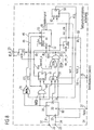
- Fig. 8 shows a particularly preferred embodiment of the inventive clock synchronization circuit 24.
- the logic circuit 38 a special circuit design.
- the logic circuit 38 in this preferred embodiment comprises a NOR gate 79, an AND gate 80, a set-reset flip-flop 81, a multiplexer 82, a logic 83, a latch flip-flop 84, a latch latch -Flop 85 and a set-reset flip-flop 86.
- the timing of the flip-flops 81, 84, 85, 86 of the logic circuit 38 is effected by the first clock signal ⁇ 1 .
- the set input takes precedence.
- the reset input takes precedence.
- the logic circuit 38 can be switched between two operating modes.
- the samples S are output as a reconstructed second clock signal ⁇ 2 '
- the edge detection values E are output from the clock synchronization circuit 24 as a reconstructed second clock signal.
- the multiplexer 82 is followed by the logic circuit 83, which comprises an inverter 83a, an OR gate 83b and an AND gate 83c.
- the sample sampling mode is activated if the frequency of the first clock signal is about the same as the clock frequency of the second clock signal. In this case, the scanning unit 30 detects most of the signal edges. In the theoretical case that the two clock frequencies are identical, the scanning unit 30 would detect no signal edge and recognize a constant value. With increasing frequency difference between the two clock frequencies of the clock signals ⁇ 1 , ⁇ 2 , the sampling unit comprises more and more signal edges.
- the edge operation mode ie when the detected edge detection values E are output as a reconstructed second clock signal ⁇ 2 ', if the delay is too short, the next signal edge is waited before a new external clock signal period is considered to be started.
- the next high logic value is waited for, and if the transfer function causes too short a signal delay, a high logical value belonging to the same logic high external clock signal phase can be detected and taken into account as a new phase when the clock synchronization circuit according to the invention causes an adjustable signal delay by means of the signal delay circuit 44 to replica of the to form the slower clock signal ⁇ 2 in the time frame of the faster clock signal ⁇ 1 .
- the clock synchronization circuit according to the invention has the advantage that it contains no analog components. Furthermore, since it does not comprise any special components, the digital logic circuit 38 can be synthesized in a simple manner, ie can be written on with standard cells from a component library. The circuit design of the clock synchronization circuit 24 according to the invention is low. By means of the clock synchronization circuit according to the invention, the interface 1 between the function blocks 2, 3 operate at a very high data throughput rate.
Landscapes
- Engineering & Computer Science (AREA)
- Computer Networks & Wireless Communication (AREA)
- Signal Processing (AREA)
- Synchronisation In Digital Transmission Systems (AREA)
- Manipulation Of Pulses (AREA)
- Logic Circuits (AREA)
- Information Transfer Systems (AREA)
Claims (10)
- Circuit de synchronisation d'horloge pour la synchronisation d'un premier signal d'horloge (Φ1) et d'un deuxième signal d'horloge (Φ2) pour le transfert de données d'un premier bloc fonctionnel (2), cadencé à une fréquence d'horloge (fΦ1) plus élevée par le premier signal d'horloge (Φ1), vers un deuxième bloc fonctionnel (3), cadencé à une fréquence d'horloge (fΦ2) plus basse par le deuxième signal d'horloge (Φ2), le circuit de synchronisation d'horloge (24) comprenant :(a) une unité de balayage (30) pour le balayage du deuxième signal d'horloge (Φ2) par le premier signal d'horloge (Φ1) pour la génération de valeurs d'échantillonnage (S) et de valeurs de détection de flanc (E) du deuxième signal d'horloge (Φ2) balayé, et caractérisé par :(b) un circuit logique (38), cadencé avec le premier signal d'horloge (Φ1), qui délivre à une sortie (42) du circuit logique (38), en fonction d'un signal de commande - mode de fonctionnement, les valeurs d'échantillonnage (S) générées ou les valeurs de détection de flanc (E) générées comme deuxième signal d'horloge reconstruit (Φ2') dans la zone temporelle du premier signal d'horloge (Φ1), la sortie (42) du circuit logique (38) étant réinitialisée après la sortie d'une valeur (S, E) jusqu'à ce que le circuit logique (38) reçoive un signal de validation,
le circuit logique (38) générant un signal Edge-too-Early (ETE) lorsque la valeur de détection de flanc (E) générée avant la réception du signal de validation est logiquement élevée et un signal Edge-too-Late (ETL) lorsque le signal de validation est reçu avant que la valeur de détection de flanc (E) générée soit logiquement élevée,(c) et un circuit de retard de signal (44), cadencé avec le premier signal d'horloge (Φ1), qui retarde le deuxième signal d'horloge (Φ2') reconstruit délivré par le circuit logique (38) avec un délai temporel (τ) variable en fonction du signal Edge-too-Early (ETE) et du signal Edge-too-Late (ETL) pour la génération du signal de validation. - Circuit de synchronisation d'horloge selon la revendication 1, caractérisé en ce que,
le deuxième signal d'horloge (Φ2') reconstruit active un premier flip-flop (7) d'une mémoire temporaire de transfert de données (6) pour la mémorisation temporaire de données issues du premier bloc fonctionnel (2), le flip-flop (7) étant déclenché par flanc et cadencé par le premier signal d'horloge (Φ1). - Circuit de synchronisation d'horloge selon la revendication 2, caractérisé en ce que,
un deuxième flip-flop (8) de la mémoire temporaire de transfert de données (6), déclenché par flanc, cadencé par le deuxième signal d'horloge (Φ2), est connecté en aval du premier flip-flop (7) déclenché par flanc, il délivre les données mémorisées temporairement au deuxième bloc fonctionnel (3). - Circuit de synchronisation d'horloge selon la revendication 1, caractérisé en ce que,
le circuit de retard de signal (44) retarde le deuxième signal d'horloge (Φ2') reconstruit avec un délai temporel (τ) qui est un multiple du cycle d'horloge (Ti) du premier signal d'horloge (Φ1), le facteur de multiplication étant une fonction de transfert de délai temporel du signal Edge-Too-Early (ETE) et du signal Edge-Too-Late (ETL). - Circuit de synchronisation d'horloge selon la revendication 4, caractérisé en ce que,
la fonction de transfert de délai temporel est mémorisée dans une logique fonctionnelle de transfert (75) du circuit de retard de signal (44). - Circuit de synchronisation d'horloge selon la revendication 5, caractérisé en ce que,
la logique fonctionnelle de transfert (75) commande un multiplexeur (70) pour commuter une des sorties d'une chaîne (67) d'éléments de retard (67-i) comme signal de validation pour le circuit logique (38). - Circuit de synchronisation d'horloge selon la revendication 6, caractérisé en ce que,
les éléments de retard (67-i) sont cadencés par le premier signal d'horloge (Φ1). - Circuit de synchronisation d'horloge selon la revendication 5, caractérisé en ce que,
la logique fonctionnelle de transfert (75) du circuit de retard de signal (44) est programmable. - Circuit de synchronisation d'horloge selon la revendication 1, caractérisé en ce que,
l'unité de balayage (30) comprend :un premier registre (61), pour le balayage du deuxième signal d'horloge (Φ2) avec le flanc de signal montant du premier signal d'horloge (Φ1), qui comprend deux flip-flops (61a, 61b) connectés en série et déclenchés par flanc,un deuxième registre (62), pour le balayage du deuxième signal d'horloge (Φ2) avec le flanc de signal descendant du premier signal d'horloge (Φ1), qui
comprend deux flip-flops (62a, 62b) connectés en série et déclenchés par flanc,le premier registre (61) et le deuxième registre (62) étant connectés en parallèle pour la réception du deuxième signal d'horloge (Φ2), etun détecteur de flanc de signaux (64), cadencé par le premier signal d'horloge (Φ1), qui délivre une valeur de détection de flanc (E) au circuit logique (38) en fonction de la valeur d'échantillonnage délivrée du premier registre (61), de la valeur d'échantillonnage délivrée du deuxième registre (62) et de la valeur d'échantillonnage du deuxième registre, sortie dans le cycle d'horloge préalable. - Circuit de synchronisation d'horloge selon la revendication 1, caractérisé en ce que,
le deuxième signal d'horloge (Φ2') reconstruit est délivré comme signal d'indication au deuxième bloc fonctionnel (3), le signal d'indication indiquant que des données pour l'extraction par le deuxième bloc fonctionnel (3) sont mémorisées temporairement dans la mémoire temporaire de transfert de données (6).
Applications Claiming Priority (3)
| Application Number | Priority Date | Filing Date | Title |
|---|---|---|---|
| DE10255685 | 2002-11-28 | ||
| DE10255685A DE10255685B3 (de) | 2002-11-28 | 2002-11-28 | Taktsynchronisationsschaltung |
| PCT/EP2003/012747 WO2004049140A2 (fr) | 2002-11-28 | 2003-11-14 | Circuit de synchronisation avec l'horloge |
Publications (2)
| Publication Number | Publication Date |
|---|---|
| EP1565803A2 EP1565803A2 (fr) | 2005-08-24 |
| EP1565803B1 true EP1565803B1 (fr) | 2006-03-22 |
Family
ID=32335838
Family Applications (1)
| Application Number | Title | Priority Date | Filing Date |
|---|---|---|---|
| EP03775357A Expired - Lifetime EP1565803B1 (fr) | 2002-11-28 | 2003-11-14 | Circuit de synchronisation avec l'horloge |
Country Status (6)
| Country | Link |
|---|---|
| US (1) | US7180332B2 (fr) |
| EP (1) | EP1565803B1 (fr) |
| JP (1) | JP4091941B2 (fr) |
| CN (1) | CN1717643A (fr) |
| DE (2) | DE10255685B3 (fr) |
| WO (1) | WO2004049140A2 (fr) |
Families Citing this family (25)
| Publication number | Priority date | Publication date | Assignee | Title |
|---|---|---|---|---|
| US7515668B1 (en) * | 2005-01-26 | 2009-04-07 | Xilinx, Inc. | Data and/or clock recovery circuits with sampling offset correction |
| US7577039B2 (en) * | 2005-11-16 | 2009-08-18 | Montage Technology Group, Ltd. | Memory interface to bridge memory buses |
| US7558124B2 (en) * | 2005-11-16 | 2009-07-07 | Montage Technology Group, Ltd | Memory interface to bridge memory buses |
| US7368950B2 (en) * | 2005-11-16 | 2008-05-06 | Montage Technology Group Limited | High speed transceiver with low power consumption |
| US7969819B2 (en) * | 2006-05-09 | 2011-06-28 | Schlumberger Technology Corporation | Method for taking time-synchronized seismic measurements |
| US7593273B2 (en) * | 2006-11-06 | 2009-09-22 | Altera Corporation | Read-leveling implementations for DDR3 applications on an FPGA |
| CN101662354B (zh) * | 2008-08-29 | 2012-05-02 | 盛群半导体股份有限公司 | 用于usb传输即时声音数据的同步装置 |
| US8013764B1 (en) * | 2009-01-31 | 2011-09-06 | Xilinx, Inc. | Method and apparatus for shifting the bits of a wide data word |
| US8555104B2 (en) * | 2010-01-13 | 2013-10-08 | Broadcom Corporation | Frequency adapter utilized in high-speed internal buses |
| US8396563B2 (en) * | 2010-01-29 | 2013-03-12 | Medtronic, Inc. | Clock synchronization in an implantable medical device system |
| JP5431290B2 (ja) * | 2010-10-29 | 2014-03-05 | インターナショナル・ビジネス・マシーンズ・コーポレーション | クロック・ドメイン・クロッシングのデータ転送回路および方法 |
| CN102480289A (zh) * | 2010-11-25 | 2012-05-30 | 上海华虹集成电路有限责任公司 | 一种同步异频时钟对齐的设计电路 |
| GB2497525A (en) | 2011-12-12 | 2013-06-19 | St Microelectronics Ltd | Controlling shared memory data flow |
| US8897324B2 (en) * | 2012-02-01 | 2014-11-25 | Microchip Technology Incorporated | Timebase peripheral |
| GB2503474B (en) * | 2012-06-27 | 2016-06-29 | Nordic Semiconductor Asa | Data transfer between clock domains |
| US9164134B2 (en) | 2012-11-13 | 2015-10-20 | Nvidia Corporation | High-resolution phase detector |
| US9471091B2 (en) * | 2012-11-28 | 2016-10-18 | Nvidia Corporation | Periodic synchronizer using a reduced timing margin to generate a speculative synchronized output signal that is either validated or recalled |
| US9438256B2 (en) * | 2014-06-03 | 2016-09-06 | Apple Inc. | Slow to fast clock synchronization |
| US9680459B2 (en) | 2014-12-11 | 2017-06-13 | Intel Corporation | Edge-aware synchronization of a data signal |
| CN104535918B (zh) * | 2014-12-22 | 2017-03-15 | 中国民航大学 | 一种跨时钟域同步器内部常数测试电路和方法 |
| CN106155180A (zh) * | 2015-03-23 | 2016-11-23 | 惠州市德赛西威汽车电子股份有限公司 | 一种车载嵌入式的异步多时钟处理方法 |
| US9864399B2 (en) * | 2015-12-10 | 2018-01-09 | Apple Inc. | Timebase synchronization |
| CN109488287B (zh) * | 2018-11-01 | 2022-07-22 | 中国石油集团长城钻探工程有限公司 | 一种中子和密度仪数据同步方法 |
| CN112104435B (zh) * | 2020-08-28 | 2022-08-30 | 新华三技术有限公司 | 一种时钟延时补偿方法、逻辑装置及网络设备 |
| JP7706334B2 (ja) * | 2021-10-25 | 2025-07-11 | 株式会社デンソー | クロック信号生成回路 |
Family Cites Families (17)
| Publication number | Priority date | Publication date | Assignee | Title |
|---|---|---|---|---|
| ES2100159T3 (es) * | 1990-12-18 | 1997-06-16 | Alcatel Bell Nv | Circuito de sincronismo. |
| US5256912A (en) * | 1991-12-19 | 1993-10-26 | Sun Microsystems, Inc. | Synchronizer apparatus for system having at least two clock domains |
| US5604884A (en) * | 1993-03-22 | 1997-02-18 | Compaq Computer Corporation | Burst SRAMS for use with a high speed clock |
| US5584007A (en) * | 1994-02-09 | 1996-12-10 | Ballard Synergy Corporation | Apparatus and method for discriminating among data to be stored in cache |
| US5548620A (en) * | 1994-04-20 | 1996-08-20 | Sun Microsystems, Inc. | Zero latency synchronized method and apparatus for system having at least two clock domains |
| US5638015A (en) * | 1995-06-21 | 1997-06-10 | Unisys Corporation | Avoiding instability |
| US5654988A (en) * | 1995-09-29 | 1997-08-05 | Intel Corporation | Apparatus for generating a pulse clock signal for a multiple-stage synchronizer |
| US5905766A (en) * | 1996-03-29 | 1999-05-18 | Fore Systems, Inc. | Synchronizer, method and system for transferring data |
| US6219395B1 (en) * | 1997-09-16 | 2001-04-17 | Natural Microsystems, Corp. | Phase alignment of frames in computer telephony busses |
| US6000022A (en) * | 1997-10-10 | 1999-12-07 | Micron Technology, Inc. | Method and apparatus for coupling signals between two circuits operating in different clock domains |
| JP3560793B2 (ja) * | 1997-11-27 | 2004-09-02 | 株式会社東芝 | データ転送方法 |
| US6359479B1 (en) * | 1998-08-04 | 2002-03-19 | Juniper Networks, Inc. | Synchronizing data transfers between two distinct clock domains |
| EP1113353A2 (fr) | 1999-12-16 | 2001-07-04 | Texas Instruments Incorporated | Appareil et procédé de capture efficace de signaux produits dans un domaine d'horloge rapide par un circuit dans un domain d'horloge lent |
| DE60006812D1 (de) | 2000-04-17 | 2004-01-08 | Italtel Spa | Schaltung zur synchronisation von impulsen, die im jeweils anderen geltungsbereich zweier verschiedener taktsignale erzeugt werden |
| US6327207B1 (en) | 2001-04-09 | 2001-12-04 | Lsi Logic Corporation | Synchronizing data operations across a synchronization boundary between different clock domains using two-hot encoding |
| US6988215B2 (en) * | 2001-09-14 | 2006-01-17 | Medtronic, Inc. | Method and apparatus for synchronization of clock domains |
| US6744285B2 (en) * | 2002-08-08 | 2004-06-01 | Agilent Technologies, Inc. | Method and apparatus for synchronously transferring data across multiple clock domains |
-
2002
- 2002-11-28 DE DE10255685A patent/DE10255685B3/de not_active Expired - Fee Related
-
2003
- 2003-11-14 WO PCT/EP2003/012747 patent/WO2004049140A2/fr not_active Ceased
- 2003-11-14 CN CNA2003801043714A patent/CN1717643A/zh active Pending
- 2003-11-14 US US10/536,282 patent/US7180332B2/en not_active Expired - Lifetime
- 2003-11-14 DE DE50302759T patent/DE50302759D1/de not_active Expired - Lifetime
- 2003-11-14 EP EP03775357A patent/EP1565803B1/fr not_active Expired - Lifetime
- 2003-11-14 JP JP2004554349A patent/JP4091941B2/ja not_active Expired - Fee Related
Also Published As
| Publication number | Publication date |
|---|---|
| CN1717643A (zh) | 2006-01-04 |
| WO2004049140A3 (fr) | 2004-12-02 |
| WO2004049140A2 (fr) | 2004-06-10 |
| US7180332B2 (en) | 2007-02-20 |
| DE50302759D1 (de) | 2006-05-11 |
| EP1565803A2 (fr) | 2005-08-24 |
| JP2006508438A (ja) | 2006-03-09 |
| DE10255685B3 (de) | 2004-07-29 |
| US20060140317A1 (en) | 2006-06-29 |
| JP4091941B2 (ja) | 2008-05-28 |
Similar Documents
| Publication | Publication Date | Title |
|---|---|---|
| EP1565803B1 (fr) | Circuit de synchronisation avec l'horloge | |
| DE3687956T2 (de) | Datensynchronisator zwischen einer sende- und einer empfangsanlage. | |
| DE10102887B4 (de) | Verzögerungsvorrichtung, die eine Verzögerungssperrschleife aufweist und Verfahren zum Kalibrieren derselben | |
| DE68923834T2 (de) | Leistungsfähiges Protokoll für die Übertragung zwischen asynchronen Vorrichtungen. | |
| DE69615471T2 (de) | Verfahren und Vorrichtung zur dynamischen Berechnung von Füllungsgraden eines synchronen Fifo-Puffer | |
| EP3907886B1 (fr) | Appareil de synchronisation de données dans des systèmes ayant de multiples domaines d'horloge et de réinitialisation | |
| DE60202856T2 (de) | Methode und system zur automatischen verzögerungserkennung und empfängeranpassung für eine synchrone busschnittstelle | |
| DE69332401T2 (de) | Verbesserte ein- und mehrstufige FIFO-Entwürfe für Datenübertragungssynchronisiereinrichtungen | |
| US8386828B1 (en) | Circuit for estimating latency through a FIFO buffer | |
| DE19914986A1 (de) | Vorrichtung zum Verzögern eines Taktsignals | |
| US7609092B2 (en) | Automatic phase-detection circuit for clocks with known ratios | |
| CN109240981B (zh) | 多通道数据的同步采集方法、设备和计算机可读存储介质 | |
| DE102013221678A1 (de) | System und Verfahren zum Bestimmen einer Zeit zum sicheren Abtasten eines Signals einer Takt-Domäne | |
| DE102016122763A1 (de) | Zugreifen auf daten über verschiedene takte | |
| DE69031639T2 (de) | Synchronisiereinrichtung, welche Taktphasenextrapolation verwendet | |
| EP0471207B1 (fr) | Dispositif pour la régénération et synchronisation d'un signal numérique | |
| DE10345150B3 (de) | Verfahren, Vorrichtung und System zum Analysieren digitaler Schaltungen | |
| DE60015939T2 (de) | Verfahren und schaltung um an zwei enden getakten daten zu empfangen | |
| US5790891A (en) | Synchronizing unit having two registers serially connected to one clocked elements and a latch unit for alternately activating the registers in accordance to clock signals | |
| US5561691A (en) | Apparatus and method for data communication between two asynchronous buses | |
| DE10122702C2 (de) | Verfahren und Vorrichtung zum Erzeugen eines zweiten Signals mit einem auf einem zweiten Takt basierenden Takt aus einem ersten Signal mit einem ersten Takt | |
| DE19811591C2 (de) | Taktsignal modellierende Schaltung mit negativer Verzögerung | |
| AT512192B1 (de) | Synchrone sequentielle logikvorrichtung mit doppelt getriggerten flipflops sowie eine methode zum gezielt zeitversetzten triggern solcher zustandspeichernden register | |
| DE10333522B4 (de) | Speicheranordnung zur Verarbeitung von Daten und Verfahren | |
| US6999542B1 (en) | Data ready indicator between different clock domains |
Legal Events
| Date | Code | Title | Description |
|---|---|---|---|
| PUAI | Public reference made under article 153(3) epc to a published international application that has entered the european phase |
Free format text: ORIGINAL CODE: 0009012 |
|
| 17P | Request for examination filed |
Effective date: 20050504 |
|
| AK | Designated contracting states |
Kind code of ref document: A2 Designated state(s): AT BE BG CH CY CZ DE DK EE ES FI FR GB GR HU IE IT LI LU MC NL PT RO SE SI SK TR |
|
| GRAP | Despatch of communication of intention to grant a patent |
Free format text: ORIGINAL CODE: EPIDOSNIGR1 |
|
| RBV | Designated contracting states (corrected) |
Designated state(s): DE FR GB |
|
| GRAS | Grant fee paid |
Free format text: ORIGINAL CODE: EPIDOSNIGR3 |
|
| GRAA | (expected) grant |
Free format text: ORIGINAL CODE: 0009210 |
|
| AK | Designated contracting states |
Kind code of ref document: B1 Designated state(s): DE FR GB |
|
| REG | Reference to a national code |
Ref country code: GB Ref legal event code: FG4D Free format text: NOT ENGLISH |
|
| REF | Corresponds to: |
Ref document number: 50302759 Country of ref document: DE Date of ref document: 20060511 Kind code of ref document: P |
|
| GBT | Gb: translation of ep patent filed (gb section 77(6)(a)/1977) |
Effective date: 20060517 |
|
| ET | Fr: translation filed | ||
| PLBE | No opposition filed within time limit |
Free format text: ORIGINAL CODE: 0009261 |
|
| STAA | Information on the status of an ep patent application or granted ep patent |
Free format text: STATUS: NO OPPOSITION FILED WITHIN TIME LIMIT |
|
| 26N | No opposition filed |
Effective date: 20061227 |
|
| REG | Reference to a national code |
Ref country code: FR Ref legal event code: PLFP Year of fee payment: 13 |
|
| REG | Reference to a national code |
Ref country code: FR Ref legal event code: PLFP Year of fee payment: 14 |
|
| REG | Reference to a national code |
Ref country code: FR Ref legal event code: PLFP Year of fee payment: 15 |
|
| PGFP | Annual fee paid to national office [announced via postgrant information from national office to epo] |
Ref country code: GB Payment date: 20181120 Year of fee payment: 16 Ref country code: FR Payment date: 20181123 Year of fee payment: 16 |
|
| PGFP | Annual fee paid to national office [announced via postgrant information from national office to epo] |
Ref country code: DE Payment date: 20190121 Year of fee payment: 16 |
|
| REG | Reference to a national code |
Ref country code: DE Ref legal event code: R119 Ref document number: 50302759 Country of ref document: DE |
|
| GBPC | Gb: european patent ceased through non-payment of renewal fee |
Effective date: 20191114 |
|
| PG25 | Lapsed in a contracting state [announced via postgrant information from national office to epo] |
Ref country code: GB Free format text: LAPSE BECAUSE OF NON-PAYMENT OF DUE FEES Effective date: 20191114 Ref country code: DE Free format text: LAPSE BECAUSE OF NON-PAYMENT OF DUE FEES Effective date: 20200603 Ref country code: FR Free format text: LAPSE BECAUSE OF NON-PAYMENT OF DUE FEES Effective date: 20191130 |