EP1560235B1 - Composant multicouche électrique - Google Patents
Composant multicouche électrique Download PDFInfo
- Publication number
- EP1560235B1 EP1560235B1 EP20050001704 EP05001704A EP1560235B1 EP 1560235 B1 EP1560235 B1 EP 1560235B1 EP 20050001704 EP20050001704 EP 20050001704 EP 05001704 A EP05001704 A EP 05001704A EP 1560235 B1 EP1560235 B1 EP 1560235B1
- Authority
- EP
- European Patent Office
- Prior art keywords
- layers
- electrode
- electrode layers
- layer
- shielding
- Prior art date
- Legal status (The legal status is an assumption and is not a legal conclusion. Google has not performed a legal analysis and makes no representation as to the accuracy of the status listed.)
- Not-in-force
Links
- 239000003990 capacitor Substances 0.000 claims description 105
- 239000000463 material Substances 0.000 claims description 19
- KDLHZDBZIXYQEI-UHFFFAOYSA-N Palladium Chemical compound [Pd] KDLHZDBZIXYQEI-UHFFFAOYSA-N 0.000 claims description 6
- BASFCYQUMIYNBI-UHFFFAOYSA-N platinum Chemical compound [Pt] BASFCYQUMIYNBI-UHFFFAOYSA-N 0.000 claims description 6
- PXHVJJICTQNCMI-UHFFFAOYSA-N Nickel Chemical compound [Ni] PXHVJJICTQNCMI-UHFFFAOYSA-N 0.000 claims description 4
- 230000001419 dependent effect Effects 0.000 claims description 4
- BQCADISMDOOEFD-UHFFFAOYSA-N Silver Chemical compound [Ag] BQCADISMDOOEFD-UHFFFAOYSA-N 0.000 claims description 3
- 229910052709 silver Inorganic materials 0.000 claims description 3
- 239000004332 silver Substances 0.000 claims description 3
- RYGMFSIKBFXOCR-UHFFFAOYSA-N Copper Chemical compound [Cu] RYGMFSIKBFXOCR-UHFFFAOYSA-N 0.000 claims description 2
- 229910001252 Pd alloy Inorganic materials 0.000 claims description 2
- 229910001260 Pt alloy Inorganic materials 0.000 claims description 2
- 229910052802 copper Inorganic materials 0.000 claims description 2
- 239000010949 copper Substances 0.000 claims description 2
- 229910052759 nickel Inorganic materials 0.000 claims description 2
- 229910052763 palladium Inorganic materials 0.000 claims description 2
- 229910052697 platinum Inorganic materials 0.000 claims description 2
- 229910001316 Ag alloy Inorganic materials 0.000 claims 2
- 239000000919 ceramic Substances 0.000 description 19
- 238000010586 diagram Methods 0.000 description 11
- 230000008878 coupling Effects 0.000 description 5
- 238000010168 coupling process Methods 0.000 description 5
- 238000005859 coupling reaction Methods 0.000 description 5
- 230000015572 biosynthetic process Effects 0.000 description 3
- 238000006073 displacement reaction Methods 0.000 description 3
- 229910002113 barium titanate Inorganic materials 0.000 description 2
- JRPBQTZRNDNNOP-UHFFFAOYSA-N barium titanate Chemical compound [Ba+2].[Ba+2].[O-][Ti]([O-])([O-])[O-] JRPBQTZRNDNNOP-UHFFFAOYSA-N 0.000 description 2
- 229910010293 ceramic material Inorganic materials 0.000 description 2
- 238000005516 engineering process Methods 0.000 description 2
- 238000004519 manufacturing process Methods 0.000 description 2
- 238000007639 printing Methods 0.000 description 2
- 238000005245 sintering Methods 0.000 description 2
- 239000006228 supernatant Substances 0.000 description 2
- 230000001629 suppression Effects 0.000 description 2
- 208000032365 Electromagnetic interference Diseases 0.000 description 1
- 229910052772 Samarium Inorganic materials 0.000 description 1
- RTAQQCXQSZGOHL-UHFFFAOYSA-N Titanium Chemical compound [Ti] RTAQQCXQSZGOHL-UHFFFAOYSA-N 0.000 description 1
- IHWJXGQYRBHUIF-UHFFFAOYSA-N [Ag].[Pt] Chemical compound [Ag].[Pt] IHWJXGQYRBHUIF-UHFFFAOYSA-N 0.000 description 1
- 229910052788 barium Inorganic materials 0.000 description 1
- YIMPFANPVKETMG-UHFFFAOYSA-N barium zirconium Chemical compound [Zr].[Ba] YIMPFANPVKETMG-UHFFFAOYSA-N 0.000 description 1
- 230000000694 effects Effects 0.000 description 1
- 230000005684 electric field Effects 0.000 description 1
- 230000005686 electrostatic field Effects 0.000 description 1
- 230000010354 integration Effects 0.000 description 1
- 229910052751 metal Inorganic materials 0.000 description 1
- 239000002184 metal Substances 0.000 description 1
- 238000000034 method Methods 0.000 description 1
- 238000012986 modification Methods 0.000 description 1
- 230000004048 modification Effects 0.000 description 1
- 230000007935 neutral effect Effects 0.000 description 1
- SWELZOZIOHGSPA-UHFFFAOYSA-N palladium silver Chemical compound [Pd].[Ag] SWELZOZIOHGSPA-UHFFFAOYSA-N 0.000 description 1
- 230000001681 protective effect Effects 0.000 description 1
- 238000007650 screen-printing Methods 0.000 description 1
- 238000005476 soldering Methods 0.000 description 1
- 230000003068 static effect Effects 0.000 description 1
Images


Classifications
-
- H—ELECTRICITY
- H01—ELECTRIC ELEMENTS
- H01G—CAPACITORS; CAPACITORS, RECTIFIERS, DETECTORS, SWITCHING DEVICES, LIGHT-SENSITIVE OR TEMPERATURE-SENSITIVE DEVICES OF THE ELECTROLYTIC TYPE
- H01G4/00—Fixed capacitors; Processes of their manufacture
- H01G4/30—Stacked capacitors
-
- H—ELECTRICITY
- H01—ELECTRIC ELEMENTS
- H01G—CAPACITORS; CAPACITORS, RECTIFIERS, DETECTORS, SWITCHING DEVICES, LIGHT-SENSITIVE OR TEMPERATURE-SENSITIVE DEVICES OF THE ELECTROLYTIC TYPE
- H01G4/00—Fixed capacitors; Processes of their manufacture
- H01G4/002—Details
- H01G4/005—Electrodes
-
- H—ELECTRICITY
- H01—ELECTRIC ELEMENTS
- H01G—CAPACITORS; CAPACITORS, RECTIFIERS, DETECTORS, SWITCHING DEVICES, LIGHT-SENSITIVE OR TEMPERATURE-SENSITIVE DEVICES OF THE ELECTROLYTIC TYPE
- H01G4/00—Fixed capacitors; Processes of their manufacture
- H01G4/002—Details
- H01G4/005—Electrodes
- H01G4/012—Form of non-self-supporting electrodes
Definitions
- the invention relates to an electrical multilayer component with electrode layers and dielectric layers.
- a multilayer electrical component which has a main body and with stacked electrode layers of a first and a second type separated by dielectric layers and which form at least one capacitance.
- the electrode layers are contacted on the side surfaces of the base body to the outside.
- the publication JP 2000 228329 A discloses a capacitor array having a plurality of multilayer capacitors, wherein the multilayer capacitors are each formed of opposing internal electrodes and intervening dielectric layers. Shielding electrodes for suppressing stray capacitances are respectively arranged between adjacent multilayer capacitors.
- the present invention makes use of the basic principle, according to which, in the case of an electroceramic multilayer component, a plurality of capacitors can be integrated into a single basic body.
- the individual capacitances are formed by opposing electrode layers, between which a dielectric layer is arranged.
- Scattering capacitances may occur between adjacent capacitors, which are undesirable.
- the stray capacitances result, on the one hand, from the local proximity of the electrode layers forming the capacitors.
- An increased distance of the two electrode layers results in an improved decoupling, whereby stray capacitances can be reduced.
- Multilayer electrical components are produced according to the present invention by providing a plurality of dielectric layers, for example green sheets, then printing on these green sheets with a metal-containing paste, the printed area later forming the electrode layer. If a green film is then coated with a plurality of electrode layers, then the electrode layers lie in one plane in the case of a rectangular design of the multilayer component. However, it is also conceivable not to stack the dielectric layers one above the other and then to sinter them, but to give the electrode layers the dielectric layers of any other external shape. The dielectric layers are, as long as they are still present as a green sheet, very flexible and therefore adaptable to various forms.
- an electrical multilayer component which contains at least two capacitors which are each formed from opposing electrode layers and at least one intervening dielectric layer. At least two electrode layers belonging to different capacitors are laterally offset from each other.
- a component is advantageous in which at least one shielding layer is arranged between two laterally offset electrode layers.
- each of the two mutually offset electrode layers is at least partially or completely overlapped by a shielding layer.
- the lateral displacement of two electrode layers relative to one another in this context means that the displacement of one electrode layer relative to the other electrode layer takes place in the plane of one of the two electrode layers.
- Side-offset electrode layers are obtained, for example, by arranging two such layer stacks side by side and at different heights in the multilayer component.
- a shielding layer may itself be an electrode layer, that is to say that it is part of a capacitor contained in the multilayer component.
- the shielding layer has sufficiently good electroconductive properties, so that it is suitable for shielding electrostatic fields.
- the shielding layer may preferably lie in a plane which is parallel to the staggered electrode layers.
- each of the two electrode layers with a shielding layer, the decoupling between the two layers can be further improved.
- the two electrode layers can be overlapped by one and the same shielding layer.
- the overlap of the two electrode layers, which belong to different capacitors, has the advantage that the component takes up less space with the same capacity.
- two shielding layers are provided between two electrode layers, which overlap one another.
- At least one dielectric layer lies between two shielding layers.
- This embodiment has the advantage that a separate capacitance can be formed by the shielding layers, which on the one hand enables a defined coupling between the shielding layers and on the other hand form an additional capacitor present in the component, which can be connected from the outside and can be used accordingly.
- only one shielding layer is provided between two electrode layers, wherein said one shielding layer overlaps both electrode layers.
- each shielding layer is part of one or more capacitors.
- the shielding layers can take over another function in addition to the decoupling of adjacent electrode layers. Being part of a capacitor, they can contribute to the capacitance of another capacitor integrated in the device.
- the capacitance of the capacitors present in the component can advantageously be increased.
- a first type of electrode layers is provided, which contribute substantially only to a first capacitor.
- a second type of electrode layers is provided, which in turn substantially only one contribute second capacitor.
- the electrode layers of each grade are in the form of layers stacked one above the other. The stacks thus formed are laterally offset from one another.
- the concept of lateral displacement of stacks to each other is to be interpreted as well, as has already been described above.
- At least one shielding layer is disposed between each first-type electrode layer and each second-order electrode layer. These can each be one and the same shielding layer.
- the shielding layer preferably runs parallel to the electrode layers.
- This embodiment of the device extends the concept of decoupling individual electrode layers to all electrode layers belonging to a capacitor. As a result, the decoupling between two capacitors present in the component can be further improved.
- each shielding layer contributes to each of the two capacitors.
- the capacitance of the two capacitors contained in the component can be increased in a simple manner and, above all, in a space-saving manner. Because the increase in capacity happens in this case without the application of additional electrode layers, but only by using the already necessary for decoupling of the capacitors shielding.
- the respectively lowermost electrode layer and the respective uppermost electrode layer of the component are provided with a shielding layer on their upper and lower sides.
- This embodiment has the advantage that the electrode layers are also well shielded from the outside.
- this embodiment may also be advantageous, namely, if the remaining components of the multilayer component are arranged symmetrically, that is, that the electrode layers are arranged so that the component can be mounted both with the bottom and with the top on a circuit board, without a difference.
- the provision of shielding layers at the upper edge and at the lower end of the stacked electrode layers can additionally contribute to the security of rotation of the component.
- two capacitors have the same capacitance.
- the device is designed very homogeneous, that is, that it can also be easily formed against rotation, so that upper and lower sides can be mounted on a printed circuit board with equal rights.
- SMT surface mount technology
- the capacitors provided in the component have different capacities.
- capacitor ceramic With regard to the dielectric layers, it is particularly advantageous if they contain a so-called capacitor ceramic. These capacitor ceramics have particularly advantageous properties, for example with regard to the temperature dependence of the dielectric constant.
- capacitor ceramic for example, a ceramic based on barium titanate into consideration. It is particularly possible to use so-called "C0G” ceramics. Such a material would be, for example, (Sm, Ba) NdCiO 3 ceramics.
- HQM materials come into consideration, which are formed from basic materials which are similar to those of C0G masses.
- a material with voltage-dependent resistance that is to say a so-called varistor ceramic
- systems may be considered as varistor ceramics. containing ZnO-Bi or ZnO-Pr.
- Such dielectric layers have the advantage that, in addition to the capacitor, they integrate a varistor into the multilayer component as a further component.
- ESD Electro Static Discharge
- the component it is advantageous if, for example, silver, palladium, platinum, as well as a silver-palladium alloy, a silver-platinum alloy or else copper or nickel are used as the material for the electrode layers and optionally also for shielding layers , These materials have the advantage that they have good sintering properties in common sintering with many different ceramics.
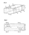
- FIG. 1 shows the main body 6 of a multilayer component in a perspective view.
- the component has a longitudinal axis 7, along which the component extends.
- the main body 6 is cuboid, but may also have any other geometric shape.
- the cuboid shape has the advantage that the component is relatively easy to manufacture and can be used without much additional effort for the SMT (Surface Mount Technology).
- On the side surfaces of the base body 6 outer terminals A 1 , A 2 , A 3 , A 4 are arranged.
- the external connections are applied opposite each other. That is, the outer terminal A 1 is the outer terminal A 4 and the outer terminal A 2 is the outer terminal A 3 opposite.
- the external connections can be made, for example, by burning in a silver stoving paste or other suitable material. They are not only arranged on the side surfaces, but they also surround the base body 6 at its boundary edges and thus cover small parts of the top or the base of the body 6. By this measure, it can be ensured that the device is surface mountable. It can then simply be placed on top or on the bottom of a soldering point and soldered using the Lotddlings the device on a circuit board.
- FIG. 2 showed a longitudinal section through the device FIG. 1 , It can be seen that the base body 6 is formed from superimposed dielectric layers 8. These dielectric layers 8 may be, for example, ceramic green sheets, which are stacked, pressed, cut and then sintered in the deformable state, so that a monolithic base body 6 is formed. On individual dielectric layers 8 electrode layers 21, 22, 31, 32 are applied. These Electrode layers are applied in the production of the main body of the device by printing a screen printing paste or with another suitable method on the still free surface of the respective dielectric layer. Subsequently, the printed dielectric layers are stacked, and further processed as described above ready.
- These dielectric layers 8 may be, for example, ceramic green sheets, which are stacked, pressed, cut and then sintered in the deformable state, so that a monolithic base body 6 is formed.
- electrode layers 21, 22, 31, 32 are applied on individual dielectric layers 8 electrode layers 21, 22, 31, 32 are applied. These Electrode layers are applied in the production of the main body of the device by printing
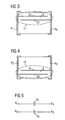
- the electrode layers 21, 22 and 31, 32 disposed in the main body each form a capacitor 11 and 12, respectively.
- the two capacitors are integrated together in the multilayer component. This results in the advantage that less device area is consumed for the realization of two capacitors on a circuit board, as if the capacitors are present in individual multilayer components.
- the electrode layers 21, 22 belonging to the capacitor 11 and the electrode layers 31, 32 belonging to the capacitor 12 are laterally offset from one another.
- This lateral offset has been made in the direction of the longitudinal axis 7 of the component and corresponds to the arrangement of the side of the body 6 arranged on the outside terminals A 1 , A 2 , A 3 , A 4th
- the electrode layers 21, 22 are contacted with the external terminals A 1 and A 4 .
- the electrode layers 31, 32 are contacted with the external terminals A 2 and A 3 . Due to the lateral offset of the Electrode layers 21, 22 and 31, 32 and thus the capacitors 11 and 12 formed thereby, a further electrostatic decoupling of the two capacitors 11, 12 can be achieved, which further reduces the stray capacitance in an advantageous manner.
- FIG. 3 shows a section through the device FIG. 2 along the line III-III.
- the electrode layer 21 is connected to the external terminal A 1 .
- the electrode layer 22 is connected to the external terminal A 4 .
- the electrode layer 21 and the electrode layer 22 overlap one another and thus form a capacitor 11.
- a dielectric layer 8 is arranged between the electrode layers 21, 22.
- the dielectric layers 8 in FIG. 2 all designated by the same reference numeral, this does not mean that these dielectric layers must all consist of the same material. Rather, it is also possible to use 8 different materials for the dielectric layers.
- FIG. 4 shows a section along the line IV-IV FIG. 2 , So through the capacitor 12. Accordingly FIG. 3 It can again be seen that the electrode layer 32 is connected to the external terminal A 2 and the electrode layer 31 to the external terminal A 3 .
- FIG. 5 shows the equivalent circuit for the device FIG. 2 , It can be seen here that in the case of the external connection A 1 and A 4, a capacitor with the capacitance C 1 and between the external connection A 2 and A 3 another capacitor with the capacitance C 2 is switched.
- FIG. 6A shows an embodiment of a device with a shielding layer 41.
- an electrode layer 21 and an electrode layer 31 are provided in the device.
- a 1 , A 3 and A 4 is indicated with which external terminal the respective electrode layer is contacted in each case.
- the external connections are not shown even in the perspective view.
- FIG. 6A nor the dielectric layers 8, which are all designated by the same reference numerals, which may well consist of different materials. This may mean, for example, that the uppermost dielectric layer 8 is made of a different material than the subsequent dielectric layer 8.
- FIG. 6B is in a longitudinal section too FIG. 6A can be seen that the electrode layer 21 forms a first capacitor 11 with the shielding layer 41, which in turn also represents an electrode layer.
- the electrode layer 31 with the shielding layer 41 forms a further capacitor 12.
- the shielding layer 41 is thus part of each of a capacitor 11, 12 and also serves the shielding between the electrode layers 21, 31, since now no more linear connection in geometrical terms between the electrode layers 21, 31 is possible without the Shielding layer 41 to cross. This means that electric fields that would produce a possible coupling between the electrode layer 21 and the electrode layer 31 are effectively shielded by the electrically conductive shielding layer 41. Thereby, the stray capacitance between the capacitors 11 and 12 is effectively reduced.
- the shielding layer 41, the two electrode layers 21, 31 laterally surmounted so a supernatant 9 is provided laterally.
- the shield can be made particularly effective.
- FIG. 6A can be seen that the shielding layer 41 is largely adapted in shape on the one hand to the electrode layer 21 and on the other hand to the shape of the electrode layer 31, so that a maximum overlap surface for forming the respective capacitor 11, 12 is present.
- FIG. 6B there is advantageously an overlap, so that the shielding layer 41 laterally projects beyond the electrode layers 21, 31. This is, however, the FIG. 6A not to be taken.
- FIG. 6C shows an equivalent circuit diagram of the device FIG. 6A .
- the capacitors 11 and 12 therefore have capacitances C 1 and C 2 and are interconnected in such a way that the terminal A 1 is connected to both capacitors and the terminals A 4 and A 3 are connected only to one of the two capacitors. Starting from the external connection A 1 thus results in a star connection.
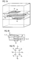
- FIG. 7A shows a further embodiment of the device.
- the shielding layer 41 is not only connected to an external terminal but with two external terminals, namely A 2 and A 4 .
- the electrode layers 21 and 31 have an overlap not only with the opposite shielding layer 41 but also with each other.
- FIG. 7B where it is designated by the reference numeral 10.
- FIG. 7B It can be seen that the electrode layer 21 forms two capacitors 11, 12 with the shielding layer 41. This arises in particular in conjunction with FIG. 7A , Here it can be seen that starting from the outer terminal A 4, a first capacitor is formed over the electrode layer 21, the shielding layer 41 to the outer terminal A 2 and that a second capacitor 12 is formed, starting from the outer terminal A 3 via the electrode layer 21, the shielding 41 to the external connection A 4 .
- This embodiment of the device has the advantage that four capacitors can be provided with three electrode layers.
- FIG. 7D shows an extension of the in FIG. 7A shown component.
- the device according to Figure 7D is designed as a so-called tripod.
- This means that the shielding electrode 41 is connected from one side, from the rear side of the component, to three external terminals.
- the external connections A 4 and A 3 correspond to those in FIG. 1 shown external connections.
- an external terminal A 6 is still shown in FIG. 1 is indicated by dashed lines and which is arranged between the external terminals A 4 and A 3 . From the opposite side, the shielding layer 41 is made accessible by the external connection A 5 .
- the shielding layer 41 is made accessible by the external connection A 5 .
- the electrode layers 21, 31 are contacted from different sides of the component.
- the electrode layers 21, 31 are contacted from the same side of the component, namely with the external terminals A 1 and A 2 .
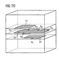
- Figure 7E shows an extension of the embodiment Figure 7D . Similar to the embodiment of Figure 7D are in the example according to Figure 7E additional external connections A 5 and A 6 are provided. These external connections are shown in FIG. 1 by dashed additional external connections A 5 and A 6 .
- Electrode layers 22, 32 are provided which can increase the capacitance of the capacitors.
- the electrode layers 21 and 22 are connected to the external terminal A 4 .
- the electrode layers 31 and 32 are connected to the external terminal A 3 .
- shielding layers 41, 42, 43, 44, 45 are provided which are each contacted on the rear side of the component with three external connections A 1 , A 2 and A 5 .
- the shielding layers 41, 42, 43, 44, 45 are contacted with the external terminal A 6 .
- a shielding layer 41, 42, 43, 44, 45 is arranged to form a capacitor, each having an electrode layer.
- unlike the Figure 9A at the upper end and at the lower end of the layer stack each have a shielding layer 41, 45, which provides the symmetry increase and improve the shielding of the device to the outside.
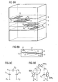
- FIG. 8A shows a further component in a perspective view, wherein two shielding layers are included.
- the two shielding layers 41 and 51 are different in shape in that they are contacted with different external terminals.
- the shielding layer 41 is contacted with the external terminal A 3 and the shielding layer 51 with the external terminal A 1 . Together with the overlap which the two shielding layers 41, 51 have with each other, this results in the formation of a further capacitor, which can be connected from the outside via the external connections A 1 and A 3 .
- the electrode layers 21 and 31, which are contacted with the external terminal A 2 and A 4 respectively.
- the electrode layer 31 forms a further capacitor 13 with the shielding layer 51.
- the two shielding layers 41, 51 together form another capacitor 12.
- this additional capacitor can be connected from the outside.
- the purpose can therefore be achieved, on the one hand, to decouple the two electrode layers 21 and 31 particularly effectively, namely from one another by means of two superimposed shielding layers.
- the two capacitors 11 and 13 receive a defined coupling, which is defined by the capacitance of the capacitor 12.
- a defined coupling is clear in many applications more advantageous than an undefined stray capacitance between two capacitors arranged in a multilayer component.
- the capacitor 12 representing the defined coupling can be used as noise suppression in an interference suppression circuit.
- FIG. 8B is still to be seen that as in Figures 6B and 7B shown, a supernatant of the shielding layers 41, 51 via the respective shielding electrode layer 21, 31 is particularly advantageous.
- FIG. 8C shows a first equivalent circuit diagram for the device Figure 8A in the event that only capacitor materials are used for the dielectric layers 8.
- the equivalent circuit consists of three capacitors with capacitances C 1 , C 2 and C 3 .
- the capacitor 12 represented by the capacitance C 2 is accessible from outside through the external connections A 1 and A 2 and can thus be externally connected.
- FIG. 8C To FIG. 8C is still to say that the three capacitances C 1 , C 2 , C 3 form a ⁇ -circuit.
- FIG. 8D Another diagram variant shows Figure 8D , It is assumed here that at least the dielectric layers 8 lying between two electrode layers or between an electrode layer and a shielding layer or between two shielding layers all contain a varistor material. This results in a parallel connection of a voltage-dependent resistor VDR 1 , VDR 2 and VDR 3 to each capacitor C 1 , C 2 , C 3 .
- VDR 1 , VDR 2 and VDR 3 a voltage-dependent resistor
- VDR 1 , VDR 2 and VDR 3 to each capacitor C 1 , C 2 , C 3 .
- Two electrode layers with an intermediate varistor ceramic thus form on the one hand a capacitor due to the electrode layers and the intervening dielectric, and on the other hand, a varistor due to the voltage-dependent resistance of the intermediate ceramic layer.
- the two components are connected in parallel, as well Figure 8D can be seen.
- Such a device equipped with varistor ceramic has the advantage that it can be used as an EMI filter.
- only one or more other of the dielectric layers 8 can be designed as a varistor material.
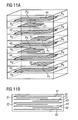
- FIG. 9A shows a further embodiment of a multilayer component according to the in FIG. 6A featured type, with an extension is to see that yet another capacitor is integrated into the device.
- This is achieved by providing three different types of electrode layers, namely electrode layers 21, 22 and 23. These three electrode layers 21, 22, 23 are contacted with different external connections, A 2 for electrode layer 21, A 4 for electrode layer 22 and A 3 for electrode layer 23.
- the three electrode layers 21, 22, 23 are, as well FIG. 9B it can be seen, each involved in the formation of a
- the capacitor 13 is formed by the electrode layer 21 and the overlying shielding layer 41.
- the underlying shielding layer 42 is still involved in the capacitor 13.
- the shielding layers 41, 42, 43 have identical shape and are therefore assigned to the same type of shielding layer. They are all connected to the external connection A 1 .
- the capacitor 12 is formed by the electrode layer 22 as well as by the shielding layer 41 and by the shielding layer 43.
- the capacitor 11 is formed by the electrode layer 23 and the shielding layer 43.
- the shielding layer 43 and the shielding layer 42 are respectively involved in two different capacitors ,
- the shielding layer 43 is involved only in the capacitor 13.
- the electrode layer 21 as the counter electrode for the formation of a capacitor, both the shielding layer 42 and the uppermost shielding layer 41 is available.
- the uppermost shielding layer 41 would not necessarily be required to form a capacitor.
- the capacitance of the capacitor 13 can be increased by it, because once again the same capacity comes to it as the capacitance formed between the electrode layer 21 and the shielding layer 42.
- the shielding layer 41 still has the advantage that the electrode layer 21 is shielded to the outside.
- FIG. 9C shows an equivalent circuit diagram for the device Figure 9A where a star circuit of three capacitances C 1 , C 2 , C 3 can be seen, the external terminal A 1 forms the neutral point.
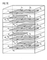
- FIG. 10A shows by way of example how a component formed according to the basic principle of Figure 8A can be extended by adding more layers.
- a further electrode layer 32 is now provided.
- this additional electrode layer 32 which is of the same type as the electrode layer 31, that is, that it has the same shape and that it also has the same horizontal position and that it is also connected to the same external terminal, here A 4 .
- the capacitance of one of the capacitors formed in the component can be increased.
- FIG. 8C shows a further electrode layer 32 to provide good shielding between the electrode layers 31 and 21.
- the shielding layers 41 and 52 again contribute to the capacitor between the external terminals A 1 and A 3 , see also this FIG. 8C , where the capacitor is designated by the capacitance C 2 , contribute.
- the shielding layers 51 and 52 and 53 and 54 in FIG Figure 10A are all of the same type. Likewise, the shielding layers 41 and 42 in Figure 10A of the same type. For the further addition of an electrode layer 31, the addition of the shielding layer 52 would have been sufficient, so that the shielding layers 51 and 54 are not absolutely necessary for this purpose. You can in Figure 10A therefore also be omitted.
- a shielding layer as the uppermost layer in the device may have the advantage that the uppermost electrode layer 31 is well shielded not only against the electrode layer 21 but also outwardly.
- the shielding layer 51 can also compare to the capacitance of the capacitor formed with the electrode layer 31, cf. FIG. 8C the capacity C 1 , contribute.
- the capacitor 11 is formed with the participation of the electrode layer 21 and the shielding layers 41 and 42 that the capacitor 12 is formed with the participation of the shielding layers 53 and 42 and the shielding layers 41 and 52 and that the capacitor 13 is formed the electrode layers 32 and the shielding layers 53 and 54 and the electrode layer 31 and the shielding layers 52 and 51. Otherwise, the following applies to the device Figure 10A the equivalent circuit after FIG. 8C ,
- FIG. 7A shows by example how the basic principle FIG. 7A can be extended by adding more layers.
- Shielding layers 41, 42, 43, 44 and 45 are provided as the shielding layers. All of these shielding layers are of the same type, that is to say they are all connected to the outer terminals A 2 and A 4 and otherwise have the same shape and the same horizontal positioning, that is to say that they are identical with respect to the stacking direction.
- the outer shielding layers 41 and 45 serve to shield the device to the outside.
- the capacitance of each capacitor formed here can be increased.
- the component shown preferably has a footprint smaller than 2.5 mm 2 .
- Particularly advantageous is a footprint of 1.37 mm 2 , which corresponds to the design 0405 and has the advantage that a particularly small component area is required for the two capacitors.
- the elements described here can also be duplicated side by side in a single component, which is the number of Increased capacitors and what can be realized, for example, in the 0508 design.
- Figure 8D shows still the advantage in the integration of varistor materials in the dielectric layers, which is evident from the fact that the varistors VDR 1 , VDR 2 and VDR 3 are already integrated into the multilayer component, which are dispensed with separate varistors with appropriate circuit according to the prior art can.
- the invention is not limited in the number of electrode layers. It has been shown that concepts presented here can be arbitrarily extended in the number of electrode layers.
Landscapes
- Engineering & Computer Science (AREA)
- Power Engineering (AREA)
- Manufacturing & Machinery (AREA)
- Microelectronics & Electronic Packaging (AREA)
- Fixed Capacitors And Capacitor Manufacturing Machines (AREA)
- Ceramic Capacitors (AREA)
Claims (12)
- Composant multicouche électrique- contenant au moins deux condensateurs (11, 12, 13, 14) qui sont respectivement formés de couches d'électrode (21, 41, 51) opposées avec au moins une couche de diélectrique (8) interposée entre elles,- dans lequel au moins une couche de blindage (41, 51) est disposée entre deux couches d'électrode (21, 22, 31, 32) décalées latéralement l'une par rapport à l'autre,- lequel contient une pluralité de couches d'électrode (21, 22) d'une première sorte qui contribuent à un seul premier condensateur (11),- lequel contient une pluralité de couches d'électrode (31, 32) d'une deuxième sorte qui contribuent à un seul deuxième condensateur (12),- dans lequel les deux sortes de couches d'électrode (21, 22, 31, 32) sont présentes à chaque fois en forme d'empilage les unes au-dessus des autres,- dans lequel les piles sont décalées latéralement les unes par rapport aux autres,- dans lequel au moins une couche de blindage (41, 51) est disposée entre chaque couche d'électrode (21, 22) de la première sorte et chaque couche d'électrode (31, 32) de la deuxième sorte,
caractérisé en ce que- les couches d'électrode (21, 22) de la première sorte et les couches d'électrode (31, 32) de la deuxième sorte se chevauchent. - Composant selon la revendication 1, dans lequel chacune des deux couches d'électrode (21, 22, 31, 32) décalées latéralement l'une par rapport à l'autre est au moins partiellement recouverte par une couche de blindage (41, 42, 43, 44, 45, 51, 52, 53, 54).
- Composant selon l'une des revendications 1 ou 2, dans lequel sont prévues deux couches de blindage (41, 42, 43, 44, 45, 51, 52, 53, 54), lesquelles présentent un chevauchement (10) entre elles.
- Composant selon la revendication 2, dans lequel est prévue une couche de blindage (41) qui chevauche les deux couches d'électrode (21, 31).
- Composant selon l'une des revendications 1 à 4, dans lequel chaque couche de blindage (41, 51) fait partie d'un ou plusieurs condensateurs (11, 12, 13, 14).
- Composant selon l'une des revendications 1 à 5, dans lequel chaque couche de blindage (41, 51) contribue à chacun des deux condensateurs (11, 12).
- Composant selon l'une des revendications 2 à 6, dans lequel la couche d'électrode (21, 22, 31, 32) respectivement la plus basse et la couche d'électrode (21, 22, 31, 32) respectivement la plus haute du composant est à chaque fois munie d'une couche de blindage (51, 41) sur le côté supérieur et sur le côté inférieur.
- Composant selon l'une des revendications 1 à 7, dans lequel deux condensateurs (11, 12) possèdent la même capacité (C1, C2).
- Composant selon l'une des revendications 1 à 7, dans lequel deux condensateurs (11, 12) possèdent des capacités (C1, C2) différentes.
- Composant selon l'une des revendications 1 à 9, dans lequel les couches d'électrode (21, 22, 31, 32) contiennent de l'argent, du palladium, du platine, un alliage d'argent et de palladium, un alliage d'argent et de platine, du cuivre ou du nickel.
- Composant selon l'une des revendications 1 à 10, dans lequel les couches de diélectrique (8) contiennent un matériau ayant une résistance dépendante de la tension.
- Composant selon l'une des revendications 1 à 10, dans lequel les couches de diélectrique (8) contiennent un matériau de condensateur.
Applications Claiming Priority (2)
| Application Number | Priority Date | Filing Date | Title |
|---|---|---|---|
| DE200410004096 DE102004004096A1 (de) | 2004-01-27 | 2004-01-27 | Elektrisches Vielschichtbauelement |
| DE102004004096 | 2004-01-27 |
Publications (3)
| Publication Number | Publication Date |
|---|---|
| EP1560235A2 EP1560235A2 (fr) | 2005-08-03 |
| EP1560235A3 EP1560235A3 (fr) | 2008-01-02 |
| EP1560235B1 true EP1560235B1 (fr) | 2012-06-06 |
Family
ID=34638760
Family Applications (1)
| Application Number | Title | Priority Date | Filing Date |
|---|---|---|---|
| EP20050001704 Not-in-force EP1560235B1 (fr) | 2004-01-27 | 2005-01-27 | Composant multicouche électrique |
Country Status (2)
| Country | Link |
|---|---|
| EP (1) | EP1560235B1 (fr) |
| DE (1) | DE102004004096A1 (fr) |
Families Citing this family (3)
| Publication number | Priority date | Publication date | Assignee | Title |
|---|---|---|---|---|
| TWI277988B (en) | 2004-11-18 | 2007-04-01 | Tdk Corp | Multilayer capacitor |
| DE102006013227A1 (de) * | 2005-11-11 | 2007-05-16 | Epcos Ag | Elektrisches Vielschichtbauelement |
| JP7136638B2 (ja) * | 2018-09-11 | 2022-09-13 | 太陽誘電株式会社 | 積層セラミックコンデンサ、その包装体、および部品実装回路基板 |
Family Cites Families (9)
| Publication number | Priority date | Publication date | Assignee | Title |
|---|---|---|---|---|
| JPH0653078A (ja) * | 1992-07-27 | 1994-02-25 | Mitsubishi Materials Corp | バリスタ機能付き積層コンデンサアレイ |
| JPH06151245A (ja) * | 1992-11-06 | 1994-05-31 | Mitsubishi Materials Corp | ノイズフィルタ |
| JP3328399B2 (ja) * | 1993-12-08 | 2002-09-24 | ティーディーケイ株式会社 | 積層コンデンサアレイ |
| JPH07169649A (ja) * | 1993-12-16 | 1995-07-04 | Tdk Corp | 積層貫通型コンデンサアレイ |
| JPH1012490A (ja) * | 1996-06-20 | 1998-01-16 | Murata Mfg Co Ltd | 貫通型積層コンデンサアレイ |
| JP3470566B2 (ja) * | 1997-09-19 | 2003-11-25 | 株式会社村田製作所 | 積層型電子部品 |
| JP2000228329A (ja) * | 1999-02-08 | 2000-08-15 | Matsushita Electric Ind Co Ltd | 多連型積層セラミックコンデンサ |
| DE10064447C2 (de) * | 2000-12-22 | 2003-01-02 | Epcos Ag | Elektrisches Vielschichtbauelement und Entstörschaltung mit dem Bauelement |
| JP2003068568A (ja) * | 2001-08-27 | 2003-03-07 | Matsushita Electric Ind Co Ltd | 積層セラミックコンデンサ |
-
2004
- 2004-01-27 DE DE200410004096 patent/DE102004004096A1/de not_active Ceased
-
2005
- 2005-01-27 EP EP20050001704 patent/EP1560235B1/fr not_active Not-in-force
Also Published As
| Publication number | Publication date |
|---|---|
| EP1560235A2 (fr) | 2005-08-03 |
| DE102004004096A1 (de) | 2005-08-18 |
| EP1560235A3 (fr) | 2008-01-02 |
Similar Documents
| Publication | Publication Date | Title |
|---|---|---|
| EP2174328B1 (fr) | Composant multicouche électrique avec une résistance et une couche de découplage | |
| EP2143117B1 (fr) | Composant électrique multicouche comportant une structure de blindage sans contact électrique | |
| DE4008507C2 (de) | Laminiertes LC-Filter | |
| EP1606831B1 (fr) | Composant multicouche electrique | |
| EP1350257B1 (fr) | Composant multicouche electrique et circuit antiparasites pourvu d'un tel composant | |
| DE19628890A1 (de) | Elektronikteile mit eingebauten Induktoren | |
| EP1369880B1 (fr) | Composant électrique multicouche et circuit | |
| EP1880399B1 (fr) | Element de traversee electrique | |
| EP1425762B1 (fr) | Composant multicouche electrique | |
| EP1369881B1 (fr) | Composant électrique multicouche | |
| EP1560235B1 (fr) | Composant multicouche électrique | |
| DE102004010001A1 (de) | Elektrisches Bauelement und schaltungsanordnung mit dem Bauelement | |
| DE102004016146B4 (de) | Elektrisches Vielschichtbauelement | |
| EP1391898B1 (fr) | Composant électrique multicouche | |
| EP1537655B1 (fr) | Filtre de resonance multiple | |
| DE60036238T2 (de) | Vielschicht-Keramikkondensator für dreidimensionale Montage | |
| DE112020002057T5 (de) | Komponente mit niedriger Induktivität | |
| EP2246866B1 (fr) | Composant électrique et agencement de circuit | |
| DE102004029411B4 (de) | Keramischer Mehrschichtkondensator | |
| WO2003009311A1 (fr) | Composant electroceramique |
Legal Events
| Date | Code | Title | Description |
|---|---|---|---|
| PUAI | Public reference made under article 153(3) epc to a published international application that has entered the european phase |
Free format text: ORIGINAL CODE: 0009012 |
|
| AK | Designated contracting states |
Kind code of ref document: A2 Designated state(s): AT BE BG CH CY CZ DE DK EE ES FI FR GB GR HU IE IS IT LI LT LU MC NL PL PT RO SE SI SK TR |
|
| AX | Request for extension of the european patent |
Extension state: AL BA HR LV MK YU |
|
| PUAL | Search report despatched |
Free format text: ORIGINAL CODE: 0009013 |
|
| AK | Designated contracting states |
Kind code of ref document: A3 Designated state(s): AT BE BG CH CY CZ DE DK EE ES FI FR GB GR HU IE IS IT LI LT LU MC NL PL PT RO SE SI SK TR |
|
| AX | Request for extension of the european patent |
Extension state: AL BA HR LV MK YU |
|
| 17P | Request for examination filed |
Effective date: 20080610 |
|
| AKX | Designation fees paid |
Designated state(s): DE FR GB |
|
| 17Q | First examination report despatched |
Effective date: 20100301 |
|
| REG | Reference to a national code |
Ref country code: DE Ref legal event code: R079 Ref document number: 502005012770 Country of ref document: DE Free format text: PREVIOUS MAIN CLASS: H01G0004380000 Ipc: H01G0004012000 |
|
| GRAP | Despatch of communication of intention to grant a patent |
Free format text: ORIGINAL CODE: EPIDOSNIGR1 |
|
| RIC1 | Information provided on ipc code assigned before grant |
Ipc: H01G 4/012 20060101AFI20111212BHEP Ipc: H01G 4/005 20060101ALI20111212BHEP Ipc: H01G 4/30 20060101ALI20111212BHEP |
|
| GRAS | Grant fee paid |
Free format text: ORIGINAL CODE: EPIDOSNIGR3 |
|
| GRAA | (expected) grant |
Free format text: ORIGINAL CODE: 0009210 |
|
| RIN1 | Information on inventor provided before grant (corrected) |
Inventor name: FEICHTINGER, THOMAS Inventor name: ORTNER, MARKUS |
|
| AK | Designated contracting states |
Kind code of ref document: B1 Designated state(s): DE FR GB |
|
| REG | Reference to a national code |
Ref country code: GB Ref legal event code: FG4D Free format text: NOT ENGLISH |
|
| REG | Reference to a national code |
Ref country code: DE Ref legal event code: R096 Ref document number: 502005012770 Country of ref document: DE Effective date: 20120802 |
|
| PLBE | No opposition filed within time limit |
Free format text: ORIGINAL CODE: 0009261 |
|
| STAA | Information on the status of an ep patent application or granted ep patent |
Free format text: STATUS: NO OPPOSITION FILED WITHIN TIME LIMIT |
|
| 26N | No opposition filed |
Effective date: 20130307 |
|
| REG | Reference to a national code |
Ref country code: DE Ref legal event code: R097 Ref document number: 502005012770 Country of ref document: DE Effective date: 20130307 |
|
| PGFP | Annual fee paid to national office [announced via postgrant information from national office to epo] |
Ref country code: DE Payment date: 20140124 Year of fee payment: 10 |
|
| PGFP | Annual fee paid to national office [announced via postgrant information from national office to epo] |
Ref country code: FR Payment date: 20140124 Year of fee payment: 10 |
|
| PGFP | Annual fee paid to national office [announced via postgrant information from national office to epo] |
Ref country code: GB Payment date: 20140123 Year of fee payment: 10 |
|
| REG | Reference to a national code |
Ref country code: DE Ref legal event code: R119 Ref document number: 502005012770 Country of ref document: DE |
|
| GBPC | Gb: european patent ceased through non-payment of renewal fee |
Effective date: 20150127 |
|
| PG25 | Lapsed in a contracting state [announced via postgrant information from national office to epo] |
Ref country code: GB Free format text: LAPSE BECAUSE OF NON-PAYMENT OF DUE FEES Effective date: 20150127 Ref country code: DE Free format text: LAPSE BECAUSE OF NON-PAYMENT OF DUE FEES Effective date: 20150801 |
|
| REG | Reference to a national code |
Ref country code: FR Ref legal event code: ST Effective date: 20150930 |
|
| PG25 | Lapsed in a contracting state [announced via postgrant information from national office to epo] |
Ref country code: FR Free format text: LAPSE BECAUSE OF NON-PAYMENT OF DUE FEES Effective date: 20150202 |