EP1557868B1 - Ein Lichtbestrahlungsverfahren und ein Lichtbestrahlungsapparat - Google Patents
Ein Lichtbestrahlungsverfahren und ein Lichtbestrahlungsapparat Download PDFInfo
- Publication number
- EP1557868B1 EP1557868B1 EP04028623A EP04028623A EP1557868B1 EP 1557868 B1 EP1557868 B1 EP 1557868B1 EP 04028623 A EP04028623 A EP 04028623A EP 04028623 A EP04028623 A EP 04028623A EP 1557868 B1 EP1557868 B1 EP 1557868B1
- Authority
- EP
- European Patent Office
- Prior art keywords
- light irradiation
- workpiece
- heat treatment
- light
- resistivity
- Prior art date
- Legal status (The legal status is an assumption and is not a legal conclusion. Google has not performed a legal analysis and makes no representation as to the accuracy of the status listed.)
- Expired - Lifetime
Links
Images



Classifications
-
- H—ELECTRICITY
- H10—SEMICONDUCTOR DEVICES; ELECTRIC SOLID-STATE DEVICES NOT OTHERWISE PROVIDED FOR
- H10P—GENERIC PROCESSES OR APPARATUS FOR THE MANUFACTURE OR TREATMENT OF DEVICES COVERED BY CLASS H10
- H10P72/00—Handling or holding of wafers, substrates or devices during manufacture or treatment thereof
- H10P72/06—Apparatus for monitoring, sorting, marking, testing or measuring
- H10P72/0602—Temperature monitoring
-
- H—ELECTRICITY
- H10—SEMICONDUCTOR DEVICES; ELECTRIC SOLID-STATE DEVICES NOT OTHERWISE PROVIDED FOR
- H10P—GENERIC PROCESSES OR APPARATUS FOR THE MANUFACTURE OR TREATMENT OF DEVICES COVERED BY CLASS H10
- H10P72/00—Handling or holding of wafers, substrates or devices during manufacture or treatment thereof
- H10P72/04—Apparatus for manufacture or treatment
- H10P72/0431—Apparatus for thermal treatment
- H10P72/0436—Apparatus for thermal treatment mainly by radiation
Definitions
- the present invention relates to a light irradiation heat treatment method and a light irradiation heat treatment apparatus in a manufacturing process of a semiconductor device.
- a light irradiation heat treatment apparatus using a lamp is used for a short time-period heat treatment of, for example threshold voltage control of MOS transistor, impurity ion activation after ion implantation into sources, drains or the like, forming a silicide from a high melting point metal film, achieving low resistance of the metal silicide or the like.
- a typical configuration of this type of heat treatment apparatus is such that a plate-type workpiece is heated from either both sides or one side thereof using multiple lamps. The lamp is faced to a surface of the workpiece and the multiple lamps are arranged at a uniform density at a distance close to the surface.
- the heat treatment apparatus measures a wavelength of an electromagnetic wave radiated from the heated workpiece, with a plurality of pyrometers disposed in the vicinity of either both sides or one side of the workpiece,and further converts it into a temperature.
- a process which feeds back the measured temperature by the pyrometer and controls the light irradiation intensity is called a closed circuit control process.
- This closed circuit control process works effectively at not less than a constant temperature at which sufficient radiation intensity is obtained from the workpiece. This temperature may typically be at 300°C to 600°C or more.
- a light irradiation heat treatment comprises this open loop control process and the closed circuit control process.
- Document US 6,393,210 B1 discloses a rapid thermal processing method for supporting a wafer in a processing chamber, and heat-treating said wafer by means of a heat source so as to face to one surface of the wafer, the method comprising a process for irradiating a light having a flat intensity distribution to the wafer from the heat source, and for raising the temperature of the wafer.
- Document US 6,001,175 A discloses a crystal producing method and apparatus for growing a component element on the surface of a solid substrate.
- the substrate is pre-heated by infrared rays for attaining an evenly distributed temperature on the surface of the wafer.
- pre-heating is conducted by applying a current to the substrate.
- the object of the present invention is to provide a light irradiation heat treatment method and a light irradiation heat treatment apparatus capable of relieving stress applied to the workpiece by giving a distribution to a light irradiation intensity of an open loop control process in accordance with a resistivity related to a thermal conductivity of a constituent material of a workpiece, and by reducing temperature variation of the workpiece during a temperature rise; and manufacturing a highly reliable semiconductor device without distortion, deformation, warpage, crack or the like and without characteristic fluctuation.
- a light irradiation heat treatment method according to claim 1 and a light irradiation heat treatment apparatus according to claim 6 are provided.
- the light irradiation intensity is set for every plurality of areas, thereby making it possible to reduce temperature variation of the workpiece. It is therefore possible to reduce stress, suppress a characteristic fluctuation of the semiconductor device built in the workpiece without distortion, deformation, warpage, crack or the like, and reduce a defect in reliability.
- a closed circuit control process which feeds back a measured temperature and controls the light irradiation intensity so as to maintain a predetermined temperature at which sufficient radiation intensity is obtained from the workpiece.
- the light irradiation intensity is set for every plurality of areas by the light irradiation intensity control means, so that making it possible to reduce temperature variation of the workpiece. It is therefore possible to reduce stress, suppress a characteristic fluctuation of the semiconductor device built in the workpiece without distortion, deformation, warpage, crack or the like, and reduce a defect in reliability.
- the reason is that when the resistivity of the workpiece is not less than 1 ohm-cm, giving the distribution to the light irradiation intensity can reduce a temperature gradient within the workpiece, and when it is not more than 1 ohm-cm, if giving the distribution to the light irradiation intensity, then the distribution is directly reflected to the temperature within the workpiece, so that it is preferable to make the light irradiation intensity uniform.
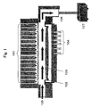
- Fig. 1 is a schematic cross-sectional view of a lamp type light irradiation heat treatment apparatus in the embodiment of the present invention.
- this light irradiation heat treatment apparatus comprises a support element 102 for supporting a workpiece 103 provided in a furnace, plane-shaped light irradiation heating means 101 provided so as to face to one surface of the workpiece 103 supported by the support element 102, temperature measuring means 104 provided so as to face to the other surface at the other side with respect to the one surface of the workpiece 103, light irradiation intensity control means for controlling a light irradiation intensity distribution in a plane of the light irradiation heating means 101 so that a temperature measured by the temperature measuring means 104 may become a predetermined temperature based on a resistivity of the workpiece 103.
- multiple cylindrical lamps (light irradiation heating means) 101 for heating the workpiece, especially a plate-shaped substrate, to raise the temperature thereof are flatly arranged in the apparatus, and the workpiece 103 is supported by the workpiece support element 102 and faces to the multiple lamps 101.
- This support element 102 only supports the workpiece 103 at a very small peripheral portion, and a backside surface of the workpiece 103 is in a state of being exposed.
- a plurality of pyrometers (temperature measuring means) 104 for measuring a temperature are disposed so as to face to the lamp 101 at the opposite side with respect to the workpiece 103.
- the pyrometer 104 measures a wavelength that the workpiece 103 radiates, and determines a temperature of the workpiece 103 based on a value of the measured wavelength.
- inert gas may flow along a surface of the workpiece 103 from an inert gas inlet 105, and be discarded from an inert gas exhaust port 106, and an exhaust gas pump 107 is connected to the end.
- the workpiece 103 is provided with a mechanism for rotating with the support element 102 during a light irradiation heat treatment.
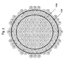
- Fig. 2 shows a plane arrangement view of the lamp in the light irradiation heat treatment apparatus in Fig. 1.
- a plurality of small circles indicate an arrangement of the lamp, and numbers 1 through 12 described in the circles indicate that there exist twelve areas in total which can independently control an electric power (power) supplied to the lamp 101.
- the lamp 101 in the heat treatment apparatus of the embodiment of the present invention is constituted so that the electric power may be independently controlled in the twelve areas.
- a circle 108 indicates a position of the workpiece 103 in a case where a semiconductor substrate having an eight-inch diameter is used as the workpiece 103 disposed so as to face to the lamp 101, and a circle of 109 indicates an outer edge position of the workpiece support element 102.
- a light irradiation heat treatment method of the embodiment of the present invention using the light irradiation heat treatment apparatus which has the above configuration. That is, it includes an open loop control process for raising the temperature of the workpiece 103 at a constant light irradiation intensity up to a controllable temperature of the pyrometer 104, and a closed circuit control process which measures a wavelength that the workpiece 103 radiates by the pyrometer 104, determines the temperature of the workpiece 103 based on the value of the wavelength, and adjusts the light irradiation intensity of the lamp 101.
- an independent power control area of the lamp for heating is split into three areas as shown in Fig. 3.
- the light irradiation intensity of the lamp is split into three areas. They are a circle area 203 existing inside an facing substrate periphery and its radius is equal to a distance 201 from a substrate center (about 80% of the substrate radius having eight-inch diameter), an area 204 existing inside the substrate periphery except the area 203, and an external area 205 of the substrate.
- a radius 202 almost equals to a perimeter of the substrate having eight-inch diameter.
- the workpiece 103 has a circle shape and a flat light intensity distribution from the light irradiation heating means has a concentric circle-shaped distribution.
- a resistivity of the substrate (silicon) is not less than 1 ohm-cm
- the same power is supplied to the lamps both in the area 204 and the area 205 so as to have the same light irradiation intensity, and a light irradiation intensity of the area 203 is made higher than that of the area 204 and the area 205.
- the resistivity of the substrate (silicon) is smaller than 1 ohm-cm
- the same power is supplied to each lamp so that the light irradiation intensity may become constant in all areas of the area 203, the area 204, and the area 205.
- Fig. 5 is a graph showing a change of a temperature with respect to time of the workpiece according to the heat treatment in the prior art. There is shown a change of a temperature of the substrate with respect to time obtained by supplying the same power to all of the multiple lamps 101 in Fig. 1 in a manner similar to the prior art, and making it into a uniform light intensity distribution as shown in Fig. 4B to perform the light irradiation for heating to the substrate.
- a horizontal axis of the graph indicates a light irradiation heat treatment time
- a first axis of vertical axes indicates a temperature of the substrate obtained through measuring a wavelength of the heated substrate radiation by the pyrometer 104 shown in Fig.
- T1 and T6 are symbols which indicate the pyrometers disposed at positions facing to a center and a periphery of the substrate, respectively. These measurement positions of T1 and T6 are shown in Fig. 6.
- T1 corresponds to a temperature at the center of the substrates
- T6 corresponds to a temperature at the peripheral portion. Black dots in the drawing indicate positions of the pyrometers attached to the apparatus, and T1 through T6 indicate symbols of the pyrometers.
- a second axis of the vertical axes is a temperature difference between a portion having the highest temperature and a portion having the lowest temperature within the substrate surface, and it is indicated as delta.
- a used material is a CZ-Si substrate (resistivity: 1-10 ohm-cm), and is typically widely used for manufacturing a semiconductor device.
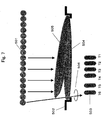
- Reference numeral 501 represents multiple lamps; reference numeral 502, a workpiece support element; reference numeral 503, a plurality of pyrometers; reference numeral 504, a workpiece of a normal position; reference numeral 505, a workpiece which has bounded due to distortion occurrences; and reference numeral 506, a lamp light of the upper part which has leaked from a gap between the substrate and the support element.
- the light 506 enters the pyrometer T6 which is located on the periphery, so that a temperature higher than that of a center is measured.
- the temperature measured here is not a real temperature of the substrate, but the temperature incorrectly measured due to leak of the lamp light, so that in this condition, the measured temperature can not be correctly fed back to an input power control to the lamp. Since this temperature variation is caused by the distortion of the workpiece, it may also be used as an indicator for judging existence of stress.
- Fig. 8 is a graph showing a change of a temperature of the workpiece with respect to time according to the heat treatment of the embodiment of the present invention.
- a substrate temperature change when the heat treatment method of the substrate according to the embodiment of the present invention is used, in other words, at the open loop control process after starting the light irradiation, when a power control is performed to the multiple lamps 101 in the light irradiation heat treatment apparatus in Fig. 1 so as to obtain the light irradiation intensity distribution shown in Fig. 4A.
- a semiconductor substrate used for an experiment in Fig. 8 has a resistivity of 1 to 10 ohm-cm similar to that in Fig. 5.
- the substrate is heated and the temperature thereof is raised based on the light irradiation intensity distribution shown in Fig. 4A at the open loop control process after firstly starting the light irradiation, and after the substrate temperature has been raised not less than a certain temperature or the heating time has passed for a certain time period, the closed circuit control process is performed based on a uniform light irradiation intensity distribution shown in Fig. 4B.
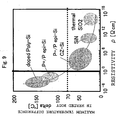
- Fig. 9 is a graph showing a relationship between a resistivity of the workpiece and the maximum temperature difference in the workpiece. It shows a result obtained by applying the open loop control process of the light irradiation rapid heat treatment to substrate materials having various resistivities using the light irradiation intensity distribution shown in Fig. 4A.
- the maximum temperature difference of the graph indicates a difference between the temperatures measured by the pyrometers located in T1 and T6 in Fig. 6.
- the diameter of the substrate is eight inches
- thermal SiO 2 is obtained by forming a thermal oxide film on the a silicon substrate
- SiN is obtained by forming a SiN film on the silicon substrate
- P - /P epi -Si is obtained by growing a P-type epitaxial layer having a medium-concentration on the silicon substrate
- P + /P epi -Si is obtained by forming a P-type epitaxial growth layer having a medium-concentration on the high concentration silicon substrate
- doped Poly-Si is obtained by forming a polysilicon film, into which phosphorus, boron, arsenic or the like is doped, on the silicon substrate.
- the resistivity is not less than 1 ohm-cm
- the maximum temperature difference in the workpiece is not less than 70°C, the undesirable influence will significantly appear in a typical semiconductor device characteristic and reliability, so that the maximum temperature difference not more than 70°C and a resistivity as the whole substrate not less than 1 ohm-cm become a criteria for judgment to perform the open loop control process having the light irradiation intensity distribution.
- the maximum temperature difference may be not less than 70°C by performing the open loop control processs such as shown in Fig.4A; and this is considered that since a response of the substrate to a temperature change and a temperature distribution is fast when the workpiece has a low resistance, the distribution will directly be reflected to the temperature distribution within the substrate when the distribution is given to the light irradiation intensity of the lamp. Therefore, in the embodiment of the present invention, when the resistivity in most of the substrates is not more than 1 ohm-cm, the light irradiation intensity of the lamp of the heat treatment apparatus is made uniform to then perform the open loop control process.
- the light irradiation intensity of the lamp is split into two areas of the area 203 and the area 204 + area 205 as shown in Fig. 4A, but it may be configured such that the light irradiation intensity of the lamp is further split into more areas according to the resistivity of the workpiece, such as semiconductor substrate, and an input electric power and the light irradiation intensity are controlled for every area to form the intensity distribution.
- the apparatus maybe configured such that before performing the light irradiation heat treatment , means (resistivity measurement means) of measuring the resistivity of the workpiece, and means (light irradiation intensity control means) of automatically setting the light intensity to be irradiated for every group area of the lamp so that the distribution may be generated in the light irradiation intensity of the group of the multiple lamps which are flatly provided so as to face to the workpiece based on the measured resistivity of the workpiece are added.
Landscapes
- Furnace Details (AREA)
- Control Of Resistance Heating (AREA)
- Testing Or Measuring Of Semiconductors Or The Like (AREA)
Claims (10)
- Lichtbestrahlungswärmebehandlungsverfahren zum Tragen eines Werkstücks (103) in einem Brennofen und Wärmebehandeln des Werkstücks (103) mittels einer ebenenförmigen Lichtbestrahlungsheizeinrichtung (101), die bereitgestellt ist, um einer Oberfläche des Werkstücks (103) gegenüberzuliegen, wobei das Verfahren umfasst
einen Prozess zum Bestimmen einer Intensitätsverteilung eines von der Lichtbestrahlungsheizeinrichtung (101) eingestrahlten Lichtes auf der Grundlage einer gemessenen Widerstandsgröße des Werkstücks (103), und
einen Prozess zum Einstrahlen eines die bestimmte Lichtintensitätsverteilung aufweisenden Lichtes auf das Werkstück (103) von der Lichtbestrahlungsheizeinrichtung (101), wenn sich die Temperatur des Werkstücks (103) erhöht. - Lichtbestrahlungswärmebehandlungsverfahren gemäß Anspruch 1, wobei das Werkstück (103) ein Siliziumsubstrat enthält, und, wenn eine Widerstandsgröße des Siliziumsubstrats weniger als 1 Ohm-cm beträgt, dann die Intensitätsverteilung des von der Lichtbestrahlungsheizeinrichtung (101) eingestrahlten Lichtes auf eine uniforme Intensitätsverteilung gesetzt wird.
- Lichtbestrahlungswärmebehandlungsverfahren gemäß Anspruch 1, wobei das Werkstück (103) ein Siliziumsubstrat enthält, und, wenn eine Widerstandsgröße des Siliziumsubstrats nicht weniger als 1 Ohm-cm beträgt, dann das von der Lichtbestrahlungsheizeinrichtung (101) eingestrahlte Licht derart gesetzt wird, dass eine Intensitätsverteilung in einem zentralen Bereich (203) kleiner als jene in einem peripheren Bereich (205) sein kann.
- Lichtbestrahlungswärmebehandlungsverfahren gemäß einem der vorstehenden Ansprüche, das ferner einen Prozess zum Einstrahlen eines eine uniforme Intensität aufweisenden Lichtes auf das Werkstück (103) von der Lichtbestrahlungsheizeinrichtung (101) und zum Wärmebehandeln von jenem nach dem Prozess zum Erhöhen der Temperatur des Werkstücks (103) enthält.
- Lichtbestrahlungswärmebehandlungsverfahren gemäß Anspruch 3, wobei die Widerstandsgröße des Siliziumsubstrats nicht weniger als 1 Ohm-cm beträgt, das Siliziumsubstrat eine Kreisform aufweist, und die Lichtintensitätsverteilung von der Wärmebestrahlungsheizeinrichtung (101) eine Verteilung konzentrischer Kreisform ist.
- Lichtbestrahlungswärmebehandlungsvorrichtung, mit
einem Trageelement (102) zum Tragen eines Werkstücks (103), das in einem Brennofen bereitgestellt ist,
einer ebenenförmigen Lichtbestrahlungsheizeinrichtung (101), die bereitgestellt ist, um einer Oberfläche des Werkstücks (103) gegenüberzuliegen, das durch das Trageelement (102) getragen ist,
einer Temperaturmesseinrichtung (104), die bereitgestellt ist, der anderen Oberfläche auf der anderen Seite hinsichtlich der einen Oberfläche des Werkstücks (103) gegenüberzuliegen, und
einer Lichtbestrahlungsintensitätssteuereinrichtung,
dadurch gekennzeichnet, dass die Lichtbestrahlungsintensitätssteuereinrichtung zum Steuern einer Lichtbestrahlungsintensitätsverteilung in einer Ebene der Lichtbestrahlungsheizeinrichtung (101) auf der Grundlage einer gemessenen Widerstandsgröße des Werkstücks (103), wenn sich eine Temperatur des Werkstücks (103) erhöht, eingerichtet ist. - Lichtbestrahlungswärmebehandlungsvorrichtung gemäß Anspruch 6, ferner mit
einer Widerstandsgrößenmesseinrichtung zum Messen der Widerstandsgröße des Werkstücks (103),
wobei die Lichtbestrahlungsintensitätssteuereinrichtung die Lichtbestrahlungsintensitätsverteilung in einer Ebene der Lichtbestrahlungsheizeinrichtung (101) auf der Grundlage der durch die Widerstandsgrößenmesseinrichtung gemessenen Widerstandsgröße des Werkstücks (103) steuert, wenn sich die Temperatur des Werkstücks (103) erhöht. - Lichtbestrahlungswärmebehandlungsvorrichtung gemäß Anspruch 6 oder 7, wobei die Lichtbestrahlungsheizeinrichtung (101) aus einer Gruppe besteht, in der eine Mehrzahl von Wärmelampen flach angeordnet sind, die Gruppe der Wärmelampen in eine Vielzahl von flachen Bereichen (1 bis 12) aufgeteilt ist, und eine voneinander unabhängige Lichtbestrahlungsintensität für jeden Bereich (1 bis 12) gesetzt werden kann.
- Lichtbestrahlungswärmebehandlungsvorrichtung gemäß Anspruch 6 oder 7, wobei die Lichtbestrahlungsintensitätssteuereinrichtung derart steuert, um ein Licht, das eine Lichtbestrahlungsintensitätsverteilung aufweist, die sich in einer Ebene der Lichtbestrahlungsheizeinrichtung (101) ändert, von der Lichtbestrahlungsheizeinrichtung (101) einzustrahlen, wenn das Werkstück (103) ein Siliziumsubstrat ist und die Widerstandsgröße des Werkstücks (103) nicht weniger als 1 Ohm-cm beträgt, und steuert, um ein Licht, das eine uniforme Lichtbestrahlungsintensität in der Ebene der Lichtbestrahlungsheizeinrichtung (101) aufweist, von der Lichtbestrahlungsheizeinrichtung (101) einzustrahlen, wenn die Widerstandsgröße des Siliziumsubstrats weniger als 1 Ohm-cm beträgt.
- Lichtbestrahlungswärmebehandlungsvorrichtung gemäß Anspruch 8, wobei das Werkstück (103) ein Halbleitersubstrat ist und die Gruppe der Wärmelampen in eine Vielzahl von Bereichen (1 bis 12) in einer Form eines flachkonzentrischen Kreise aufgeteilt ist.
Applications Claiming Priority (2)
| Application Number | Priority Date | Filing Date | Title |
|---|---|---|---|
| JP2004011841 | 2004-01-20 | ||
| JP2004011841A JP4024764B2 (ja) | 2004-01-20 | 2004-01-20 | 光照射熱処理方法および光照射熱処理装置 |
Publications (2)
| Publication Number | Publication Date |
|---|---|
| EP1557868A1 EP1557868A1 (de) | 2005-07-27 |
| EP1557868B1 true EP1557868B1 (de) | 2007-07-25 |
Family
ID=34631880
Family Applications (1)
| Application Number | Title | Priority Date | Filing Date |
|---|---|---|---|
| EP04028623A Expired - Lifetime EP1557868B1 (de) | 2004-01-20 | 2004-12-02 | Ein Lichtbestrahlungsverfahren und ein Lichtbestrahlungsapparat |
Country Status (5)
| Country | Link |
|---|---|
| US (1) | US7103271B2 (de) |
| EP (1) | EP1557868B1 (de) |
| JP (1) | JP4024764B2 (de) |
| CN (1) | CN100468654C (de) |
| DE (1) | DE602004007756T2 (de) |
Cited By (1)
| Publication number | Priority date | Publication date | Assignee | Title |
|---|---|---|---|---|
| US8454356B2 (en) | 2006-11-15 | 2013-06-04 | Mattson Technology, Inc. | Systems and methods for supporting a workpiece during heat-treating |
Families Citing this family (14)
| Publication number | Priority date | Publication date | Assignee | Title |
|---|---|---|---|---|
| DE10393962B4 (de) | 2002-12-20 | 2019-03-14 | Mattson Technology Inc. | Verfahren und Vorrichtung zum Stützen eines Werkstücks und zur Wärmebehandlung des Werkstücks |
| US7398693B2 (en) * | 2006-03-30 | 2008-07-15 | Applied Materials, Inc. | Adaptive control method for rapid thermal processing of a substrate |
| JP2008277696A (ja) | 2007-05-07 | 2008-11-13 | Toshiba Corp | 半導体装置の製造方法 |
| JP2008010883A (ja) * | 2007-08-10 | 2008-01-17 | Matsushita Electric Ind Co Ltd | 光照射熱処理方法および光照射熱処理装置 |
| JP5305731B2 (ja) * | 2008-05-12 | 2013-10-02 | キヤノン株式会社 | 半導体素子の閾値電圧の制御方法 |
| KR101610269B1 (ko) * | 2008-05-16 | 2016-04-07 | 맷슨 테크놀로지, 인크. | 워크피스 파손 방지 방법 및 장치 |
| US8254767B2 (en) * | 2008-08-29 | 2012-08-28 | Applied Materials, Inc. | Method and apparatus for extended temperature pyrometry |
| TWI381452B (zh) * | 2008-08-29 | 2013-01-01 | Applied Materials Inc | 用於擴大溫度高溫測定之方法與設備 |
| CN103088415B (zh) * | 2011-11-03 | 2015-12-02 | 上海华虹宏力半导体制造有限公司 | 改善灯加热腔体内温度均匀性的方法 |
| JP6184697B2 (ja) * | 2013-01-24 | 2017-08-23 | 株式会社Screenホールディングス | 熱処理装置および熱処理方法 |
| KR101809141B1 (ko) * | 2014-05-29 | 2018-01-19 | 에이피시스템 주식회사 | 히터 블록 및 기판 열처리 장치 |
| CN106569073B (zh) * | 2016-11-14 | 2020-04-07 | 中国科学院福建物质结构研究所 | 一种基于热电性能测试仪的光致电性能测试附件及方法 |
| CN112725767B (zh) * | 2020-07-06 | 2024-11-15 | 苏州雨竹机电有限公司 | 气相沉积晶圆温度控制结构及方法 |
| CN116453985B (zh) * | 2023-06-19 | 2023-09-08 | 盛吉盛半导体科技(北京)有限公司 | 一种用于半导体设备的快速加热装置 |
Family Cites Families (8)
| Publication number | Priority date | Publication date | Assignee | Title |
|---|---|---|---|---|
| US5053247A (en) | 1989-02-28 | 1991-10-01 | Moore Epitaxial, Inc. | Method for increasing the batch size of a barrel epitaxial reactor and reactor produced thereby |
| JP3824675B2 (ja) | 1995-03-03 | 2006-09-20 | 有限会社デジタル・ウェーブ | 結晶製造装置 |
| US5715361A (en) | 1995-04-13 | 1998-02-03 | Cvc Products, Inc. | Rapid thermal processing high-performance multizone illuminator for wafer backside heating |
| WO1999023690A1 (en) | 1997-11-03 | 1999-05-14 | Asm America, Inc. | Method of processing wafers with low mass support |
| JP3517131B2 (ja) | 1997-11-14 | 2004-04-05 | 株式会社東芝 | 半導体装置の製造方法及び半導体製造装置 |
| JPH11274088A (ja) | 1998-03-23 | 1999-10-08 | Shin Etsu Handotai Co Ltd | 珪素薄膜の製造方法 |
| US6771895B2 (en) * | 1999-01-06 | 2004-08-03 | Mattson Technology, Inc. | Heating device for heating semiconductor wafers in thermal processing chambers |
| TW425635B (en) | 1999-08-23 | 2001-03-11 | Promos Technologies Inc | Rapid thermal processing method and its device |
-
2004
- 2004-01-20 JP JP2004011841A patent/JP4024764B2/ja not_active Expired - Fee Related
- 2004-12-01 US US11/000,223 patent/US7103271B2/en not_active Expired - Lifetime
- 2004-12-02 EP EP04028623A patent/EP1557868B1/de not_active Expired - Lifetime
- 2004-12-02 DE DE602004007756T patent/DE602004007756T2/de not_active Expired - Lifetime
-
2005
- 2005-01-20 CN CNB2005100047691A patent/CN100468654C/zh not_active Expired - Lifetime
Cited By (1)
| Publication number | Priority date | Publication date | Assignee | Title |
|---|---|---|---|---|
| US8454356B2 (en) | 2006-11-15 | 2013-06-04 | Mattson Technology, Inc. | Systems and methods for supporting a workpiece during heat-treating |
Also Published As
| Publication number | Publication date |
|---|---|
| DE602004007756D1 (de) | 2007-09-06 |
| CN1645575A (zh) | 2005-07-27 |
| CN100468654C (zh) | 2009-03-11 |
| JP4024764B2 (ja) | 2007-12-19 |
| US7103271B2 (en) | 2006-09-05 |
| US20050173386A1 (en) | 2005-08-11 |
| DE602004007756T2 (de) | 2008-04-30 |
| EP1557868A1 (de) | 2005-07-27 |
| JP2005209698A (ja) | 2005-08-04 |
Similar Documents
| Publication | Publication Date | Title |
|---|---|---|
| US7103271B2 (en) | Light irradiation heat treatment method and light irradiation heat treatment apparatus | |
| US5297956A (en) | Method and apparatus for heat treating | |
| US4683363A (en) | Microwave apparatus for processing semiconductor | |
| EP3329510B1 (de) | Laserhärten mit rotierendem substrat | |
| US6965092B2 (en) | Ultra fast rapid thermal processing chamber and method of use | |
| US5831249A (en) | Secondary measurement of rapid thermal annealer temperature | |
| JPH0214514A (ja) | 半導体処理の為の急熱炉 | |
| TWI761848B (zh) | 熱處理方法 | |
| JPH10107018A (ja) | 半導体ウェーハの熱処理装置 | |
| US20080037964A1 (en) | Susceptor for heat treatment and heat treatment apparatus | |
| TW201903903A (zh) | 熱處理方法 | |
| US8420555B2 (en) | Manufacturing method for semiconductor device and manufacturing apparatus for semiconductor device | |
| JPH09237789A (ja) | 遮蔽体および熱処理装置および熱処理方法 | |
| JP4143376B2 (ja) | 加熱装置及び半導体素子製造装置用ヒータアセンブリ | |
| CN100334697C (zh) | 半导体器件的制造方法 | |
| JPS61198735A (ja) | フラツシユランプアニ−ル装置 | |
| CN118486609B (zh) | 一种基于新型腔室结构的半导体晶圆退火炉 | |
| JP4079582B2 (ja) | 熱処理装置および熱処理方法 | |
| US7358162B2 (en) | Method of manufacturing semiconductor device | |
| JP2008147656A (ja) | 熱処理装置および熱処理方法 | |
| JPS60137027A (ja) | 光照射加熱方法 | |
| JP2004063895A (ja) | ウェーハ支持リング及び半導体製造装置 | |
| JP2002198320A (ja) | 加熱処理装置、加熱処理方法および半導体装置の製造方法 | |
| JP2004260097A (ja) | 半導体熱処理方法 | |
| CN211265419U (zh) | 一种晶圆热处理设备的边缘环及晶圆热处理设备 |
Legal Events
| Date | Code | Title | Description |
|---|---|---|---|
| PUAI | Public reference made under article 153(3) epc to a published international application that has entered the european phase |
Free format text: ORIGINAL CODE: 0009012 |
|
| AK | Designated contracting states |
Kind code of ref document: A1 Designated state(s): AT BE BG CH CY CZ DE DK EE ES FI FR GB GR HU IE IS IT LI LT LU MC NL PL PT RO SE SI SK TR |
|
| AX | Request for extension of the european patent |
Extension state: AL BA HR LV MK YU |
|
| 17P | Request for examination filed |
Effective date: 20050928 |
|
| AKX | Designation fees paid |
Designated state(s): DE FR GB NL |
|
| 17Q | First examination report despatched |
Effective date: 20051205 |
|
| GRAP | Despatch of communication of intention to grant a patent |
Free format text: ORIGINAL CODE: EPIDOSNIGR1 |
|
| GRAS | Grant fee paid |
Free format text: ORIGINAL CODE: EPIDOSNIGR3 |
|
| GRAA | (expected) grant |
Free format text: ORIGINAL CODE: 0009210 |
|
| AK | Designated contracting states |
Kind code of ref document: B1 Designated state(s): DE FR GB NL |
|
| REG | Reference to a national code |
Ref country code: GB Ref legal event code: FG4D |
|
| REF | Corresponds to: |
Ref document number: 602004007756 Country of ref document: DE Date of ref document: 20070906 Kind code of ref document: P |
|
| ET | Fr: translation filed | ||
| PLBE | No opposition filed within time limit |
Free format text: ORIGINAL CODE: 0009261 |
|
| STAA | Information on the status of an ep patent application or granted ep patent |
Free format text: STATUS: NO OPPOSITION FILED WITHIN TIME LIMIT |
|
| 26N | No opposition filed |
Effective date: 20080428 |
|
| PGFP | Annual fee paid to national office [announced via postgrant information from national office to epo] |
Ref country code: NL Payment date: 20091216 Year of fee payment: 6 |
|
| REG | Reference to a national code |
Ref country code: NL Ref legal event code: V1 Effective date: 20110701 |
|
| PG25 | Lapsed in a contracting state [announced via postgrant information from national office to epo] |
Ref country code: NL Free format text: LAPSE BECAUSE OF NON-PAYMENT OF DUE FEES Effective date: 20110701 |
|
| PGFP | Annual fee paid to national office [announced via postgrant information from national office to epo] |
Ref country code: DE Payment date: 20121128 Year of fee payment: 9 |
|
| PGFP | Annual fee paid to national office [announced via postgrant information from national office to epo] |
Ref country code: GB Payment date: 20121128 Year of fee payment: 9 |
|
| PGFP | Annual fee paid to national office [announced via postgrant information from national office to epo] |
Ref country code: FR Payment date: 20130107 Year of fee payment: 9 |
|
| REG | Reference to a national code |
Ref country code: DE Ref legal event code: R119 Ref document number: 602004007756 Country of ref document: DE |
|
| GBPC | Gb: european patent ceased through non-payment of renewal fee |
Effective date: 20131202 |
|
| REG | Reference to a national code |
Ref country code: DE Ref legal event code: R119 Ref document number: 602004007756 Country of ref document: DE Effective date: 20140701 |
|
| REG | Reference to a national code |
Ref country code: FR Ref legal event code: ST Effective date: 20140829 |
|
| PG25 | Lapsed in a contracting state [announced via postgrant information from national office to epo] |
Ref country code: DE Free format text: LAPSE BECAUSE OF NON-PAYMENT OF DUE FEES Effective date: 20140701 |
|
| PG25 | Lapsed in a contracting state [announced via postgrant information from national office to epo] |
Ref country code: FR Free format text: LAPSE BECAUSE OF NON-PAYMENT OF DUE FEES Effective date: 20131231 Ref country code: GB Free format text: LAPSE BECAUSE OF NON-PAYMENT OF DUE FEES Effective date: 20131202 |