EP1555853A2 - Masque, procédé de préparation, procédé de preparation d'un dispositif électroluminescent et dispositif électroluminescent - Google Patents
Masque, procédé de préparation, procédé de preparation d'un dispositif électroluminescent et dispositif électroluminescent Download PDFInfo
- Publication number
- EP1555853A2 EP1555853A2 EP04028352A EP04028352A EP1555853A2 EP 1555853 A2 EP1555853 A2 EP 1555853A2 EP 04028352 A EP04028352 A EP 04028352A EP 04028352 A EP04028352 A EP 04028352A EP 1555853 A2 EP1555853 A2 EP 1555853A2
- Authority
- EP
- European Patent Office
- Prior art keywords
- substrate
- mask
- manufacturing
- bonded
- mask according
- Prior art date
- Legal status (The legal status is an assumption and is not a legal conclusion. Google has not performed a legal analysis and makes no representation as to the accuracy of the status listed.)
- Withdrawn
Links
- 238000000034 method Methods 0.000 title claims description 35
- 238000004519 manufacturing process Methods 0.000 title claims description 25
- 239000000758 substrate Substances 0.000 claims abstract description 214
- 239000000853 adhesive Substances 0.000 claims description 32
- 239000000463 material Substances 0.000 claims description 21
- 238000010030 laminating Methods 0.000 claims description 12
- XUIMIQQOPSSXEZ-UHFFFAOYSA-N Silicon Chemical compound [Si] XUIMIQQOPSSXEZ-UHFFFAOYSA-N 0.000 claims description 6
- 229910052710 silicon Inorganic materials 0.000 claims description 6
- 239000010703 silicon Substances 0.000 claims description 6
- 238000000151 deposition Methods 0.000 description 15
- 230000008021 deposition Effects 0.000 description 14
- 239000011521 glass Substances 0.000 description 12
- 238000005452 bending Methods 0.000 description 7
- 238000005530 etching Methods 0.000 description 6
- 239000000696 magnetic material Substances 0.000 description 5
- 229910052751 metal Inorganic materials 0.000 description 4
- 239000002184 metal Substances 0.000 description 4
- 239000007769 metal material Substances 0.000 description 4
- 239000011368 organic material Substances 0.000 description 4
- PXHVJJICTQNCMI-UHFFFAOYSA-N Nickel Chemical compound [Ni] PXHVJJICTQNCMI-UHFFFAOYSA-N 0.000 description 3
- 238000010586 diagram Methods 0.000 description 3
- 230000001070 adhesive effect Effects 0.000 description 2
- 230000015572 biosynthetic process Effects 0.000 description 2
- 229910021419 crystalline silicon Inorganic materials 0.000 description 2
- 238000005520 cutting process Methods 0.000 description 2
- 230000005525 hole transport Effects 0.000 description 2
- 238000012986 modification Methods 0.000 description 2
- 230000004048 modification Effects 0.000 description 2
- 229910052759 nickel Inorganic materials 0.000 description 2
- 238000000059 patterning Methods 0.000 description 2
- 229920000553 poly(phenylenevinylene) Polymers 0.000 description 2
- 239000011347 resin Substances 0.000 description 2
- 229920005989 resin Polymers 0.000 description 2
- 238000004544 sputter deposition Methods 0.000 description 2
- 239000004593 Epoxy Substances 0.000 description 1
- 238000003848 UV Light-Curing Methods 0.000 description 1
- 229910052782 aluminium Inorganic materials 0.000 description 1
- XAGFODPZIPBFFR-UHFFFAOYSA-N aluminium Chemical compound [Al] XAGFODPZIPBFFR-UHFFFAOYSA-N 0.000 description 1
- 229910017052 cobalt Inorganic materials 0.000 description 1
- 239000010941 cobalt Substances 0.000 description 1
- GUTLYIVDDKVIGB-UHFFFAOYSA-N cobalt atom Chemical compound [Co] GUTLYIVDDKVIGB-UHFFFAOYSA-N 0.000 description 1
- 238000001723 curing Methods 0.000 description 1
- 238000011161 development Methods 0.000 description 1
- 230000018109 developmental process Effects 0.000 description 1
- 238000013007 heat curing Methods 0.000 description 1
- 150000002500 ions Chemical class 0.000 description 1
- -1 poly(para-phenylene vinylene) Polymers 0.000 description 1
- 229910001256 stainless steel alloy Inorganic materials 0.000 description 1
- TVIVIEFSHFOWTE-UHFFFAOYSA-K tri(quinolin-8-yloxy)alumane Chemical compound [Al+3].C1=CN=C2C([O-])=CC=CC2=C1.C1=CN=C2C([O-])=CC=CC2=C1.C1=CN=C2C([O-])=CC=CC2=C1 TVIVIEFSHFOWTE-UHFFFAOYSA-K 0.000 description 1
Images



Classifications
-
- H—ELECTRICITY
- H05—ELECTRIC TECHNIQUES NOT OTHERWISE PROVIDED FOR
- H05B—ELECTRIC HEATING; ELECTRIC LIGHT SOURCES NOT OTHERWISE PROVIDED FOR; CIRCUIT ARRANGEMENTS FOR ELECTRIC LIGHT SOURCES, IN GENERAL
- H05B33/00—Electroluminescent light sources
- H05B33/10—Apparatus or processes specially adapted to the manufacture of electroluminescent light sources
-
- H—ELECTRICITY
- H10—SEMICONDUCTOR DEVICES; ELECTRIC SOLID-STATE DEVICES NOT OTHERWISE PROVIDED FOR
- H10K—ORGANIC ELECTRIC SOLID-STATE DEVICES
- H10K71/00—Manufacture or treatment specially adapted for the organic devices covered by this subclass
- H10K71/10—Deposition of organic active material
- H10K71/16—Deposition of organic active material using physical vapour deposition [PVD], e.g. vacuum deposition or sputtering
- H10K71/166—Deposition of organic active material using physical vapour deposition [PVD], e.g. vacuum deposition or sputtering using selective deposition, e.g. using a mask
Definitions
- the present invention relates to a mask and a method for manufacturing thereof, to a method for manufacturing an organic electroluminescent (EL) device, and to an organic EL device.
- EL organic electroluminescent
- a deposition pattern is selectively formed through a mask so as to separately colour each red, blue, and green luminescent layer on a glass substrate.
- a metal mask is used as the mask
- deposition is conducted in a condition where the mask is adhered to one side of the glass substrate by a permanent magnet placed on the other side of the glass substrate.
- a permanent magnet placed on the other side of the glass substrate.
- a position of the mask deviates from that of the glass substrate, since there is a large difference between a thermal expansion coefficient of the mask and that of the glass substrate.
- Japanese Unexamined Patent Publication No. 2003-100460 discloses a technique in which the mask strength is increased by mounting a plurality of small Si mask chips on a large-sized substrate material provided with apertures.
- the present invention aims at providing a mask that is reliable, for example, for deposition and that can form a desired high-precision layer pattern on, for example, a glass substrate used as a layer-formation object material, and a method for manufacturing thereof. Further, the present invention aims to provide a method for manufacturing an organic EL device using the mask.
- the mask of the present invention includes a first substrate having a first aperture and at least one second substrate having second apertures serving as mask apertures of the mask of the invention, wherein the second apertures are placed in the first aperture and the at least one second substrate is partially bonded to the first substrate.
- the mask shall have a very high strength.
- the second substrate and the first substrate can be bonded with an adhesive agent, which can be formed partially on one second substrate.
- an adhesive agent which can be formed partially on one second substrate.
- a desired high-precision layer pattern can be formed.
- the bonding procedure using an adhesive agent is very simple, it is possible to provide the mask at a low cost.
- the second substrate can have a structure in that it can be bonded to the first substrate over a plurality of points, and that, when an adhesive agent is used as described, the adhesive agent can be arranged over a plurality of places for one second substrate.
- the second substrate is formed rectangularly, and only a corner of the second substrate is partially bonded to the first substrate. Also, it is possible that only one side of each second substrate that opposes the other side of a primary surface of the respective second substrate is bonded partially to the first substrate. Moreover, the second substrate can be bonded partially to the first substrate close to a center of a side having the largest expansion of all sides of a primary surface of the second substrate. In any of these structures, a desired high-precision layer pattern can be formed.using the mask.
- more than two second substrates can be bonded to the first substrate sharing the same adhesive agent. This can simplify the adhesive agent supply procedure at the same time as it can form a desired high-precision layer pattern using the mask.
- an alignment mark used when bonding the second substrate to the first substrate can be placed on each substrate, with each substrate being bonded in close proximity to the alignment mark.
- the procedure for aligning the first substrate and the second substrate will be relatively easy compared to when forming the bonding portion apart from an alignment mark.
- the second substrate can be formed with a silicon wafer.
- the difference between a thermal expansion coefficient of the mask and that of the glass substrate or the like as a layer-formation object material will be smaller, preventing the position of the mask from deviating from the position of the layer-formation object material.
- the method for manufacturing the mask of the present invention includes the steps of: laminating a first substrate having a first aperture and at least one second substrate having second apertures serving as mask apertures so that the second apertures are placed in the first aperture, and, in the laminating step, partially bonding the at least one second substrate to the first substrate.
- the above-described mask of the present invention can be suitably manufactured.
- the second substrate is partially bonded to the first substrate preferably using an adhesive agent, which is partially formed on the first substrate and/or the second substrate.
- the second substrate may be partially bonded to the first substrate in the laminating step. Also, in the laminating step, only one side each that opposes the other of the second substrate may be partially bonded to the first substrate. Moreover, in the laminating step, the second substrate may be partially bonded to the first substrate close to a center of a side having the largest expansion coefficient of all sides of a primary surface of the second substrate.
- the method of manufacturing an organic EL device according to the present invention includes forming an organic EL element using the mask of the present invention.
- a luminescent material organic material
- a luminescent layer for example, can be formed into a layer by deposition.
- a highly reliable organic EL device having a luminescent layer in a predetermined pattern may be obtained.
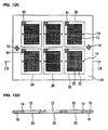
- FIG. 1(A) is a flat pattern view of the mask according to an embodiment of the present invention
- FIG. 1(B) is a cross sectional view taken on a IB-IB line of FIG. 1(A).
- FIG. 2(A) is a flat pattern view of an enlarged principal part of the mask in accordance with the embodiment of the present invention
- FIG. 2(B) is a cross sectional view taken on a IIB-IIB line of FIG. 2(A).
- the mask of the present embodiment is composed of a first substrate 10 and at least one (in FIG. 1(A), a plurality of) second substrate 20.
- FIG. 3 is a flat pattern view showing a rough structure of the first substrate 10
- FIG. 4 is a flat pattern view showing a rough structure of the second substrate 20.
- the first substrate 10 may be composed of a transparent substrate such as a glass substrate.
- a transparent substrate such as a glass substrate.
- a plurality of aperture is formed rectangularly so that the second substrates 20 can be fit into the apertures 12. Therefore the first substrate 10 may be called frames.
- an area of the aperture 12 is structured to be smaller than an area of a primary surface of the second substrate 20.
- the aperture 12 is larger than a region on the second substrate 20 on which a plurality of through-holes 22 are formed, as will be described later.
- a first alignment mark 14 is formed on the first substrate 10.
- the first alignment mark 14 is used for aligning the first substrate 10 with the second substrate 20 when bonding them together.
- the first alignment mark 14 may be formed with a metal film or by etching.
- a mask-positioning mark 16 is formed on the first substrate 10.
- the mask-positioning mark 16 is used for positioning the mask of the present embodiment when conducting deposition using the mask.
- the mask-positioning mark 16 can also be formed with a metal material. Further, the mask-positioning mark 16 may be formed on the second substrate 20.
- the second substrate 20 is formed rectangularly, similarly outlining the aperture 12, and a plurality of through-holes 22 (see FIG. 2(A) and FIG. 2(B)) are formed thereon.
- the through-hole 22 may be in any shape as square, parallelogram, or circular.
- a mask pattern is structured relative to the shape, arrangement, and quantity of the through-holes 22. Therefore, the second substrate 20 may be called a screen board.
- a second alignment mark 24 is formed on the second substrate 20 .
- the first and the second substrates 10 and 20 are aligned with each other using the first and the second alignment marks 14 and 24.
- the second alignment mark 24 may be formed by etching the second substrate 20 or may be formed with a metal film.
- a plurality of second substrates 20 are mounted on the first substrate 10. As shown in FIG. 2(A), the second substrate 20 is mounted on the first substrate 10, in that a plurality of through-holes 22 are arranged inside the aperture 12 on the first substrate 10. More precisely, a periphery of the second substrate 20 is mounted along a rim of the aperture 12 of the first substrate 10, and one second substrate 20 is mounted corresponding to one aperture 12. The second substrate 20 is mounted on a surface of the first substrate 10 opposite the surface of the other side where the first alignment mark 14 is formed. In the present embodiment, the first and the second substrates 10 and 20 are laminated with an adhesive agent 91, and the second substrate 20 is composed of a material adhesive to the first substrate 10 (such as silicon).
- the adhesive agent 91 is formed partially on a corner of the second substrate 20, which is bonded to the first substrate 10 only at the corner. Therefore, when an adhesive agent is applied along the entire periphery of the second substrate 20, a degree of freedom of the substrates increases in comparison with a structure in which the entire periphery is adhered to the first substrate 10. Even if there is a case in which the second substrate 20 is expanded due to heat or the like in the adhering procedure, a problem of the bending on the second substrate 20 does not easily take place.
- FIG. 5 shows a cross sectional pattern view for describing the method for manufacturing the mask in accordance with the present embodiment.
- the first substrate 10 composed of glass and the second substrate 20 composed of single crystalline silicon.
- sandblast may be applied.
- the first alignment mark 14 or the mask-positioning mark 16 on the first substrate 10 may be formed by, for example, sputtering or deposition, or by etching.
- a plurality of through-holes 22 are formed on the second substrate 20, a plurality of through-holes 22 are formed.
- etching e.g. anisotropic etching having crystal-surface orientation dependency
- a wall surface of the through-hole 22 may be perpendicular to the surface (primary surface) of the second substrate 20 or may be tapered.
- the second substrate 20 when forming the second substrate 20 using a silicon wafer 26, the second substrate 20 can be obtained by cutting the silicon wafer 26 into a desired shape. By this method, a flatness (greatest height) - (smallest height) of the second substrate 20 is around 5 ⁇ m.
- the second alignment mark 24 on the second substrate 20 may be formed by etching, or by sputtering or deposition, for example.
- the adhesive agent 91 is applied to one corner of the periphery of each aperture 12 of the first substrate 10.
- a highly adhesive, epoxy UV curing adhesive agent (light curing resin) with low outgas in vacuum may be employed, or a heat curing resin may be employed.
- the adhesive agent 91 may be applied, for example, to one corner of the rectangular second substrate 20 or to both corners of the first substrate 10 and the second substrate 20.
- first substrate 10 and the second substrate 20 are then aligned with each other, bonded with the adhesive agent 91 which has been applied thereon.
- a plurality of second substrates 20 are arranged on one surface of the first substrate 10 in such a way that the second substrates 20 do not overlap one another.
- the first and the second alignment marks 14 and 24 are used for their alignment. After aligning, the first and the second substrates 10 and 20 are adhered to each other by illuminating the adhesive agent 91.
- the second substrate 20 is reinforced by the first substrate 10, enabling a mask to be manufactured with a high strength. Further, even when expansion or shrinkage occurs on the first and/or the second substrate 10 and/or 20, the expansion or shrinkage on the substrates will be lessened at the non-bonded (non-adhered) part since the adhesive agent 91 is applied to only one corner for bonding, and, therefore, a problem such as the bending on the substrates will be solved. As a result, a gap between a layer-formation object material and the mask will not easily appear, and thereby the mask of the present embodiment having a desired high-precision layer pattern can be formed by, for example, deposition.
- the surfaces of the second substrates 20 may be polished by a whetstone 40 or the like. This enables the flattening of a plurality of the surfaces of the second substrates 20, thereby increasing adhesion to objects to which deposition, for example, is conducted.
- FIG. 7 is a diagram showing alternative examples of the present embodiment. That is, it illustrates various places at which the adhesive agent 91 may be applied.
- An adhesive agent 91a may be applied not only on a corner of the aperture 12 as shown in FIG. 1(A), but also on one side of the aperture 12 as shown in FIG. 7(a). Further, as shown in FIG. 7(b), an adhesive agent 91b may be applied close to the center of one side of the aperture 12.
- an adhesive agent 91c may be applied on more than one side of the aperture 12, particularly only on one side each that opposes the other side.
- an adhesive agent 91c is to be applied on two sides constituting a corner.
- the adhesive agent 91d may be applied close to the center of each side of the aperture 12 as shown in FIG. 7(d).
- an adhesive agent close to the center of the side having the largest expansion coefficient of all sides of the aperture 12 a degree of freedom of substrates increases further, which can prevent or restrain the bending on the substrates caused by, for example, heat expansion.
- an adhesive agent 91e may be applied sharing among a plurality of apertures 12.
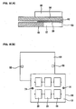
- FIG. 8(A) and FIG. 8(B) illustrate the method for manufacturing the organic EL in accordance with the embodiment of the present invention.
- a magnetic material layer 52 is formed on a mask 50 (e.g. the second substrate 20) shown in FIG. 8(A).
- the magnetic material layer 52 may be formed with a strongly magnetic material such as ion, cobalt, or nickel.
- a magnetic metal material such as Ni, Co, Fe, or a stainless steel alloy containing Fe, or a combination of a magnetic metal material and a nonmagnetic metal material may be used to form the magnetic material layer 52.
- Other details on the mask 50 are as described above.
- a luminescent material is formed into a layer on a substrate (layer-formation object material) 54 using the mask 50.
- the substrate 54 is used for forming a plurality of organic EL devices and is a transparent substrate such as a glass substrate.
- an electrode e.g. a transparent electrode composed of an ITO, for example
- a hole transport layer 58 is formed, or, alternatively, an electron transport layer may be formed.
- the mask 50 is arranged so that the second substrate 20 is placed on one side of the substrate 54.
- a magnet 48 is placed so as to attract the magnetic material layer 52 formed on the mask 50 (the second substrate 20).
- FIG. 8(B) is a diagram for describing the method for positioning the mask.
- the mask-positioning mark 16 is formed on the first substrate 10.
- a positioning mark 55 is formed on the substrate 54. Using the mask-positioning mark 16 and the positioning mark 55, the first substrate 10 and the substrate 54 are aligned with each other.
- the luminescent material is an organic material, for example.
- a low-molecular organic material there is tri(8-hydrooxyquinoline) aluminum (Alq 3 ), and as a high-molecular organic material, there is poly(para-phenylene vinylene) (PPV).
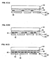
- the luminescent material may be formed into a layer by deposition. For example, as shown in FIG. 9(A), a red luminescent material is patterned through the mask to form a red luminescent layer 60. Then, as shown in FIG.
- a green luminescent layer 62 is formed. Also, as shown in FIG. 9(C), by moving the mask 50 again and by patterning a blue luminescent material, a blue luminescent layer 64 is formed.
- the second substrate 20 serving as a screen is partially bonded to the first substrate 10. Therefore, the second substrate 20 has a high degree of freedom and does not easily bend or deform and shows a high repeatability in the selective deposition and high productivity.
- the mask 50 of the present embodiment a plurality of the apertures 12 are formed on the first substrate 10, and the second substrates 20 are placed corresponding to each aperture 12.
- Each second substrate 20 corresponds to one organic EL device. In other words, by using the mask 50, a plurality of unified organic EL devices can be manufactured. By cutting the substrate 54, separate organic EL devices can be obtained.
- FIG. 10 is a flat pattern view illustrating a rough structure of the organic EL device manufactured by following the above-described method for forming the layers of the luminescent materials.
- the organic EL device includes the substrate 54, the electrode 56, the hole transport layer 58, and the luminescent layers 60, 62, and 64. On the luminescent layers 60, 62, and 64, an electrode 66 is formed.
- the electrode 66 is a cathode electrode, for example.
- the organic EL device such as this is suitable for a display device (or a display), and by using the luminescent layers 60, 62, and 64, a highly reliable display with a very little pattern shifting can be provided.
- a mobile phone 500 is illustrated in FIG. 11.
- the mobile phone has a structure having a display unit 501 which includes the organic EL device of the above-described embodiment, thereby a very highly reliable display can be provided.
Landscapes
- Engineering & Computer Science (AREA)
- Manufacturing & Machinery (AREA)
- Electroluminescent Light Sources (AREA)
- Physical Vapour Deposition (AREA)
Applications Claiming Priority (2)
| Application Number | Priority Date | Filing Date | Title |
|---|---|---|---|
| JP2003403070A JP2005163099A (ja) | 2003-12-02 | 2003-12-02 | マスク、マスクの製造方法、有機el装置の製造方法、有機el装置 |
| JP2003403070 | 2003-12-02 |
Publications (1)
| Publication Number | Publication Date |
|---|---|
| EP1555853A2 true EP1555853A2 (fr) | 2005-07-20 |
Family
ID=34616768
Family Applications (1)
| Application Number | Title | Priority Date | Filing Date |
|---|---|---|---|
| EP04028352A Withdrawn EP1555853A2 (fr) | 2003-12-02 | 2004-11-30 | Masque, procédé de préparation, procédé de preparation d'un dispositif électroluminescent et dispositif électroluminescent |
Country Status (6)
| Country | Link |
|---|---|
| US (1) | US20050118788A1 (fr) |
| EP (1) | EP1555853A2 (fr) |
| JP (1) | JP2005163099A (fr) |
| KR (1) | KR100683336B1 (fr) |
| CN (1) | CN1625311A (fr) |
| TW (1) | TW200520609A (fr) |
Cited By (1)
| Publication number | Priority date | Publication date | Assignee | Title |
|---|---|---|---|---|
| TWI383245B (zh) * | 2007-01-24 | 2013-01-21 | Sharp Kk | 用於成形微透鏡之使用多段式光微影製造灰階遮罩的方法 |
Families Citing this family (27)
| Publication number | Priority date | Publication date | Assignee | Title |
|---|---|---|---|---|
| US20060141744A1 (en) * | 2004-12-27 | 2006-06-29 | Asml Netherlands B.V. | System and method of forming a bonded substrate and a bonded substrate product |
| JP4285456B2 (ja) * | 2005-07-20 | 2009-06-24 | セイコーエプソン株式会社 | マスク、マスクの製造方法、成膜方法及び電気光学装置の製造方法 |
| JP5328726B2 (ja) | 2009-08-25 | 2013-10-30 | 三星ディスプレイ株式會社 | 薄膜蒸着装置及びこれを利用した有機発光ディスプレイ装置の製造方法 |
| JP5677785B2 (ja) | 2009-08-27 | 2015-02-25 | 三星ディスプレイ株式會社Samsung Display Co.,Ltd. | 薄膜蒸着装置及びこれを利用した有機発光表示装置の製造方法 |
| US20110052795A1 (en) * | 2009-09-01 | 2011-03-03 | Samsung Mobile Display Co., Ltd. | Thin film deposition apparatus and method of manufacturing organic light-emitting display device by using the same |
| US8876975B2 (en) | 2009-10-19 | 2014-11-04 | Samsung Display Co., Ltd. | Thin film deposition apparatus |
| KR101084184B1 (ko) | 2010-01-11 | 2011-11-17 | 삼성모바일디스플레이주식회사 | 박막 증착 장치 |
| KR101193186B1 (ko) | 2010-02-01 | 2012-10-19 | 삼성디스플레이 주식회사 | 박막 증착 장치, 이를 이용한 유기 발광 디스플레이 장치의 제조방법 및 이에 따라 제조된 유기 발광 디스플레이 장치 |
| KR101232181B1 (ko) * | 2010-02-03 | 2013-02-12 | 엘지디스플레이 주식회사 | 마스크 어셈블리 |
| KR101156441B1 (ko) | 2010-03-11 | 2012-06-18 | 삼성모바일디스플레이주식회사 | 박막 증착 장치 |
| US8894458B2 (en) | 2010-04-28 | 2014-11-25 | Samsung Display Co., Ltd. | Thin film deposition apparatus, method of manufacturing organic light-emitting display device by using the apparatus, and organic light-emitting display device manufactured by using the method |
| KR101223723B1 (ko) | 2010-07-07 | 2013-01-18 | 삼성디스플레이 주식회사 | 박막 증착 장치, 이를 이용한 유기 발광 디스플레이 장치의 제조방법 및 이에 따라 제조된 유기 발광 디스플레이 장치 |
| KR101723506B1 (ko) | 2010-10-22 | 2017-04-19 | 삼성디스플레이 주식회사 | 유기층 증착 장치 및 이를 이용한 유기 발광 디스플레이 장치의 제조 방법 |
| KR20120045865A (ko) | 2010-11-01 | 2012-05-09 | 삼성모바일디스플레이주식회사 | 유기층 증착 장치 |
| KR20120057290A (ko) | 2010-11-26 | 2012-06-05 | 삼성모바일디스플레이주식회사 | 박막 증착 장치 |
| KR101759347B1 (ko) * | 2010-12-14 | 2017-08-01 | 삼성디스플레이 주식회사 | 박막 증착용 마스크 프레임 조립체 및 그 제조방법 |
| KR101760897B1 (ko) | 2011-01-12 | 2017-07-25 | 삼성디스플레이 주식회사 | 증착원 및 이를 구비하는 유기막 증착 장치 |
| KR101852517B1 (ko) | 2011-05-25 | 2018-04-27 | 삼성디스플레이 주식회사 | 유기층 증착 장치 및 이를 이용한 유기 발광 디스플레이 장치의 제조 방법 |
| KR101857249B1 (ko) | 2011-05-27 | 2018-05-14 | 삼성디스플레이 주식회사 | 패터닝 슬릿 시트 어셈블리, 유기막 증착 장치, 유기 발광 표시장치제조 방법 및 유기 발광 표시 장치 |
| KR101826068B1 (ko) | 2011-07-04 | 2018-02-07 | 삼성디스플레이 주식회사 | 유기층 증착 장치 |
| CN102492920A (zh) * | 2011-12-21 | 2012-06-13 | 信利半导体有限公司 | 一种制作掩膜板的方法和掩膜板 |
| CN107858642B (zh) * | 2013-04-12 | 2020-04-21 | 大日本印刷株式会社 | 蒸镀掩模、蒸镀掩模准备体、蒸镀掩模的制造方法、及有机半导体元件的制造方法 |
| JP6142393B2 (ja) * | 2013-09-09 | 2017-06-07 | 株式会社ブイ・テクノロジー | 成膜マスク、成膜装置及び成膜方法並びにタッチパネル基板 |
| JP6326885B2 (ja) * | 2014-03-19 | 2018-05-23 | 大日本印刷株式会社 | 蒸着マスク、蒸着マスク準備体、及び有機半導体素子の製造方法 |
| US10995140B2 (en) * | 2015-06-05 | 2021-05-04 | H. Lee Moffitt Cancer Center And Research Institute, Inc. | GM-CSF/CD40L vaccine and checkpoint inhibitor combination therapy |
| CN111223399A (zh) * | 2018-11-27 | 2020-06-02 | 中华映管股份有限公司 | 柔性显示面板的制作方法 |
| JP7291514B2 (ja) * | 2019-03-27 | 2023-06-15 | 日東電工株式会社 | 配線回路基板およびその製造方法 |
Family Cites Families (5)
| Publication number | Priority date | Publication date | Assignee | Title |
|---|---|---|---|---|
| JP3695177B2 (ja) * | 1998-10-29 | 2005-09-14 | 日立電線株式会社 | 半導体装置用中間製品 |
| JP2001237073A (ja) * | 2000-02-24 | 2001-08-31 | Tohoku Pioneer Corp | 多面取り用メタルマスク及びその製造方法 |
| JP3651432B2 (ja) * | 2001-09-25 | 2005-05-25 | セイコーエプソン株式会社 | マスク及びその製造方法並びにエレクトロルミネッセンス装置の製造方法 |
| JP2003231964A (ja) * | 2001-12-05 | 2003-08-19 | Toray Ind Inc | 蒸着マスクおよびその製造方法並びに有機電界発光装置およびその製造方法 |
| JP2004183044A (ja) * | 2002-12-03 | 2004-07-02 | Seiko Epson Corp | マスク蒸着方法及び装置、マスク及びマスクの製造方法、表示パネル製造装置、表示パネル並びに電子機器 |
-
2003
- 2003-12-02 JP JP2003403070A patent/JP2005163099A/ja not_active Withdrawn
-
2004
- 2004-11-23 CN CNA2004100950941A patent/CN1625311A/zh active Pending
- 2004-11-30 TW TW093136907A patent/TW200520609A/zh unknown
- 2004-11-30 EP EP04028352A patent/EP1555853A2/fr not_active Withdrawn
- 2004-12-01 US US11/001,497 patent/US20050118788A1/en not_active Abandoned
- 2004-12-01 KR KR1020040099826A patent/KR100683336B1/ko not_active Expired - Fee Related
Cited By (1)
| Publication number | Priority date | Publication date | Assignee | Title |
|---|---|---|---|---|
| TWI383245B (zh) * | 2007-01-24 | 2013-01-21 | Sharp Kk | 用於成形微透鏡之使用多段式光微影製造灰階遮罩的方法 |
Also Published As
| Publication number | Publication date |
|---|---|
| TW200520609A (en) | 2005-06-16 |
| JP2005163099A (ja) | 2005-06-23 |
| KR20050053334A (ko) | 2005-06-08 |
| CN1625311A (zh) | 2005-06-08 |
| KR100683336B1 (ko) | 2007-02-15 |
| US20050118788A1 (en) | 2005-06-02 |
Similar Documents
| Publication | Publication Date | Title |
|---|---|---|
| EP1555853A2 (fr) | Masque, procédé de préparation, procédé de preparation d'un dispositif électroluminescent et dispositif électroluminescent | |
| KR100484023B1 (ko) | 마스크 및 그 제조 방법, 및 일렉트로루미네선스 장치의 제조 방법 | |
| KR100641478B1 (ko) | 마스크 증착 방법 및 장치, 마스크 및 마스크의 제조 방법 및 표시 패널 제조 장치 | |
| CN100482851C (zh) | 掩模成膜方法,掩模 | |
| KR101122585B1 (ko) | 유기발광 표시장치의 제조방법 | |
| JP4418262B2 (ja) | 基板・マスク固定装置 | |
| CN101675178A (zh) | 基板处理设备及基板处理方法 | |
| KR100727722B1 (ko) | 마스크 지지 구조, 성막 방법, 전기 광학 장치의 제조 방법및 전자기기 | |
| KR100755352B1 (ko) | 마스크, 마스크의 제조 방법, 패턴 형성 장치, 패턴 형성방법 | |
| JP2003173872A (ja) | アライメント方法、パターン形成方法及びアライメント装置、並びに有機エレクトロルミネッセンス表示装置及びその製造方法 | |
| KR100484024B1 (ko) | 마스크 및 그 제조 방법, 일렉트로루미네선스 장치 및 그제조 방법, 및 전자 기기 | |
| CN100459222C (zh) | 掩模及其制法、薄膜图案的形成方法、电光学装置的制法 | |
| JP2003272838A (ja) | マスキング部材 | |
| CN109837519B (zh) | 成膜装置、成膜方法及有机el显示装置的制造方法 | |
| KR102794838B1 (ko) | 새도우 마스크 제조 방법 및 새도우 마스크 | |
| KR100671975B1 (ko) | 대면적의 유기전계발광소자 제조용 섀도우 마스크 및 그제조방법 | |
| JP2004335486A (ja) | マスク及びその製造方法、エレクトロルミネッセンス装置及びその製造方法並びに電子機器 |
Legal Events
| Date | Code | Title | Description |
|---|---|---|---|
| PUAI | Public reference made under article 153(3) epc to a published international application that has entered the european phase |
Free format text: ORIGINAL CODE: 0009012 |
|
| AK | Designated contracting states |
Kind code of ref document: A2 Designated state(s): AT BE BG CH CY CZ DE DK EE ES FI FR GB GR HU IE IS IT LI LU MC NL PL PT RO SE SI SK TR |
|
| AX | Request for extension of the european patent |
Extension state: AL HR LT LV MK YU |
|
| STAA | Information on the status of an ep patent application or granted ep patent |
Free format text: STATUS: THE APPLICATION HAS BEEN WITHDRAWN |
|
| 18W | Application withdrawn |
Effective date: 20090122 |