EP1554569B1 - Sensor-anordnung und verfahren zum betreiben einer sensor-anordnung - Google Patents
Sensor-anordnung und verfahren zum betreiben einer sensor-anordnung Download PDFInfo
- Publication number
- EP1554569B1 EP1554569B1 EP03772214A EP03772214A EP1554569B1 EP 1554569 B1 EP1554569 B1 EP 1554569B1 EP 03772214 A EP03772214 A EP 03772214A EP 03772214 A EP03772214 A EP 03772214A EP 1554569 B1 EP1554569 B1 EP 1554569B1
- Authority
- EP
- European Patent Office
- Prior art keywords
- sensor
- electrical
- signal
- calibration
- effect transistor
- Prior art date
- Legal status (The legal status is an assumption and is not a legal conclusion. Google has not performed a legal analysis and makes no representation as to the accuracy of the status listed.)
- Expired - Fee Related
Links
Images

Classifications
-
- G—PHYSICS
- G01—MEASURING; TESTING
- G01N—INVESTIGATING OR ANALYSING MATERIALS BY DETERMINING THEIR CHEMICAL OR PHYSICAL PROPERTIES
- G01N27/00—Investigating or analysing materials by the use of electric, electrochemical, or magnetic means
- G01N27/26—Investigating or analysing materials by the use of electric, electrochemical, or magnetic means by investigating electrochemical variables; by using electrolysis or electrophoresis
- G01N27/403—Cells and electrode assemblies
- G01N27/414—Ion-sensitive or chemical field-effect transistors, i.e. ISFETS or CHEMFETS
- G01N27/4145—Ion-sensitive or chemical field-effect transistors, i.e. ISFETS or CHEMFETS specially adapted for biomolecules, e.g. gate electrode with immobilised receptors
-
- G—PHYSICS
- G01—MEASURING; TESTING
- G01N—INVESTIGATING OR ANALYSING MATERIALS BY DETERMINING THEIR CHEMICAL OR PHYSICAL PROPERTIES
- G01N33/00—Investigating or analysing materials by specific methods not covered by groups G01N1/00 - G01N31/00
- G01N33/48—Biological material, e.g. blood, urine; Haemocytometers
- G01N33/483—Physical analysis of biological material
- G01N33/487—Physical analysis of biological material of liquid biological material
- G01N33/48707—Physical analysis of biological material of liquid biological material by electrical means
- G01N33/48728—Investigating individual cells, e.g. by patch clamp, voltage clamp
Definitions
- the invention relates to a sensor arrangement and a method for operating a sensor arrangement.
- a biological system can be investigated on the surface of a semiconductor-technological sensor with sensor elements arranged in a matrix-type or time-resolved manner.
- metabolic parameters of the cells can be recorded, for example, by detecting local pH values using ion-sensitive field effect transistors (ISFETs) as sensor elements.
- ISFETs ion-sensitive field effect transistors
- An ISFET has an ion-sensitive layer in operative contact with electrically charged particles to be detected, wherein the electrically charged particles have a characteristic influence on the conductivity of the ISFET, which can be detected as a sensor size.
- Neurons can generate low electrical current through ion channels in the cell membranes in certain areas of their surface, which is detected by a sensor located underneath.
- the required for this purpose high spatial and temporal resolution of the sensor are achieved by means of silicon microelectronics.
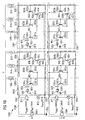
- Fig.1 1 schematically shows a sensor arrangement 100 according to the prior art with four sensor devices 101 to 104, a multiplexer shown as switch 105 and a readout circuit 106.
- the outputs of the individual sensor devices are read out using the multiplexer 105, that is serial.
- the respective sensor device 101 to 104 coupled to the read-out circuit 106 via the multiplexer 105 outputs an output voltage correlated with the event to be detected (for example, the illumination intensity in a photosensor or an electrical signal of a nerve cell arranged on the respective sensor device) ,
- the sensor devices 101 to 104 are shown schematically as voltage sources V 1 , V 2 , V 3 , V 4 .
- the first sensor device 101 is coupled to the read-out circuit 106 via the multiplexer 105.
- the readout circuit 106 By means of the readout circuit 106, the output voltage of a respective Sensor device 101 to 104 reinforced for further processing.
- Fig.2 shown sensor assembly 200 shows in addition to the in Fig.1 components described an internal resistance R i 201 of each of the sensor devices and a common capacitance C 202 of the sensor devices 101 to 104.
- the time constant ⁇ RC is a characteristic measure of the minimum achievable time between two consecutive measurements. Therefore, the value of ⁇ results in a limitation of the maximum number of sensor devices that can be read out within a predetermined period of time at a given sampling rate.
- the signal profile has fallen below the predetermined tolerable value V tol for the first time.
- the temporal signal profile at the in Fig.1, Fig.2 shown schematically voltage sources V 1 to V 4 .
- Waveform curve 303 reflects transient response across capacitance 202 and resistors R i , respectively, and is a good approximation of a falling exponential function.
- the dynamic error has dropped below the tolerable error for the first time, so that the at least required measuring time t is 0 .
- the sensor devices of a sensor array are read out in the voltage range, that is to say that the measured variable is converted into an electrical voltage.
- the RC constant low, and therefore to allow sufficiently fast readout of a sufficient number of sensor devices, an attempt is made to reduce the internal resistance R i and as a consequence the time constant ⁇ .
- an output driver circuit 400 is shown in which a MOS transistor 401 is operated in source circuit.
- the sensor device is shown as voltage source V G 402. Further, in the output driver circuit 400, there is shown a constant current source I 0 403, an ohmic resistor R 404 representing the internal resistance of the sensor device, and a capacitance C 405 representing the capacitance of a sensor device.
- the output voltage V out is applied to the capacitor 405.
- the voltage source 402 is coupled to the gate terminal of a MOS transistor 401.
- One source / drain terminal of the MOS transistor 401 is coupled to ground potential 407, whereas the other source / drain terminal of the MOS transistor 401 is coupled to both the constant current source 403 and the ohmic resistor 404 and the capacitor 405 is.
- the operating point of the MOS transistor 401 is determined by means of the constant current source 403, the ohmic resistor 404 and the voltage source V G 402.
- FIG 4B is a small signal equivalent circuit diagram 410 of FIG 4A shown output driver circuit 400.
- a controlled current source 411 g m ⁇ V G
- an effective internal resistance 412 g ds + R -1
- the capacity 405 to be transferred are shown.
- G ds denotes the output conductance of the MOS transistor 401
- g m is the transconductance of the MOS transistor 401.
- the source of the output driver circuit 400 is via the DC component of the voltage source V G 402 at the gate terminal of the MOS transistor 401 and over the with the other source / drain terminal of the MOS transistor 401 coupled constant current source I 0 with the internal resistance R.
- constant current source I 0 403, only with a resistor R 404 is possible.
- output driver circuit 400 shown is applied to each terminal of the constant current source 403 and the ohmic resistor 404, a supply voltage 406, whereas a terminal of the voltage source 402, the source / drain terminal of the MOS transistor 401 and a terminal of the capacitor 405 on Ground potential are 407.
- the drain current I D of the MOS transistor 401 changes by g m ⁇ V G. This is done by means of the controlled current source 411 4B symbolizing the small signal equivalent circuit of the output driver circuit 400.
- the change of the output voltage ⁇ V out results from the changed voltage drop across the MOS transistor 401 and the effective resistor 412.
- Equation (1) Substituting transistor parameters typical of CMOS technology into Equation (1) results in a possible voltage gain by a factor of about ten to about fifty. As a result, signals of small amplitude after the first amplifier stage are amplified so that they are no longer significantly disturbed by noise effects.
- the capacity is predetermined by the technology used and can therefore only be influenced to a very limited extent, for example by optimizing the layout.
- the parameters R and g ds can not be varied arbitrarily for a given gain and due to area restrictions, so that a limit for the maximum transferable bandwidth results from these boundary conditions.
- FIG.5A Another output driver circuit 500 according to the prior art described.
- FIG.5B is an equivalent circuit 510 of the in 5A shown output driver circuit 500 described.
- Those components of the output driver circuit 500 which are also included in the output driver circuit 400 are given the same reference numerals.
- the MOS transistor 401 is configured in source follower circuit. Notwithstanding the in 4A Output driver circuit 400 shown is that source / drain terminal of MOS transistor 401 that does not interfere with the Constant current source 403, the voltage source 402 and the capacitor 405 is coupled, at the potential of the supply voltage 406. Further, in the output driver circuit 500, a terminal of the constant current source 403 and the capacitor 405 at the electrical ground potential 407th Die Konstantstrom provoke I 0 403 and Voltage source V G 402 determine the operating point of the MOS transistor 401.
- the electrical current at the coupled with the constant current source I 0 403 source / drain terminal of the MOS transistor 401 is determined by the constant current source I 0 403rd
- the gate voltage of the MOS transistor 401 is set by means of the voltage source V G 402. Further, a capacity to be reloaded C 405 is shown.
- small signal equivalent circuit diagram 510 of FIG.5B is a controlled current source g m ( ⁇ V G - ⁇ V out ) 511 and an internal resistance g ds shown.
- small signal equivalent circuit diagram 510 is based on the field effect modulation of the electric current in accordance with 5A lower source / drain terminal of the MOS transistor 401 as a controlled current source g m (.DELTA.V G -V out ) 511 shown.
- the time constant ⁇ C from equation (3) corresponds to the scenario of the source circuit of the MOS transistor 401 4A if the value of the ohmic resistance R is equal to the inverse steepness g m -1 of the MOS transistor 401 (cf.
- This low gain is disadvantageous because of the small signal amplitudes that must be passed out of the sensor device, as noise effects can corrupt the measured signal.
- a gas detection device which has a transistor as a detection element.
- sensors with chemically sensitive field effect transistors are described, which have membranes on the gate insulation layer.
- the invention is based on the problem to provide a sensor arrangement with high spatial resolution, which at a sufficiently high signal amplification, a fast reading of sensor signals, i. a high bandwidth, and which is independent of parameter variations of their electronic components.
- the sensor arrangement according to the invention contains a plurality of sensor devices formed on and / or in a substrate.
- Each sensor device has an electrical signal converter and a sensor element coupled to the signal converter, with which the electrical conductivity of the signal converter as a result of a sensor event on the sensor element can be influenced in a characteristic manner.
- the sensor device according to the invention has a device for keeping constant an applied voltage to the signal converter.
- each sensor device has means for detecting the value of the electric current flowing through the signal converter as a sensor signal.
- the electrical signal converter is a field-effect transistor whose gate terminal is coupled to the sensor element, wherein the means for keeping constant an electrical Voltage is arranged such that it keeps constant the electrical voltage between the source / drain terminals of the field effect transistor.
- the sensor arrangement has a calibration device of a respective sensor device, which is set up in such a way that the gate region of the field effect transistor can be brought to such an electrical calibration potential that the electric current is independent of parameter fluctuations of the field effect transistor is.
- a method for operating a sensor arrangement having the abovementioned features, wherein, according to the method, the electrical conductivity of the signal converter is influenced in a characteristic manner as a result of a sensor event on a respective sensor element. Furthermore, the voltage at the signal converter is kept constant. The electrical current flowing through the signal converter is detected as a sensor signal. At least some of the sensor devices are calibrated by bringing the gate region of the respective field effect transistor to such an electrical calibration potential that the value of the electrical current during a sensor event is independent of parameter fluctuations of the field effect transistor.
- a basic idea of the invention is based on detecting an electric current instead of the electrical voltage on a signal converter coupled to the sensor element.
- an electric current and not, as in the prior art, an electrical voltage is detected, a transfer of capacity is avoided.
- a larger bandwidth that is, a faster readout of the sensor elements of a sensor arrangement allows.
- the time constant of the system is no longer determined by the interconnection within the sensor device, but only by the external Circuit.
- the electrical voltage is externally stabilized as a sensor signal.
- circuit architecture according to the invention for a sensor arrangement a particularly high number of sensor elements and a particularly high sampling rate are possible with a given technology, whereby a small time constant for reading out the sensor elements is achieved. Due to the interconnection of the sensor device according to the invention, an electrical sensor current is detected instead of an electrical sensor voltage, which leads to a high gain and a small time delay.
- an output driver circuit of a sensor device is implemented in a "current-mode technique".
- the sensor arrangement according to the invention is integrated Circuit, for example, in and / or on a silicon substrate (eg wafer, chip, etc.) realized. This achieves miniaturization and thus creates an array with a high number of sensor devices. Furthermore, the sensor assembly can be manufactured at a reasonable cost using modern and sophisticated silicon microtechnology.
- the electronic signal converter is a field-effect transistor whose gate terminal is coupled to the sensor element, wherein the device for keeping an electrical voltage constant is set up in such a way that it measures the electrical voltage between the source / drain Terminals of the field effect transistor keeps constant.
- a field effect transistor as a signal converter has the functionality that a modulation of the gate voltage is converted into a changed electrical conductivity of the channel region of the field effect transistor, so that the value of the current flowing through a source / drain terminal due to the changed ohmic resistance of the channel region of the field effect transistor is influenced characteristically.
- the sensor device may have an evaluation unit, wherein the evaluation unit, the value of the electric current is provided as a sensor signal.
- the evaluation unit is preferably set up in such a way that it forms an electrical voltage characteristic of this value from the value of the electrical current or maps the value of the electrical current to a digitally coded value characterizing this value.
- the detected electric current can be converted into an electrical voltage, which can be advantageous for the further processing of the signal.
- an analog current signal can be converted into a digital and thus error-robust signal.
- the evaluation unit can have an operational amplifier, in particular in a circuit as a voltage follower, which has a first input to which the sensor signal can be applied. Furthermore, the operational amplifier has a second input, to which an electrical reference potential can be applied. At an output of the operational amplifier, the characteristic electrical voltage is provided, wherein the first input and the output are coupled together by means of an ohmic resistor.
- the sensor arrangement can be designed as a biosensor arrangement.
- the sensor element of each sensor device can detect, for example, an electrical signal of a nerve cell grown on the sensor element.
- the sensor element may detect electrically charged particles on the sensor element using an ISFET.
- the sensor arrangement has a calibration device for calibrating a respective sensor device, which is set up in such a way that the gate region of the field effect transistor can be brought to such an electrical calibration potential that the electrical current of parameter fluctuations of the field effect transistor is independent.
- a calibration device for calibrating a respective sensor device, which is set up in such a way that the gate region of the field effect transistor can be brought to such an electrical calibration potential that the electrical current of parameter fluctuations of the field effect transistor is independent.
- field effect transistors of different sensor devices may have different parameters (e.g., threshold voltage).
- the calibration can be used to ensure that parameter fluctuations do not lead to a falsification when detecting a sensor event.
- the sensor device can be calibrated to provide a robust sensor arrangement. Signal influencing due to parameter fluctuations of the components of a respective sensor device, for example the signal converter implemented as field-effect transistors, is thereby avoided.
- the calibration device can be set up such that an electrical calibration current can be applied for calibration to the gate terminal and to a source / drain terminal of the field effect transistor.
- the evaluation unit may comprise a correllated double sampling device, which is set up in such a way that, in the event of a sensor event, it forms a value of the electrical current independent of parameter fluctuations of a respective field effect transistor.
- a sensor event in a sensor device is clearly detected in a first step and the sensor signal is stored.
- This sensor signal is dependent on the change in the value of the physical parameters of the sensor device (for example, geometric parameters of a field effect transistor) and may also be dependent on physical parameters of other components, for example an amplifier for amplifying the sensor signal.
- an auxiliary signal is detected, which depends only on the value of the physical parameter of the sensor device. If the auxiliary signal is subtracted from the sensor signal, a sensor signal substantially independent of the value of the physical parameter is obtained.
- the correlated double sampling device of the invention can be set up in such a way that in a calibration phase the gate region of the field effect transistor is brought to an electrical calibration potential, and the associated value of the electrical current is detected as the calibration signal and is stored.
- a detection phase the value of the electrical current due to a sensor event can be detected as a sensor signal.
- an evaluation phase the sensor signal and the calibration signal can be evaluated together.
- the sensor devices of the sensor arrangement are substantially arranged in matrix form in and / or on the substrate , and are interconnected by means of row and column lines such that the sensor devices can be controlled individually, line by line or column by column.
- At least one evaluation unit, at least one calibration device and / or at least one correlated double-sampling device can be provided for at least part of the sensor devices a row line or a column line may be provided together.
- the inventive method can be used as an electronic signal converter of a respective sensor array, a field effect transistor whose gate terminal is coupled to the sensor element, wherein means of the means for keeping a constant voltage, the electrical voltage between the source / drain Terminals of the field effect transistor is kept constant.
- a respective sensor device can be calibrated by bringing the gate region of the field effect transistor to such an electrical calibration potential that the value of the electrical current in the event of a sensor event is dependent on the properties of the field effect transistor (eg a production-related deviation of the thickness the gate insulating layer becomes independent of a desired or average value).
- a value of the electric current independent of the characteristics of the field effect transistor can be formed during a sensor event.
- Sensor device 600 shown has a field effect transistor 601 as an electrical signal converter. Furthermore, the sensor device 600 has a biosensor element coupled to the field effect transistor 601, this in Figure 6 is shown schematically as a voltage source 602. If a sensor event occurs at the biosensor element, the electrical conductivity of the channel region of the field effect transistor 601 is influenced in a characteristic manner as a result of this sensor event.
- a first source / drain terminal 601a of the field effect transistor 601 is coupled to one terminal of an ammeter 603 for detecting a sensor current I out , to whose other terminal a supply voltage 604 is applied.
- a second source / drain terminal 601b of the field effect transistor 601 is at the ground potential 605. Due to this connection, a constant electric potential difference is applied between the source / drain terminals 601a, 601b.
- a capacitor 606 representing the effective capacitance of the sensor device 600 also has the constant voltage V out resulting from the difference between the supply voltage 604 and the ground potential 605.
- the ammeter 603 is a device for detecting the value of the electric current flowing through the first source / drain terminal 601a of the field effect transistor 601 as a sensor signal.
- the gate terminal 601 c of the field effect transistor 601 is coupled to the voltage source 602.
- the electric voltage between the source / drain terminals 601a, 601b of the field effect transistor 601 is constant.
- the first source / drain terminal 601 a of the field effect transistor 601 is coupled to one terminal of the capacitor 606 and is further coupled to the ammeter 603.
- the electrical voltage V G of the voltage source 602 is thereby modulated. This is provided at the gate terminal 601 c of the field effect transistor 601, so that the electrical conductivity of the channel region of the Field effect transistor 601 is thereby influenced characteristically. Thereby, the value of the electric current flow through the source / drain terminal 601a of the field effect transistor 601, which current flow is detected by the ammeter 603, is a characteristic measure of the sensor event.
- the field effect transistor 601 is operated in "current mode".
- the voltage source 602 V G determines the potential applied to the gate region 601c, whereas the voltage at the first source / drain terminal 601a is fixed to the supply voltage 604.
- the output current I out is detected. It should be noted that the capacitor C 606 does not have to be reloaded because the voltage is kept constant.
- the evaluation unit has the functionality to keep the electrical voltage on a sensor line constant and simultaneously convert the detected sensor current (preferably linear) into a sensor voltage. This allows further processing in the voltage range.
- evaluation unit 700 shows an embodiment with which it is possible to convert a current signal .DELTA.I meas into a voltage signal .DELTA.V out .
- Z is the value of a resistor 701.
- the modulated value of the electrical current ⁇ I meas is provided as the sensor signal at an input 702 of the evaluation unit 700.
- the evaluation unit 700 has an operational amplifier 703.
- the operational amplifier 703 has a non-inverting input 703a at which the sensor signal ⁇ I meas is provided. Furthermore, the operational amplifier 703 has a non-inverting input 703b, to which a constant reference electrical potential V kal is applied.
- the characteristic electrical voltage .DELTA.V out is provided at an output 703c of the operational amplifier 703, the characteristic electrical voltage .DELTA.V out is provided.
- the output 703c of the operational amplifier 703 is fed back to the inverting input 703a of the operational amplifier 703 via the resistor Z701.
- the electrical potential V kal is provided at the non-inverting input 703b of the operational amplifier 703 by means of the constant voltage source 704.
- the constant voltage source 704 is connected between the ground electrical potential 605 and the non-inverting input 703b of the operational amplifier 703.
- the sensor arrangement 800 has a multiplicity of sensor devices 801 arranged in the form of a matrix, which are interconnected by means of row and column lines in such a way that the sensor devices 801 can be controlled individually or in columns.
- the sensor devices 801 of the sensor arrangement 800 are formed on and in a silicon substrate (not shown). In other words, the sensor arrangement 800 is realized as an integrated circuit.
- FIGS Figure 8 For the purpose of a simplified illustration, only the nth and (n + 1) th column of sensor devices 801 and the mth and (m + 1) th lines of the sensor devices 801 are shown.
- a sensor element 801 of the sensor arrangement 800 is in Figure 8 shown schematically as a voltage source 802, which is arranged between the ground potential 605 and a terminal of a capacitor 803.
- the capacitor 803 symbolizes a dielectric applied to the sensor element, which spatially decouples electrically charged particles to be detected thereon from the gate region 804c of a detection transistor 804.
- the other terminal of the capacitor 803 is further coupled to the first source / drain terminal 805a of a calibration transistor 805.
- the second source / drain terminal 805b of the calibration transistor 805 is coupled to the first source / drain terminal 804a of the sense transistor 804.
- the first source / drain terminal 804a of the sense transistor 804 is coupled to the first source / drain terminal 806a of a select transistor 806.
- the second source / drain terminal 806b of the select transistor 806 is coupled to a switch element 807 which is common to each row of sensor devices 801.
- the gate terminal 806c of the select transistor 806 is coupled to a first column line 808 that is common to each column of sensor devices 801.
- the second source / drain terminal 804b of the sense transistor 804 is coupled to a row line 809 which is common to each row of sensor devices 801.
- the switching element 807 may be connected in one of two switch positions "a" and "b", respectively, depending on whether a calibration mode or a measurement mode should be set.
- the switch element 807 is in the "b" position such that the second source / drain terminal 806b of the select transistor 806 is coupled to a calibration constant current source 810.
- the switching element 807 is in the switch position "a" (not shown in the figure)
- the second source / drain terminal 806b of the selection transistor 806 is coupled to a sense constant voltage source 811.
- a current detection unit 812 ie for example an ammeter, the value of the electric current flowing on the row line 809 can be detected.
- a select port 813 is coupled to the first column line 808. If an electrical signal having a logical value "1" is applied to the selection terminal 813, then all the selection transistors 806 of the associated column of sensor devices 801 are electrically conductive, so that the associated column is selected by sensor devices 801c. Furthermore, a calibration terminal 814 is in each case coupled to a respective second column line 815, wherein a common second column line 815 and a common calibration terminal 814 are provided for each column of sensor devices 801. If a signal with a logic value "1" is present at the calibration terminal 814, then all the calibration transistors 805 of the associated column of sensor devices 801 are electrically conductive, so that calibration is possible.
- the sensor devices 801 are column-calibrated in order to vary fluctuating characteristics between different sensor devices (for example, fluctuations in the value of the threshold voltage the sense transistors 804).
- To calibrate the n-th column it is activated as a single column by applying a control signal of logic "1" to the selection port 813 of the n-th column of sensor devices 801.
- At the select terminals 813 of all other columns of sensor devices 801 is a signal with a logic value "0".
- the channel regions of all select transistors 806 of the nth column of sensor devices 801 are electrically conductive, whereas the select transistors 806 of all other columns of sensor devices 801 are nonconductive.
- This voltage is different for each sensor device 801 of the n-th column of sensor devices 801, since the electrical parameters of the detection transistor 804 may vary due to statistical effects.
- the signal at the calibration terminal 814 is brought to a logical value "0" , is illustratively associated with the electrical current value I kal associated electrical gate voltage stored at the gate terminal 804c of the detecting transistor 804. This calibration procedure is repeated step by step for all columns.
- the switching element 807 is switched to the switch position "a" (not shown in FIG Figure 8 ).
- the constant voltage V drain is impressed into all the circuit means 801 of an associated row of circuit devices 801 using the detection constant voltage source 811.
- the sensor arrangement 800 is read out in columns sequentially. A column to be read is selected by bringing the associated select terminal 813 to an electrical potential of logic "1" so that all the select transistors 806 of the associated column of sensor arrays 801 are brought into an electrically conductive state. If no sensor event occurs at a sensor element of a sensor device 801 of a selected column of sensor devices 801, the DC component which flows through the activated sensor device 801 flows on the gate connection 804c of the detection transistor 804 was stored in the calibration phase.
- the output is the same for an identical sensor event and does not depend on the varying parameters of the transistors. If, as a result of a sensor event, a modulation of the electrical potential on a sensor element results, a modulation of the electrical voltage at the gate terminal 804c of the associated detection transistor 804 and consequently the electrical current at the first source / drain Terminal 804a of sense transistor 804. This modulation is detected by current sense unit 812 and can be amplified by external amplifier elements. Optional can the electrical sensor current signal is converted into an electrical voltage (see evaluation unit 700 from Fig. 7 ).
- the sensor devices 801 can be activated or deactivated in columns.
- a sensor signal is amplified or converted into an electrical current.
- calibrating the sensor devices 801 statistical fluctuations of parameters of the sensor devices 801 are compensated.
- FIG 9 a sensor arrangement 900 according to a second preferred embodiment of the invention described.
- sensor assembly 900 is a modification of in Figure 8 shown sensor assembly 800.
- the same or similar components are therefore provided with the same reference numerals.
- the essential difference between the sensor arrangement 900 and the sensor arrangement 800 is that in the case of the sensor devices 901 of the sensor arrangement 900, the calibration transistor 805 is connected in a modified manner.
- the second source / drain terminal 805b of the calibration transistor 805 is coupled to the second source / drain terminal 806b of the select transistor 806 and directly to the row line 809.
- the calibration transistor 805 of the sensor array 900 coupled directly to the row line 809 (illustratively readout line)
- the parasitic capacitance at the output node of a sensor arrangement 901 according to the sensor arrangement 900 may be somewhat higher, since in this case two transistors with their source / drain terminals are permanently on common output node of a sensor array 901 are connected to a line.
- FIG 10 a sensor arrangement 1000 according to a third preferred embodiment of the invention described. Those components of the sensor arrangement 1000 which also occur in the sensor arrangement 800 or 900 are provided with the same reference numbers.
- the sensor arrangement 1000 is a matrix-like arrangement of a plurality of sensor devices 1005.
- a sensor element of a sensor device 1005 is symbolized as a voltage source 802, which according to Figure 10 are connected between a terminal at electrical ground potential and the capacitor 803.
- the capacitor 803 represents a dielectric layer on the sense transistor 804, by means of which the sensor element 802 is decoupled from the sense transistor 804.
- the capacitor 803 is coupled to the first source / drain terminal 1001a of a switching transistor 1001.
- the second source / drain terminal 1001 b of the switching transistor 1001 is coupled to the first source / drain terminal 805 a of the calibration transistor 805 and to the gate terminal 804 c of the detection transistor 804.
- the gate terminal 1001c of the switching transistor 1001 is coupled to a switching terminal 1002 via a third column line 1003.
- a separate third column line 1003 is provided for each column of sensor devices 1005.
- the first source / drain terminal 804a of the sense transistor 804 is coupled to the first source / drain terminal 806a of the select transistor 806, whose gate terminal 806b is coupled to the select terminal 813 via the first column line 808 ,
- the gate terminal 805c of the calibration transistor 805 is coupled to the calibration terminal 814 via the second column line 815.
- the second source / drain connection 805b of the calibration transistor 805 is coupled to a first row line 1006, which is common to each row of sensor devices 1005.
- the first row line 1006 is coupled to a calibration constant voltage source 1004.
- the second source / drain terminal 806b of the select transistor 806 is coupled via a second row line 1007 to the sense constant voltage source 811, which in turn is coupled to the current sense unit 812.
- the current detection unit 812 is coupled to the calibration constant voltage source 1004.
- the sensor devices 1005 can be activated or deactivated column by column.
- the sensor signal or a reference signal can be amplified or converted into an electrical current.
- the sensor device 1000 is suitable for Correlated Double Sampling for eliminating parameter fluctuations.
- n-MOS transistors 1001, 805, 806 coupled to one of the column lines 1003, 815 and 808, respectively, by applying an electrical signal having a logical value "1" to the associated terminal 1002, 814 or 813 can be brought into an electrically conductive state and thus represent a negligibly small ohmic resistance. If, however, the electrical signal to an associated terminal 1002, 814 or 813 is at a logical value "0", then the driven transistor is non-conductive, wherein the leakage currents of the field effect transistors can be neglected.
- the sensor arrangement 1000 is based on the Correlated Double Sampling principle (CDS method), which suppresses parameter fluctuations and low-frequency noise become.
- CDS method a reference signal is usually applied to an input of an amplifier first. At the output of the amplifier then the amplified reference signal plus an offset signal of the amplifier is stored. In a next phase, the sensor signal is applied to the amplifier. At the output of the amplifier is then the amplified measurement signal including the offset signal. By differentiating the two values it is possible to eliminate the offset signal of the amplifier.
- the sensor devices 1005 of the sensor arrangement 1000 are read out in columns sequentially.
- One column (eg, the nth column) of sensor devices 1005 is activated by setting the selection port 813, the first column line 808, and hence the gate terminals 806c of the select transistors 806 of the associated column to a logical value "1" are brought.
- the pixels of a column are read out according to the embodiment in two phases.
- the reference voltage V kal of the calibration constant voltage source 1004 in an associated sensor arrangement 1005 is converted into an electric current and its value is detected.
- an electrical signal having a logic value "1" is applied to the calibration terminal 814, so that the calibration transistors 805 coupled thereto via the second column line 815 are brought into an electrically conductive state.
- the switching terminal 1002 in this phase is at a logical value "0", so that the switching transistor 1001 is electrically non-conductive.
- the reference voltage V kal is applied , resulting in a corresponding electric current through the first source / drain terminal 804a of the detecting transistor 804.
- the value of this electrical current may be due to statistical variations of transistor parameters for different sensor devices 1005 of the sensor array 1000 be different.
- the value of this electrical current is detected and stored in the readout circuit of the respective row as electrical reference current I meas (m).
- the actual sensor signal is detected.
- the electrical signal at the calibration terminal 814 is brought to a logic value "0", whereby the calibration transistors 805 block.
- an electric signal having a logical value "1" is applied to the switching terminal 1002, so that the switching transistors 1001 are brought into an electrically conductive state.
- This mimics a change in the electrical potential on the sensor element 802 on the gate terminal 804c of the sense transistor 804, resulting in a modulation of the electrical current through the first source / drain terminal 804a of the sense transistor 804.
- the value of this electric current is detected, then the difference between the detected current values from the first and the second phase is formed.
- parameter fluctuations between the different sensor devices are suppressed and the output signal obtained depends exclusively on the sensor event.
Landscapes
- Health & Medical Sciences (AREA)
- Life Sciences & Earth Sciences (AREA)
- Chemical & Material Sciences (AREA)
- Molecular Biology (AREA)
- Physics & Mathematics (AREA)
- Analytical Chemistry (AREA)
- General Health & Medical Sciences (AREA)
- Engineering & Computer Science (AREA)
- Chemical Kinetics & Catalysis (AREA)
- Electrochemistry (AREA)
- Spectroscopy & Molecular Physics (AREA)
- Biochemistry (AREA)
- Microelectronics & Electronic Packaging (AREA)
- General Physics & Mathematics (AREA)
- Immunology (AREA)
- Pathology (AREA)
- Measurement Of Current Or Voltage (AREA)
- Semiconductor Integrated Circuits (AREA)
- Transforming Light Signals Into Electric Signals (AREA)
- Electronic Switches (AREA)
Applications Claiming Priority (3)
| Application Number | Priority Date | Filing Date | Title |
|---|---|---|---|
| DE10247889 | 2002-10-14 | ||
| DE10247889A DE10247889A1 (de) | 2002-10-14 | 2002-10-14 | Sensor-Anordnung und Verfahren zum Betreiben einer Sensor-Anordnung |
| PCT/EP2003/011381 WO2004036203A1 (de) | 2002-10-14 | 2003-10-14 | Sensor-anordnung und verfahren zum betreiben einer sensor-anordnung |
Publications (2)
| Publication Number | Publication Date |
|---|---|
| EP1554569A1 EP1554569A1 (de) | 2005-07-20 |
| EP1554569B1 true EP1554569B1 (de) | 2008-06-11 |
Family
ID=32038670
Family Applications (1)
| Application Number | Title | Priority Date | Filing Date |
|---|---|---|---|
| EP03772214A Expired - Fee Related EP1554569B1 (de) | 2002-10-14 | 2003-10-14 | Sensor-anordnung und verfahren zum betreiben einer sensor-anordnung |
Country Status (5)
| Country | Link |
|---|---|
| US (1) | US7662341B2 (ja) |
| EP (1) | EP1554569B1 (ja) |
| JP (1) | JP4351632B2 (ja) |
| DE (1) | DE10247889A1 (ja) |
| WO (1) | WO2004036203A1 (ja) |
Families Citing this family (52)
| Publication number | Priority date | Publication date | Assignee | Title |
|---|---|---|---|---|
| DE102004023855B4 (de) * | 2004-05-13 | 2006-11-30 | Infineon Technologies Ag | Schaltkreis-Anordnung |
| EP1756563A1 (en) * | 2004-06-12 | 2007-02-28 | Akubio Limited | Analytical apparatus with array of sensors and calibrating element |
| CN101006338A (zh) * | 2004-10-14 | 2007-07-25 | 株式会社东芝 | 基于fet的核酸探测传感器 |
| DE102005006772A1 (de) * | 2005-02-15 | 2006-08-24 | Vogt Electronic Components Gmbh | Sensorelement mit Verbindungsleitung |
| US7549795B2 (en) * | 2006-06-30 | 2009-06-23 | Intel Corporation | Analog thermal sensor array |
| US8129978B2 (en) | 2006-07-13 | 2012-03-06 | National University Corporation Nagoya University | Material detector |
| US8349167B2 (en) | 2006-12-14 | 2013-01-08 | Life Technologies Corporation | Methods and apparatus for detecting molecular interactions using FET arrays |
| EP2674751B1 (en) | 2006-12-14 | 2017-02-01 | Life Technologies Corporation | Apparatus for measuring analytes using large scale FET arrays |
| US8262900B2 (en) | 2006-12-14 | 2012-09-11 | Life Technologies Corporation | Methods and apparatus for measuring analytes using large scale FET arrays |
| US11339430B2 (en) | 2007-07-10 | 2022-05-24 | Life Technologies Corporation | Methods and apparatus for measuring analytes using large scale FET arrays |
| KR101176547B1 (ko) | 2006-12-20 | 2012-08-24 | 리전츠 오브 더 유니버스티 오브 미네소타 | 잡음이 감소된 이온 물질 검출 장치 및 방법 |
| EP2982437B1 (en) | 2008-06-25 | 2017-12-06 | Life Technologies Corporation | Methods and apparatus for measuring analytes using large scale fet arrays |
| US8262879B2 (en) | 2008-09-03 | 2012-09-11 | Nabsys, Inc. | Devices and methods for determining the length of biopolymers and distances between probes bound thereto |
| US9650668B2 (en) | 2008-09-03 | 2017-05-16 | Nabsys 2.0 Llc | Use of longitudinally displaced nanoscale electrodes for voltage sensing of biomolecules and other analytes in fluidic channels |
| US20100137143A1 (en) | 2008-10-22 | 2010-06-03 | Ion Torrent Systems Incorporated | Methods and apparatus for measuring analytes |
| US20100301398A1 (en) | 2009-05-29 | 2010-12-02 | Ion Torrent Systems Incorporated | Methods and apparatus for measuring analytes |
| CN103884760A (zh) * | 2008-10-22 | 2014-06-25 | 生命技术公司 | 单芯片化学测定装置和单芯片核酸测定装置 |
| US8776573B2 (en) | 2009-05-29 | 2014-07-15 | Life Technologies Corporation | Methods and apparatus for measuring analytes |
| US20120261274A1 (en) | 2009-05-29 | 2012-10-18 | Life Technologies Corporation | Methods and apparatus for measuring analytes |
| DE102009043527B4 (de) * | 2009-09-30 | 2021-06-10 | Boehringer Ingelheim Vetmedica Gmbh | Anordnung und Verfahren unter Verwendung von Mikrosensoren zum Messen von Zell-Vitalitäten |
| DE102009045475B4 (de) * | 2009-10-08 | 2023-06-29 | Robert Bosch Gmbh | Gassensitive Halbleitervorrichtung sowie deren Verwendung |
| JP2013533482A (ja) | 2010-06-30 | 2013-08-22 | ライフ テクノロジーズ コーポレーション | イオン感応性電荷蓄積回路および方法 |
| WO2012003359A1 (en) | 2010-06-30 | 2012-01-05 | Life Technologies Corporation | Methods and apparatus for testing isfet arrays |
| CN114019006A (zh) * | 2010-06-30 | 2022-02-08 | 生命科技公司 | 阵列列积分器 |
| US11307166B2 (en) | 2010-07-01 | 2022-04-19 | Life Technologies Corporation | Column ADC |
| US8653567B2 (en) | 2010-07-03 | 2014-02-18 | Life Technologies Corporation | Chemically sensitive sensor with lightly doped drains |
| US8373206B2 (en) * | 2010-07-20 | 2013-02-12 | Nth Tech Corporation | Biosensor apparatuses and methods thereof |
| US9618475B2 (en) | 2010-09-15 | 2017-04-11 | Life Technologies Corporation | Methods and apparatus for measuring analytes |
| US8685324B2 (en) | 2010-09-24 | 2014-04-01 | Life Technologies Corporation | Matched pair transistor circuits |
| EP2640849B1 (en) | 2010-11-16 | 2016-04-06 | Nabsys 2.0 LLC | Methods for sequencing a biomolecule by detecting relative positions of hybridized probes |
| US9970984B2 (en) | 2011-12-01 | 2018-05-15 | Life Technologies Corporation | Method and apparatus for identifying defects in a chemical sensor array |
| US8786331B2 (en) | 2012-05-29 | 2014-07-22 | Life Technologies Corporation | System for reducing noise in a chemical sensor array |
| US9914966B1 (en) * | 2012-12-20 | 2018-03-13 | Nabsys 2.0 Llc | Apparatus and methods for analysis of biomolecules using high frequency alternating current excitation |
| US9080968B2 (en) | 2013-01-04 | 2015-07-14 | Life Technologies Corporation | Methods and systems for point of use removal of sacrificial material |
| US9841398B2 (en) | 2013-01-08 | 2017-12-12 | Life Technologies Corporation | Methods for manufacturing well structures for low-noise chemical sensors |
| US10294516B2 (en) | 2013-01-18 | 2019-05-21 | Nabsys 2.0 Llc | Enhanced probe binding |
| US8962366B2 (en) | 2013-01-28 | 2015-02-24 | Life Technologies Corporation | Self-aligned well structures for low-noise chemical sensors |
| US8963216B2 (en) | 2013-03-13 | 2015-02-24 | Life Technologies Corporation | Chemical sensor with sidewall spacer sensor surface |
| US8841217B1 (en) | 2013-03-13 | 2014-09-23 | Life Technologies Corporation | Chemical sensor with protruded sensor surface |
| US9835585B2 (en) | 2013-03-15 | 2017-12-05 | Life Technologies Corporation | Chemical sensor with protruded sensor surface |
| EP2972279B1 (en) | 2013-03-15 | 2021-10-06 | Life Technologies Corporation | Chemical sensors with consistent sensor surface areas |
| US9116117B2 (en) | 2013-03-15 | 2015-08-25 | Life Technologies Corporation | Chemical sensor with sidewall sensor surface |
| WO2014149779A1 (en) | 2013-03-15 | 2014-09-25 | Life Technologies Corporation | Chemical device with thin conductive element |
| CN105264366B (zh) | 2013-03-15 | 2019-04-16 | 生命科技公司 | 具有一致传感器表面区域的化学传感器 |
| US20140336063A1 (en) | 2013-05-09 | 2014-11-13 | Life Technologies Corporation | Windowed Sequencing |
| US10458942B2 (en) | 2013-06-10 | 2019-10-29 | Life Technologies Corporation | Chemical sensor array having multiple sensors per well |
| JP6154011B2 (ja) * | 2013-06-27 | 2017-06-28 | 株式会社日立製作所 | 半導体装置およびその製造方法 |
| US10077472B2 (en) | 2014-12-18 | 2018-09-18 | Life Technologies Corporation | High data rate integrated circuit with power management |
| US10379079B2 (en) | 2014-12-18 | 2019-08-13 | Life Technologies Corporation | Methods and apparatus for measuring analytes using large scale FET arrays |
| KR102593647B1 (ko) | 2014-12-18 | 2023-10-26 | 라이프 테크놀로지스 코포레이션 | 트랜스미터 구성을 갖춘 높은 데이터율 집적 회로 |
| KR101760511B1 (ko) * | 2016-12-07 | 2017-07-21 | 주식회사 유메딕스 | 환경 센서 신호 검출 회로, 바이오 센서 신호 검출 회로 및 이들을 포함하는 이종 센서 인터페이스 |
| EP4081793A1 (en) * | 2019-12-24 | 2022-11-02 | Università degli Studi di Bari "Aldo Moro" | Transistor-based biological assay system comprising mating receptacle plate and gate electrode plate |
Family Cites Families (16)
| Publication number | Priority date | Publication date | Assignee | Title |
|---|---|---|---|---|
| US4322680A (en) | 1980-03-03 | 1982-03-30 | University Of Utah Research Foundation | Chemically sensitive JFET transducer devices utilizing a blocking interface |
| US4411741A (en) | 1982-01-12 | 1983-10-25 | University Of Utah | Apparatus and method for measuring the concentration of components in fluids |
| US4514263A (en) | 1982-01-12 | 1985-04-30 | University Of Utah | Apparatus and method for measuring the concentration of components in fluids |
| NL8600872A (nl) * | 1986-04-07 | 1987-11-02 | Sentron V O F | Veldeffecttransistor, voorzien van een de gateisolator bedekkend membraan. |
| CA1318353C (en) * | 1987-05-05 | 1993-05-25 | Peter Wing-Poon Cheung | System employing a biosensor to monitor a characteristic of a select component in a medium |
| US20010045508A1 (en) | 1998-09-21 | 2001-11-29 | Bart Dierickx | Pixel structure for imaging devices |
| US6011251A (en) | 1997-06-04 | 2000-01-04 | Imec | Method for obtaining a high dynamic range read-out signal of a CMOS-based pixel structure and such CMOS-based pixel structure |
| FI103617B1 (fi) | 1997-09-01 | 1999-07-30 | Nokia Mobile Phones Ltd | Kanavatransistorit |
| JP2000033712A (ja) * | 1997-09-30 | 2000-02-02 | Seiko Epson Corp | マイクロセンサーデバイス作成方法及びそれを用いた液体機能評価方法 |
| FR2779826B1 (fr) | 1998-06-12 | 2002-05-31 | Europhtal | Detecteur d'ozone, de dioxyde d'azote ou de tout autre gaz polluant et son utilisation |
| JP4137239B2 (ja) | 1998-08-03 | 2008-08-20 | 株式会社堀場製作所 | Isfetアレイ |
| US6321588B1 (en) * | 1998-09-11 | 2001-11-27 | Femtometrics, Inc. | Chemical sensor array |
| JP2002048108A (ja) * | 2000-08-04 | 2002-02-15 | Smc Corp | 位置検出センサの取付構造 |
| JP2002195997A (ja) | 2000-09-29 | 2002-07-10 | Toshiba Corp | 核酸検出用センサ |
| ATE303594T1 (de) | 2000-10-16 | 2005-09-15 | Infineon Technologies Ag | Elektronische schaltung, sensoranordnung und verfahren zum verarbeiten eines sensorsignals |
| DE10151020A1 (de) * | 2001-10-16 | 2003-04-30 | Infineon Technologies Ag | Schaltkreis-Anordnung, Sensor-Array und Biosensor-Array |
-
2002
- 2002-10-14 DE DE10247889A patent/DE10247889A1/de not_active Withdrawn
-
2003
- 2003-10-14 JP JP2004544228A patent/JP4351632B2/ja not_active Expired - Fee Related
- 2003-10-14 US US10/530,882 patent/US7662341B2/en not_active Expired - Fee Related
- 2003-10-14 WO PCT/EP2003/011381 patent/WO2004036203A1/de active IP Right Grant
- 2003-10-14 EP EP03772214A patent/EP1554569B1/de not_active Expired - Fee Related
Also Published As
| Publication number | Publication date |
|---|---|
| JP4351632B2 (ja) | 2009-10-28 |
| JP2006503279A (ja) | 2006-01-26 |
| DE10247889A1 (de) | 2004-04-22 |
| US20060057025A1 (en) | 2006-03-16 |
| WO2004036203A1 (de) | 2004-04-29 |
| EP1554569A1 (de) | 2005-07-20 |
| US7662341B2 (en) | 2010-02-16 |
Similar Documents
| Publication | Publication Date | Title |
|---|---|---|
| EP1554569B1 (de) | Sensor-anordnung und verfahren zum betreiben einer sensor-anordnung | |
| EP1272860B1 (de) | Sensor-anordnung und verfahren zum erfassen eines zustands eines transistors einer sensor-anordnung | |
| EP1405071B1 (de) | Messzelle zur aufnahme des elektrischen potentials einer probe | |
| EP1438571B1 (de) | Biosensor-schaltkreis und ein aus einer mehrzahl dieser biosensor-schaltkreise bestehender sensor-array und biosensor-array | |
| EP1516175B1 (de) | Biosensor-array und verfahren zum betreiben eines biosensor-arrays | |
| EP1436606B1 (de) | Sensor-anordnung | |
| EP0523463B1 (de) | Elektrochemisches Analysesystem | |
| DE112010002926B4 (de) | Elektrometer mit breitem Dynamikbereich und schneller Reaktion | |
| EP1715333B1 (de) | Verfahren zur Signalauslesung an einem gassensitiven Feldeffekttransistor | |
| DE102005027245A1 (de) | Schaltkreisanordnung | |
| EP1636599B1 (de) | Schaltkreisanordnung zur potentialkonstanthaltung an einem biosensor und zur digitalisierung des messstroms | |
| EP1525470A2 (de) | Sensor-anordnung | |
| DE10204652B4 (de) | Schaltkreis-Anordnung, elektrochemischer Sensor, Sensor-Anordnung und Verfahren zum Verarbeiten eines über eine Sensor-Elektrode bereitgestellten Stromsignals | |
| DE112015004384T5 (de) | Matrixvorrichtung, Verfahren zum Messen ihrer Eigenschaften und Betriebsverfahren derselben | |
| WO2005111978A1 (de) | Schaltkreis-anordnung | |
| DE3033730A1 (de) | Vorrichtung zum feststellen chemischer substanzen | |
| EP1484605A2 (de) | FET-sensor und Verfahren zum Ansteuern eines solchen FET-sensors | |
| DE102004025580A1 (de) | Sensor-Anordnung, Sensor-Array und Verfahren zum Herstellen einer Sensor-Anordnung | |
| EP2171441B1 (de) | Anordnung von Gassensoren | |
| DE60305865T2 (de) | DNA-spezifische Kapazitiver Affinitätssensor | |
| DE10228124A1 (de) | Biosensor-Array und Verfahren zum Betreiben eines Biosensor-Arrays | |
| EP1324054B1 (de) | Vorrichtung zur Messung der Stärke eines magnetischen Feldes, Magnetfeldsensor und Stromstärkemessgerät | |
| DE102005036288B4 (de) | Aktiver Tastkopf |
Legal Events
| Date | Code | Title | Description |
|---|---|---|---|
| PUAI | Public reference made under article 153(3) epc to a published international application that has entered the european phase |
Free format text: ORIGINAL CODE: 0009012 |
|
| 17P | Request for examination filed |
Effective date: 20050128 |
|
| AK | Designated contracting states |
Kind code of ref document: A1 Designated state(s): AT BE BG CH CY CZ DE DK EE ES FI FR GB GR HU IE IT LI LU MC NL PT RO SE SI SK TR |
|
| RBV | Designated contracting states (corrected) |
Designated state(s): FR GB |
|
| REG | Reference to a national code |
Ref country code: DE Ref legal event code: 8566 |
|
| GRAC | Information related to communication of intention to grant a patent modified |
Free format text: ORIGINAL CODE: EPIDOSCIGR1 |
|
| GRAP | Despatch of communication of intention to grant a patent |
Free format text: ORIGINAL CODE: EPIDOSNIGR1 |
|
| GRAS | Grant fee paid |
Free format text: ORIGINAL CODE: EPIDOSNIGR3 |
|
| GRAA | (expected) grant |
Free format text: ORIGINAL CODE: 0009210 |
|
| AK | Designated contracting states |
Kind code of ref document: B1 Designated state(s): FR GB |
|
| REG | Reference to a national code |
Ref country code: GB Ref legal event code: FG4D Free format text: NOT ENGLISH |
|
| PLBE | No opposition filed within time limit |
Free format text: ORIGINAL CODE: 0009261 |
|
| STAA | Information on the status of an ep patent application or granted ep patent |
Free format text: STATUS: NO OPPOSITION FILED WITHIN TIME LIMIT |
|
| 26N | No opposition filed |
Effective date: 20090312 |
|
| REG | Reference to a national code |
Ref country code: FR Ref legal event code: PLFP Year of fee payment: 13 |
|
| PGFP | Annual fee paid to national office [announced via postgrant information from national office to epo] |
Ref country code: GB Payment date: 20151021 Year of fee payment: 13 |
|
| PGFP | Annual fee paid to national office [announced via postgrant information from national office to epo] |
Ref country code: FR Payment date: 20151023 Year of fee payment: 13 |
|
| GBPC | Gb: european patent ceased through non-payment of renewal fee |
Effective date: 20161014 |
|
| REG | Reference to a national code |
Ref country code: FR Ref legal event code: ST Effective date: 20170630 |
|
| PG25 | Lapsed in a contracting state [announced via postgrant information from national office to epo] |
Ref country code: FR Free format text: LAPSE BECAUSE OF NON-PAYMENT OF DUE FEES Effective date: 20161102 Ref country code: GB Free format text: LAPSE BECAUSE OF NON-PAYMENT OF DUE FEES Effective date: 20161014 |