EP1554010B1 - Selektiv konfigurierbares multimodus-kristalloszillator-system zur minimierung des stromverbrauchs oder der geräuscherzeugung - Google Patents
Selektiv konfigurierbares multimodus-kristalloszillator-system zur minimierung des stromverbrauchs oder der geräuscherzeugung Download PDFInfo
- Publication number
- EP1554010B1 EP1554010B1 EP03773172A EP03773172A EP1554010B1 EP 1554010 B1 EP1554010 B1 EP 1554010B1 EP 03773172 A EP03773172 A EP 03773172A EP 03773172 A EP03773172 A EP 03773172A EP 1554010 B1 EP1554010 B1 EP 1554010B1
- Authority
- EP
- European Patent Office
- Prior art keywords
- crystal oscillator
- power supply
- frequency
- voltage
- series
- Prior art date
- Legal status (The legal status is an assumption and is not a legal conclusion. Google has not performed a legal analysis and makes no representation as to the accuracy of the status listed.)
- Expired - Lifetime
Links
- 239000013078 crystal Substances 0.000 title claims description 95
- 238000004891 communication Methods 0.000 claims description 42
- 239000003990 capacitor Substances 0.000 claims description 32
- 230000007423 decrease Effects 0.000 claims description 7
- 238000005259 measurement Methods 0.000 claims description 7
- 238000000034 method Methods 0.000 claims description 6
- 230000008878 coupling Effects 0.000 claims description 4
- 238000010168 coupling process Methods 0.000 claims description 4
- 238000005859 coupling reaction Methods 0.000 claims description 4
- 230000004044 response Effects 0.000 claims description 2
- 238000010586 diagram Methods 0.000 description 9
- 230000010355 oscillation Effects 0.000 description 4
- 239000004065 semiconductor Substances 0.000 description 3
- 238000012163 sequencing technique Methods 0.000 description 3
- 230000002457 bidirectional effect Effects 0.000 description 2
- 230000005540 biological transmission Effects 0.000 description 2
- 230000003247 decreasing effect Effects 0.000 description 2
- 230000002411 adverse Effects 0.000 description 1
- 230000008859 change Effects 0.000 description 1
- 230000000295 complement effect Effects 0.000 description 1
- 230000001351 cycling effect Effects 0.000 description 1
- 238000007599 discharging Methods 0.000 description 1
- 230000000694 effects Effects 0.000 description 1
- 230000005669 field effect Effects 0.000 description 1
- 235000003642 hunger Nutrition 0.000 description 1
- 238000002513 implantation Methods 0.000 description 1
- 238000009413 insulation Methods 0.000 description 1
- 238000012986 modification Methods 0.000 description 1
- 230000004048 modification Effects 0.000 description 1
- 238000012544 monitoring process Methods 0.000 description 1
- 230000003071 parasitic effect Effects 0.000 description 1
- 238000012545 processing Methods 0.000 description 1
- 239000007787 solid Substances 0.000 description 1
- 230000000638 stimulation Effects 0.000 description 1
- 239000000758 substrate Substances 0.000 description 1
- 230000002123 temporal effect Effects 0.000 description 1
Images


Classifications
-
- H—ELECTRICITY
- H03—ELECTRONIC CIRCUITRY
- H03L—AUTOMATIC CONTROL, STARTING, SYNCHRONISATION OR STABILISATION OF GENERATORS OF ELECTRONIC OSCILLATIONS OR PULSES
- H03L7/00—Automatic control of frequency or phase; Synchronisation
-
- Y—GENERAL TAGGING OF NEW TECHNOLOGICAL DEVELOPMENTS; GENERAL TAGGING OF CROSS-SECTIONAL TECHNOLOGIES SPANNING OVER SEVERAL SECTIONS OF THE IPC; TECHNICAL SUBJECTS COVERED BY FORMER USPC CROSS-REFERENCE ART COLLECTIONS [XRACs] AND DIGESTS
- Y10—TECHNICAL SUBJECTS COVERED BY FORMER USPC
- Y10S—TECHNICAL SUBJECTS COVERED BY FORMER USPC CROSS-REFERENCE ART COLLECTIONS [XRACs] AND DIGESTS
- Y10S323/00—Electricity: power supply or regulation systems
- Y10S323/911—Medical electronics
Definitions
- the present invention is generally directed to crystal oscillators and in particular to the use of crystal oscillators in applications that require low power consumption, e.g., a battery-powered implantable medical device, and applications that require low noise, e.g., communication systems, and systems for selectively achieving both low power consumption and low noise generation.
- low power consumption e.g., a battery-powered implantable medical device
- low noise e.g., communication systems, and systems for selectively achieving both low power consumption and low noise generation.
- the present invention relates to systems and in particular communication systems which require the use of a crystal oscillator for controlling communication rates and/or modulation.
- the crystal oscillator and/or a power supply for the crystal oscillator must have any noise generation be minimized to thus maximize the signal-to-noise ratio for the transmitted signal and to maximize the capability to detect and demodulate a low signal-to-noise level receive signal.
- a communication system resides in a battery-powered system, it additionally becomes desirable to minimize power consumption whenever possible.
- the battery-powered system is implantable and miniaturized, the need to minimize power consumption is further exacerbated.
- 6,164,284 entitled “System of Implantable Devices For Monitoring and/or Affecting Body Parameters” and U.S. Patent No. 6,185,452 entitled “Battery Powered Patient Implantable Device” describe devices configured for implantation within a patient's body, i.e., beneath a patient's skin, for performing various functions including: (1) stimulation of body tissue and/or sensing of body parameters, and (2) communicating between implanted slave devices and a master device which may be external to a patient's body.
- implantable devices are preferably powered from rechargeable batteries.
- the time between rechargings is potentially limited. Accordingly, power conservation techniques to extend the battery life of such devices are particularly desirable.
- the present invention is thus directed to a multi-mode crystal oscillator system selectively configurable to minimize power consumption or noise generation to thus achieve desired battery life and communication performances suitable for such an implantable device.
- JP59168704 discloses a semiconductor integrated circuit the purpose of which is to attain low power consumption and to decrease oscillation start time by using in common an oscillating circuit of a complementary insulation gate field effect semiconductor integrated circuit and a substrate bias circuit.
- JP61195388 discloses a timepiece device to deal with supply interruption by a charging type battery of a small capacity by alternatively and switchingly using a high precision oscillator operating by current supply from the battery.
- the present invention is directed to a multi-mode crystal oscillator system selectively configurable to minimize power consumption or noise generation.
- a system is particularly applicable to the communication system of an implantable device, e.g., the microstimulator/sensor device described in U.S. Patent Nos. 6,164,284 ; 6,185,452 ; 6,472,991 ; and the like.
- their small size an axial dimension of less than 60 mm and a lateral dimension of less than 6 mm limits the size of the battery contained within and thus makes it essential to minimize power consumption. Additionally, the small size and battery capacity result in a limited amount of transmission power.
- embodiments of the present invention alternatively supply power to a crystal oscillator in either a first mode that minimizes power consumption or a second mode that minimizes noise generation.
- a crystal oscillator system configured for alternatively minimizing power consumption or noise generation, comprises: (1) a crystal oscillator; (2) a first power supply for powering the crystal oscillator in a first mode of operation, wherein the first power supply operates as a switching downconverter to minimize power consumption; (3) a second power supply for powering the crystal oscillator in a second mode of operation, wherein the second power supply operates as a series downconverter to minimize noise generation; and (4) mode switching circuitry for alternatively powering the crystal oscillator from the first or the second power supply according to desired system parameters.
- the crystal oscillator system is of particular value when used in a communication system operating according to a communication protocol wherein the communication protocol is configured to have a majority of its time dedicated to intermessage delay portions between transmit and/or receive message portions (see, for example, U.S. Patent No. 6,472,991 ) and whereby the mode switching circuitry selects the second mode of operation during the transmit and/or receive message portions and the mode switching circuitry selects the first mode of operation during the intermessage delay portions.
- the crystal oscillator additionally includes circuitry for adjusting the operating frequency of the crystal oscillator. In a preferred implementation, this adjustment is accomplished by coupling a programmable capacitance to at least one node of the crystal of the crystal oscillator.
- the present invention is directed to a multi-mode crystal oscillator system selectively configurable to minimize power consumption or noise generation.
- a system is particularly applicable to the communication system of an implantable device, e.g., the microstimulator/sensor device described in U.S. Patent Nos. 6,164,284 ; 6,185,452 ; 6,472,991 ; and the like.
- their small size an axial dimension of less than 60 mm and a lateral dimension of less than 6 mm limits the size of the battery contained within and thus makes it essential to minimize power consumption. Additionally, the small size and battery capacity result in a limited amount of transmission power.
- embodiments of the present invention alternatively supply power to a crystal oscillator in either a first mode that minimizes power consumption or a second mode that minimizes noise generation.
- a crystal oscillator system configured for alternatively minimizing power consumption or noise generation, comprises: (1) a crystal oscillator; (2) a first power supply for powering the crystal oscillator in a first mode of operation, wherein the first power supply operates as a switching downconverter to minimize power consumption; (3) a second power supply for powering the crystal oscillator in a second mode of operation, wherein the second power supply operates as a series downconverter to minimize noise generation; and (4) mode switching circuitry for alternatively powering the crystal oscillator from the first or the second power supply according to desired system parameters.
- the crystal oscillator system is of particular use when used in a communication system operating according to a communication protocol wherein the communication protocol is configured to have a majority of its frame time dedicated to intermessage delay portions between transmit and/or receive message portions and whereby the mode switching circuitry selects the second mode of operation during the transmit and/or receive message portions and the mode switching circuitry selects the first mode of operation during the intermessage delay portions.
- a communication protocol suitable for use with the present invention is described in commonly-owned U.S. Patent No. 6,472,991 (hereinafter referred to as the 991 patent), entitled “Multichannel Communication Protocol Configured To Extend The Battery Life Of An Implantable Device", the contents of which are incorporated herein by reference in their entirety.
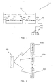
- FIG. 1 is a simplified timing diagram of such an exemplary bidirectional, half-duplex communication protocol 50 having temporally displaced receive 52 and transmit 54 time periods within each frame time 55.
- these relatively small receive 52 and transmit 54 time periods are separated by a relatively large intermessage delay time periods 56, 58.
- a master controller 60 (see FIG. 2 ) periodically sends command/status requests to one or more slaves 62a-62n (see FIG. 2 ) during receive period 52.
- Each slave 62 then transmits status/data information back to the master controller 60 during a transmit period 54 where the temporal position of transmit period 54 is defined at least in part by a unique identifier, e.g., a device ID, for each slave 62.
- a unique identifier e.g., a device ID
- the timing capability of each slave 62 must be sufficiently precise so that the transmit period 54 for each slave 62 will not overlap or otherwise interfere with another slave 62.
- the '991 patent teaches that power savings can be achieved by turning off portions of the communication circuitry when they are not needed, e.g., during the intermessage delay portions 56, 58. These power savings can be quite significant due to the relatively small percentage of the frame time 55 that receive and transmit circuitry portions are needed (see time periods 52, 54) versus the intermessage delay portions (see time periods 56, 58).
- a crystal oscillator is needed and since timing related to the crystal oscillator is used for determining the position of each time period, it must be operational throughout each cycle of the communication protocol 50. Accordingly, it is preferred that the selected crystal oscillator circuit consume relatively small amounts of power. Furthermore, it is preferred that the selected crystal oscillator circuit operate at a low voltage, e.g., preferably below 2 volts (0.9 volts in a preferred implementation). Such a crystal oscillator is described by Eric A. Vittoz, Marc G. R.
- Such a crystal oscillator (referred to herein as a Vittoz-type oscillator) reduces power by starving out the current needs of its FET circuitry to just above its critical needs during oscillation while providing an initial current startup burst to begin its oscillation.
- Embodiments of the present invention further reduce the power consumption of the selected oscillator, e.g., a Vittoz-type oscillator, by using a switching mode type of power supply to downconvert a power source to the operating voltage for the oscillator. Additionally, since such a switching mode power supply typically generates noise that could adversely effect communication capabilities, embodiments of the present invention switch to using a series downconverter mode power supply during the transmit 54 and/or receive 52 time periods.
- a switching mode type of power supply typically generates noise that could adversely effect communication capabilities
- FIG. 3 comprises a block diagram of an oscillator system 100 of the present invention wherein an oscillator 102, preferably a low power oscillator such as a Vittoz-type oscillator, is powered from at least two power supplies, a first one 104 that minimizes power consumption that is used during the intermessage delay portions 56, 58 and a second one 106 that minimizes noise generation that is used during the transmit 54 and/or receive 52 message portions.
- an oscillator 102 preferably a low power oscillator such as a Vittoz-type oscillator
- Oscillator 102 preferably runs off of a low voltage V o , e.g., 0.9 volts in a currently preferred implementation, and a low current, typically less than 50 ⁇ a and preferably less than 5 ⁇ a depending upon the programmed amplitude of oscillation to generate a frequency output f out , e.g., 25 MHz, suitable for division to obtain timing and modulation frequencies.
- V o low voltage
- a low current typically less than 50 ⁇ a and preferably less than 5 ⁇ a depending upon the programmed amplitude of oscillation to generate a frequency output f out , e.g., 25 MHz, suitable for division to obtain timing and modulation frequencies.
- Series downconverter mode power supply 106 operates in a conventional manner, e.g., in a constant voltage or current mode, to reduce the voltage V IN , e.g., 1.8 volts in a currently preferred implementation, to V o while switching downconverter mode power supply 104 operates on voltage V' IN , e.g., 2.7 volts in a currently preferred implementation, to reduce It to V o .
- Communication controller 108 operates upon communication signal 110 to retrieve status requests and control data and generates responsive signals 112.
- the communication controller 108 determines that it is processing the intermessage delay portions 56, 58, it activates the enable switching control line 114 to turn on the switching downconverter 104. Conversely, the enable series control line 116 is activated to turn on the series downconverter 106 during the receive 52 and/or transmit 54 time periods.
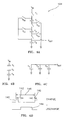
- FIG. 4A shows a simplified example of switching downconverter 104, suitable for use with the system 100 of FIG. 3 , which comprises a plurality of capacitors (C 1 -C 3 ) and switches (S 1 -S 3 , S 10 -S 13 ) for reconfiguring the charge and discharge paths to and from the capacitors to thus form a power efficient downconverter. While such a downconverter 104 is relatively power efficient as compared to the series downconverter 106, switching downconverter 104 does generate more noise (which is not desirable during receive 52 and/or transmit 54 time periods).
- an average current drain will be: time periods 56 + 58 / time periods 52 + 54 + 56 + 58 * 2.5 + time periods 52 + 54 / time periods 52 + 54 + 54 + 58 * peak current drain
- FIG. 4D a charging time period 140, capacitors C 1 , C 2 , C 3 are charged in series such that each one is charged to a voltage of one third of V IN .
- S 1 , S 2 , and S 3 are enabled while all of the other switches are disabled.
- FIG. 4B shows the configuration of the capacitors of FIG. 4A when the capacitors are being charged.
- all switches are disabled during a first inter-switching delay period 142 and then during a second time period, a discharging time period 144, switches S 1 -S 3 are disabled and the remaining switches S 10 -S 13 are enabled in order to supply a voltage of one third of V IN to V OUT .
- FIG. 4C shows the configuration of the capacitors of FIG. 4A when the capacitors are being discharged.
- all switches are again disabled during a second inter-switching delay period 146 and then the voltage downconversion cycle 148 recommences.
- the timing of the voltage downconversion cycle 148 is controlled according to a frequency division (not shown) of the crystal oscillator frequency f out .
- the oscillator system 100 of the present invention uses the series downconverter 106 to power the oscillator 102 during startup.
- FIGS. 7-10 are detailed schematics of a presently preferred implementation of the crystal oscillator system 100 (see FIG. 3 ) of the present invention (minus the programmable capacitance of FIGS. 11A , 11B ,12-14 ).
- FIG. 7 is the overall block diagram of the crystal oscillator system 100 including the crystal oscillator 102 and linear downconverter, i.e., series downconverter 106. Additionally, an output buffer 160 and power sequencing control logic 162 (this function has previously been considered to be a portion of communication controller 108) are additionally shown but the switching downconverter portion 104 of the system is shown in detail in FIG. 10 .
- FIG. 8 shows a detailed schematic of the crystal oscillator 102
- FIG. 9 shows a detailed schematic of the sequencing control logic 162.
- the crystal oscillator system 100 additionally includes circuitry for adjusting the frequency of the crystal oscillator 102.
- the crystal oscillator is essentially comprised of an inverting transconductance amplifier 164 (see FIG. 3 ) having its current source output connected to a second node 122 of the crystal 124 and a first node 120 of the crystal 124 connected'to the input of the inverting transconductance amplifier 164. Additionally, capacitors C p1 , C p2 are respectively coupled to connection nodes 120, 122.
- the crystal 124 has a series resonance frequency which is preferably selected to be slightly below a target frequency (approximately 25 MHz in a preferred implementation).
- oscillator 102 is configured to operate in a parallel resonance mode in which the crystal 124 oscillates at a frequency above (approximately 0.1 % above) the series resonance frequency.
- the operating frequency of an oscillator operated in a parallel resonance mode is determined by the amount of capacitive loading on the crystal.
- the highest frequency is initially determined by the parasitic capacitive (C p1 , C p2 ) loading on each of the connection nodes 120, 122 of the crystal 124.
- the capacitance increases (within limits) on either one of the operating nodes (120 or 122)
- the operating frequency decreases (nonlinearly) toward the series resonance frequency.
- the operating frequency of the oscillator 102 may be adjusted by coupling a programmable capacitance to either one of the crystal 124 connection nodes, i.e., node 120 or node 122.
- the programmable capacitance is formed from a plurality of capacitors C 1 -C N which are selectively combined with a plurality of switches 126, 128, preferably semiconductor switches such as FETs.
- the selection of which portions of switches 126, 128 are enabled is preferably determined by the output of a latch 130 under control of the communication controller 108 via a data bus 132 and a load clock 134.
- thermometer encoding due to the correspondence of the sequencing of at least a portion of its enable lines 136 1 -136 N to a conventional thermometer, ensures monoticity. This monoticity simplifies the closed loop control (described later) for controlling the frequency of the crystal oscillator 102.
- a coarse adjustment 128 (which uses the aforementioned thermometer decoder) is coupled with a fine adjustment 126 to achieve a sufficient range and precision of adjustment.
- Capacitors C 1 -C M and C M+1 -C N are selectively combined accordingly using their associated switches 128, 126 to achieve the coarse and fine adjustments.
- FIGS. 11A , 11B , 12-14 are detailed schematics of a presently-preferred implementation of the programmable capacitance 118 of FIG. 3 .
- a 12-bit value is used to select the capacitance value with the lower 4 bits, i.e., D0-D3, selecting one of sixteen capacitors ranging from 0.016 pf (picofarads) to 0.031 pf (forming the fine adjustment 126) and the upper 8 bits, i.e., D4-D11, selecting (using a plurality of thermometer decoders) from 1 to 256 capacitors (for forming the coarse adjustment 128), each of which having a value of 0.016 pf.
- FIG. 11A shows a plurality of thermometer decoders and associated trim capacitors which comprise an implementation of the coarse switches 128, FIG. 11B shows an implementation of the fine switches 126 and associated capacitors, FIG.12 shows a simplified schematic of a representative thermometer decoder, FIG. 13 shows a detailed schematic of a representative thermometer decoder, and FIG. 14 shows a detailed schematic of a representative trim capacitor and switch as used in FIG. 12 .
- the placement of the transmit portion 54 following the receive portion 52 is determined at least in part by a unique device ID.
- the relative placement of the transmit portion 54 is particularly significant in the exemplary protocol 50, i.e., intermessage delay 56 must be sufficiently precise to ensure a lack of interference between transmit portions 54 of the other slaves 62.
- the use of a phase locked loop in the slave device 62 is described which adjusts the phase of its clock to data received from the master device 60 in receive time period 52.
- a divide-by-N 170 is shown which divides f out to obtain a baud rate clock 172.
- the baud rate clock 172 is further divided by a divide-by-M 174 (where M is the product of the bauds per word and the number of words per frame) to obtain a frame rate clock 176.
- M is the product of the bauds per word and the number of words per frame
- the location of divide-bys 170 and 174 are only exemplary and they may be located elsewhere, e.g., in portions of the oscillator 102, communication controller 108, etc.
- embodiments of the present invention count M*N clocks of the oscillator frequency f out and then look for the phase of the baud rate clock of the received data on communication signal 110.
- phase error detector 178 which determines the correlation between the baud rate clock 172 and the received clock extracted from the communication signal 110
- this error signal 150 can be used as an indication of the direction and magnitude of the error in the frequency of oscillator 102.
- the oscillator frequency will be sufficiently precise that only a phase error will result.
- a unique portion of the received data e.g., a synchronization pattern, may be used as a time reference for generating the error signal.
- FIG. 6 shows a simplified block diagram of such a closed loop control system.
- the error signal 150 is measured. If the error signal 150 is zero (or within a designated range of zero) (see block 202), no adjustment is needed.
- the programmable capacitance 118 is decreased in block 206 to increase oscillator frequency.
- the programmable capacitance 118 is increased in block 208 to decrease the oscillator frequency.
- any adjustment is done according to the smallest possible step, e.g., a fine step of switch 126, so that the oscillator frequency adjusts smoothly toward the desired frequency without overshoot.
- the needed capacitance change may be calculated according to the measured error signal 150 to achieve the desired oscillator frequency in fewer iterations, i.e., faster (see the alternative path of block 210).
- Vittoz-type oscillator is the preferred oscillator type
- the present invention can beneficially improve the performance, i.e., decrease power consumption and decrease noise generation, of other oscillator structures as well.
- adjustable capacitance While a single adjustable capacitance has been shown coupled to either one of the connection nodes of the crystal, it is recognized that two adjustable capacitors may also be used where a first adjustable capacitance 118 is connected to the first node 120 and a second adjustable capacitor 118b (not shown but constructed in a similar manner to programmable capacitance 118) is connected to the second node 122. It is therefore to be understood that within the scope of the claims, the invention may be practiced otherwise than as specifically described herein.
Landscapes
- Oscillators With Electromechanical Resonators (AREA)
- Transceivers (AREA)
- Inductance-Capacitance Distribution Constants And Capacitance-Resistance Oscillators (AREA)
Claims (24)
- Kristalloszillatorsystem (100), das Folgendes umfasst:einen Kristalloszillator (102);eine erste Spannungsversorgung (104);eine zweite Spannungsversorgung (106);dadurch gekennzeichnet, dass das System aufgebaut ist, um entweder Stromverbrauch oder Rauscherzeugung zu minimieren, und Folgendes umfasst:eine Betriebsartenwechselschaltung (108), um den Kristalloszillator gemäß gewünschter Systemparameter entweder durch die erste oder durch die zweite Spannungsversorgung versorgen zu lassen, undworin die erste Spannungsversorgung den Kristalloszillator (102) in einer ersten Betriebsart mit Spannung versorgt und als Schaltabwärtswandler (104) arbeitet, um den Stromverbrauch zu minimieren, undworin die zweite Spannungsversorgung den Kristalloszillator in einer zweiten Betriebsart mit Spannung versorgt und als serieller Abwärtswandler (106) arbeitet, um die Rauscherzeugung zu minimieren.
- Kristalloszillatorsystem (100) nach Anspruch 1, das zur Verwendung in einem Kommunikationssystem aufgebaut ist, das gemäß einem Kommunikationsprotokoll arbeitet, wobei das Kommunikationsprotokoll so aufgebaut ist, dass der Großteil der Zeit für Verzögerungsabschnitte zwischen Nachrichten, und zwar zwischen Nachrichtenversende- und/oder Nachrichtenempfangsabschnitten, bestimmt ist, und wobei die Betriebsartenwechselschaltung die zweite Betriebsart während der Nachrichtenversende- und/oder -empfangsabschnitte wählt und die erste Betriebsart während der Verzögerungsabschnitte zwischen den Nachrichten wählt.
- Kristalloszillatorsystem (100) nach Anspruch 1 oder 2, das zur Verwendung in einem Kommunikationssystem einer implantierbaren Vorrichtung aufgebaut ist.
- Kristalloszillatorsystem (100) nach Anspruch 1, das zusätzlich eine Schaltung (118) zur Einstellung der Frequenz des Kristalloszillators (102) umfasst.
- Kristalloszillatorsystem (100) nach Anspruch 4, wobei der Kristalloszillator (102) einen Kristall (124) mit ersten und zweiten Verbindungsknoten umfasst und wobei die Frequenzeinstellungsschaltung (118) eine programmierbare Kapazität (118) umfasst, die zu einem ausgewählten Verbindungsknoten des Kristalls hinzugefügt wird, wodurch die Frequenz des Kristalloszillators (102) eingestellt wird.
- Kristalloszillatorsystem (100) nach Anspruch 5, worin die programmierbare Kapazität (118) eine Vielzahl an Kondensatoren umfasst, die programmierbar an den ausgewählten Verbindungsknoten angeschlossen sind.
- Kristalloszillator (102) nach Anspruch 6, worin die programmierbare Kapazität (118) eine grobeinstellbare Kapazität (128) zur Einstellung eines Einstellungsbereichs und eine feineinstellbare Kapazität (126) zur Einstellung der Kapazität in Bezug auf den Einstellungsbereich umfasst.
- Kristalloszillator (102) nach Anspruch 7, der zusätzlich einen Thermometer-Decoder umfasst, um die grobeinstellbare Kapazität zu bilden.
- Kristalloszillator (102) nach Anspruch 5, der zusätzlich eine Messschaltung zur Messung eines Frequenzfehlersignals umfasst, wobei die programmierbare Kapazität in Reaktion auf das Fehlersignal eingestellt wird, damit das Frequenzfehlersignal reduziert wird.
- Kristalloszillator (102) nach Anspruch 9, worin die Messschaltung das Frequenzfehlersignal periodisch misst.
- Kristalloszillator (102) nach Anspruch 9, worin die Messschaltung das Frequenzfehlersignal periodisch misst, indem ein Baud-Taktfehler in Bezug auf eine externe Referenz ermittelt wird.
- Kristalloszillator (102) nach Anspruch 9, worin die Messschaltung das Frequenzfehlersignal periodisch misst, indem ein Baud-Taktfehler in Bezug auf eine fixe Referenz in einem durch eine externe Quelle gesteuerten Kommunikationsprotokoll bestimmt.
- Kristalloszillator (102) nach Anspruch 9, worin die Messschaltung das Frequenzfehlersignal periodisch misst, indem ein Baud-Taktperiodenfehler in Bezug auf eine fixe Referenz in einem durch eine externe Quelle gesteuerten Kommunikationsprotokoll bestimmt.
- Kristalloszillator (102) nach Anspruch 10, worin die programmierbare Kapazität (118) eingestellt wird, um das Frequenzfehlersignal für die Dauer einer Reihe von Messungen zu minimieren.
- Kristalloszillatorsystem (100) nach Anspruch 4, worin der Kristalloszillator (100) einen Kristall (124) mit einer Reihenresonanzfrequenz, die unter einer Zielfrequenz liegt, umfasst und der Kristalloszillator (102) konfiguriert ist, um in einer Frequenz, die über der Reihenresonanzfrequenz liegt, in einer Parallelresonanzbetriebsart betrieben zu werden, und die Schaltung zur Einstellung der Frequenz des Kristalloszillators (102) bewirkt, dass die Frequenz des Oszillators programmierbar auf die Zielfrequenz eingestellt wird.
- Kristalloszillatorsystem (100) nach Anspruch 1, worin die erste Spannungsversorgung (104) als konstante Spannungsquelle arbeitet.
- Kristalloszillatorsystem (100) nach Anspruch 1, worin die erste Spannungsversorgung (104) als konstante Spannungsquelle arbeitet.
- Kristalloszillatorsystem (100) nach Anspruch 1, worin die zweite Spannungsversorgung (106) Folgendes umfasst:eine Vielzahl an Kondensatoren (C1, C2, C3) undeine Wechselschaltung (104), um die Kondensatoren entweder in Serie zu verbinden, damit diese kollektiv durch eine erste Spannung geladen werden, oder parallel zu verbinden, um kollektiv eine Ladung durch eine zweite Spannung bereitzustellen, die geringer als die erste Spannung ist.
- Kristalloszillatorsystem (100) nach Anspruch 18, worin die zweite Spannung im Wesentlichen ein ganzzahliger Bruchteil der ersten Spannung ist.
- Kristalloszillatorsystem nach Anspruch 19, worin die zweite Spannungsversorgung drei Kondensatoren (C1, C2, C3) umfasst und die zweite Spannung im Wesentlichen ein Drittel der ersten Spannung beträgt.
- Verfahren, um entweder den Stromverbrauch oder die Rauscherzeugung eines Kristalloszillators (102) zu minimieren, das geeignet ist, um in einem Kommunikationssystem angewandt zu werden, das gemäß einem Kommunikationsprotokoll arbeitet, wobei das Kommunikationsprotokoll so aufgebaut ist, dass der Großteil der Zeit für Verzögerungsabschnitte zwischen Nachrichten, und zwar zwischen Nachrichtenversende- und/oder Nachrichtenempfangsabschnitten, bestimmt ist, wobei das Verfahren folgende Schritte umfasst:die Spannungsversorgung des Kristalloszillators (102) über eine Spannungsversorgung in Form eines seriellen Abwärtswandlers (106) während der Nachrichtenversende- und/oder Nachrichtenempfangsabschnitte; unddie Spannungsversorgung des Kristalloszillators (102) über eine Schaltstromversorgung (104) während der Verzögerungsabschnitte zwischen Nachrichten.
- Verfahren nach Anspruch 21, worin der Schritt der Spannungsversorgung des Kristalloszillators (102) über eine Spannungsversorgung in Form eines seriellen Abwärtswandlers (106) das Aufrechterhalten eines konstanten Stromausgangssignals umfasst.
- Verfahren nach Anspruch 21, worin der Schritt der Spannungsversorgung des Kristalloszillators (102) über eine Schaltabwärtswandlerspannungsversorgung das Aufrechterhalten eines konstanten Spannungsausgangssignals umfasst.
- Verfahren nach Anspruch 21, worin der Schritt der Spannungsversorgung des Kristalloszillators (102) über eine Schaltabwärtswandlerspannungsversorgung folgende Schritte umfasst:das periodische Laden einer Vielzahl an Kondensatoren (C1, C2, C3), die in Serie geschaltet sind, durch eine Spannungsquelle bei einem ersten Spannungspegel unddas periodische Laden einer Vielzahl an Kondensatoren (C1, C2, C3), die parallel geschaltet sind, bei einem zweiten Spannungspegel, wobei der zweite Spannungspegel im Wesentlichen ein ganzzahliger Bruchteil des ersten Spannungspegels ist.
Applications Claiming Priority (3)
| Application Number | Priority Date | Filing Date | Title |
|---|---|---|---|
| US10/280,841 US6959217B2 (en) | 2002-10-24 | 2002-10-24 | Multi-mode crystal oscillator system selectively configurable to minimize power consumption or noise generation |
| US280841 | 2002-10-24 | ||
| PCT/US2003/031634 WO2004038908A2 (en) | 2002-10-24 | 2003-10-06 | Multi-mode crystal oscillator system selectively configurable to minimize power consumption or noise generation |
Publications (3)
| Publication Number | Publication Date |
|---|---|
| EP1554010A2 EP1554010A2 (de) | 2005-07-20 |
| EP1554010A4 EP1554010A4 (de) | 2011-03-23 |
| EP1554010B1 true EP1554010B1 (de) | 2012-12-05 |
Family
ID=32107033
Family Applications (1)
| Application Number | Title | Priority Date | Filing Date |
|---|---|---|---|
| EP03773172A Expired - Lifetime EP1554010B1 (de) | 2002-10-24 | 2003-10-06 | Selektiv konfigurierbares multimodus-kristalloszillator-system zur minimierung des stromverbrauchs oder der geräuscherzeugung |
Country Status (4)
| Country | Link |
|---|---|
| US (1) | US6959217B2 (de) |
| EP (1) | EP1554010B1 (de) |
| AU (1) | AU2003279844A1 (de) |
| WO (1) | WO2004038908A2 (de) |
Families Citing this family (89)
| Publication number | Priority date | Publication date | Assignee | Title |
|---|---|---|---|---|
| US7406105B2 (en) | 2004-03-03 | 2008-07-29 | Alfred E. Mann Foundation For Scientific Research | System and method for sharing a common communication channel between multiple systems of implantable medical devices |
| US7266349B2 (en) * | 2004-08-06 | 2007-09-04 | Broadcom Corporation | Multi-mode crystal oscillator |
| US7536164B2 (en) * | 2004-09-30 | 2009-05-19 | Silicon Laboratories Inc. | Controlling the frequency of an oscillator |
| US7689190B2 (en) * | 2004-09-30 | 2010-03-30 | St-Ericsson Sa | Controlling the frequency of an oscillator |
| KR100839486B1 (ko) * | 2005-03-07 | 2008-06-19 | 삼성전자주식회사 | 듀얼 모드 튜닝 디지털 제어 크리스탈 발진기 및 그 동작방법 |
| US7370214B2 (en) * | 2005-03-24 | 2008-05-06 | Silicon Laboratories Inc. | Automatically switching power supply sources for a clock circuit |
| US8802183B2 (en) | 2005-04-28 | 2014-08-12 | Proteus Digital Health, Inc. | Communication system with enhanced partial power source and method of manufacturing same |
| US8912908B2 (en) | 2005-04-28 | 2014-12-16 | Proteus Digital Health, Inc. | Communication system with remote activation |
| US8730031B2 (en) | 2005-04-28 | 2014-05-20 | Proteus Digital Health, Inc. | Communication system using an implantable device |
| US9198608B2 (en) | 2005-04-28 | 2015-12-01 | Proteus Digital Health, Inc. | Communication system incorporated in a container |
| JP2008539047A (ja) | 2005-04-28 | 2008-11-13 | プロテウス バイオメディカル インコーポレイテッド | ファーマインフォーマティックスシステム |
| US8836513B2 (en) | 2006-04-28 | 2014-09-16 | Proteus Digital Health, Inc. | Communication system incorporated in an ingestible product |
| US20070004362A1 (en) * | 2005-06-30 | 2007-01-04 | Lawrence Der | Methods and apparatus to generate small frequency changes |
| US7587184B2 (en) * | 2005-06-30 | 2009-09-08 | Silicon Laboratories Inc. | Controlling fine frequency changes in an oscillator |
| US8547248B2 (en) * | 2005-09-01 | 2013-10-01 | Proteus Digital Health, Inc. | Implantable zero-wire communications system |
| US8160704B2 (en) * | 2005-11-02 | 2012-04-17 | Cardiac Pacemakers, Inc. | System and method for enabling relayed communications by implantable medical devices |
| US7668600B2 (en) * | 2006-01-19 | 2010-02-23 | Medtronic, Inc. | System and method for telemetry with an implantable medical device |
| US7414482B2 (en) * | 2006-02-10 | 2008-08-19 | Broadcom Corporation | Resonance mode selection using a resonator-synchronized second-order oscillator |
| US7741920B2 (en) * | 2006-02-10 | 2010-06-22 | Broadcom Corporation | Quadrature oscillator with simplified amplitude, phase and frequency control |
| US7902933B1 (en) * | 2006-03-29 | 2011-03-08 | Cypress Semiconductor Corporation | Oscillator circuit |
| EP2013829A4 (de) | 2006-05-02 | 2010-07-07 | Proteus Biomedical Inc | Patientenspezifische therapieformen |
| US20080132178A1 (en) * | 2006-09-22 | 2008-06-05 | Shouri Chatterjee | Performing automatic frequency control |
| WO2008066617A2 (en) * | 2006-10-17 | 2008-06-05 | Proteus Biomedical, Inc. | Low voltage oscillator for medical devices |
| US8945005B2 (en) | 2006-10-25 | 2015-02-03 | Proteus Digital Health, Inc. | Controlled activation ingestible identifier |
| EP2069004A4 (de) | 2006-11-20 | 2014-07-09 | Proteus Digital Health Inc | Persönliche gesundheitssignalempfänger mit aktiver signalverarbeitung |
| KR101475666B1 (ko) | 2007-02-01 | 2014-12-23 | 프로테우스 디지털 헬스, 인코포레이티드 | 섭취 가능한 이벤트 마커 시스템 |
| JP5614991B2 (ja) | 2007-02-14 | 2014-10-29 | プロテウス デジタル ヘルス, インコーポレイテッド | 大表面積電極を有する体内型電源 |
| US8932221B2 (en) | 2007-03-09 | 2015-01-13 | Proteus Digital Health, Inc. | In-body device having a multi-directional transmitter |
| WO2008112578A1 (en) | 2007-03-09 | 2008-09-18 | Proteus Biomedical, Inc. | In-body device having a deployable antenna |
| US8540632B2 (en) | 2007-05-24 | 2013-09-24 | Proteus Digital Health, Inc. | Low profile antenna for in body device |
| ES2928197T3 (es) | 2007-09-25 | 2022-11-16 | Otsuka Pharma Co Ltd | Dispositivo intracorpóreo con amplificación de señal de dipolo virtual |
| US20090085684A1 (en) * | 2007-10-01 | 2009-04-02 | Silicon Laboratories Inc. | Low power rtc oscillator |
| CA2717809A1 (en) | 2007-11-27 | 2009-06-04 | Proteus Biomedical, Inc. | Transbody communication systems employing communication channels |
| DK2268261T3 (en) | 2008-03-05 | 2017-08-28 | Proteus Digital Health Inc | Edible event markers with multi-mode communications and systems as well as methods for using them |
| MY154234A (en) | 2008-07-08 | 2015-05-15 | Proteus Digital Health Inc | Ingestible event marker data framework |
| CA2734251A1 (en) | 2008-08-13 | 2010-02-18 | Proteus Biomedical, Inc. | Ingestible circuitry |
| CN102245259B (zh) * | 2008-11-13 | 2013-06-12 | 普罗秋斯数字健康公司 | 可摄入的治疗激活器系统及方法 |
| CA2746650A1 (en) * | 2008-12-11 | 2010-06-17 | Proteus Biomedical, Inc. | Evaluation of gastrointestinal function using portable electroviscerography systems and methods of using the same |
| TWI424832B (zh) | 2008-12-15 | 2014-02-01 | Proteus Digital Health Inc | 與身體有關的接收器及其方法 |
| US9439566B2 (en) | 2008-12-15 | 2016-09-13 | Proteus Digital Health, Inc. | Re-wearable wireless device |
| US9659423B2 (en) | 2008-12-15 | 2017-05-23 | Proteus Digital Health, Inc. | Personal authentication apparatus system and method |
| EP2385781A4 (de) | 2009-01-06 | 2014-11-05 | Proteus Digital Health Inc | Nahrungsaufnahme-biofeedback sowie personalisiertes medizinisches therapieverfahren und -system |
| TWI544917B (zh) | 2009-01-06 | 2016-08-11 | 波提亞斯數位康健公司 | 醫藥劑量傳送系統 |
| US9370664B2 (en) | 2009-01-15 | 2016-06-21 | Boston Scientific Neuromodulation Corporation | Signaling error conditions in an implantable medical device system using simple charging coil telemetry |
| GB2480965B (en) | 2009-03-25 | 2014-10-08 | Proteus Digital Health Inc | Probablistic pharmacokinetic and pharmacodynamic modeling |
| EP2246094B1 (de) * | 2009-04-28 | 2011-03-09 | Sorin CRM SAS | Induktives Schaltnetzteil mit digitaler Steuerung für aktive implantierbare medizinische Vorrichtung |
| NZ619375A (en) | 2009-04-28 | 2015-03-27 | Proteus Digital Health Inc | Highly reliable ingestible event markers and methods for using the same |
| US9149423B2 (en) | 2009-05-12 | 2015-10-06 | Proteus Digital Health, Inc. | Ingestible event markers comprising an ingestible component |
| WO2011022732A2 (en) | 2009-08-21 | 2011-02-24 | Proteus Biomedical, Inc. | Apparatus and method for measuring biochemical parameters |
| TWI517050B (zh) | 2009-11-04 | 2016-01-11 | 普羅托斯數位健康公司 | 供應鏈管理之系統 |
| UA109424C2 (uk) | 2009-12-02 | 2015-08-25 | Фармацевтичний продукт, фармацевтична таблетка з електронним маркером і спосіб виготовлення фармацевтичної таблетки | |
| RU2587795C2 (ru) | 2010-02-01 | 2016-06-20 | Проутьюс Диджитал Хэлс, Инк. | Система сбора данных |
| US8266750B2 (en) | 2010-03-24 | 2012-09-18 | Gatelink Aircraft Boarding Systems, Inc. | Microbridges for regional aircraft and methods of using same |
| US9597487B2 (en) | 2010-04-07 | 2017-03-21 | Proteus Digital Health, Inc. | Miniature ingestible device |
| TWI557672B (zh) | 2010-05-19 | 2016-11-11 | 波提亞斯數位康健公司 | 用於從製造商跟蹤藥物直到患者之電腦系統及電腦實施之方法、用於確認將藥物給予患者的設備及方法、患者介面裝置 |
| US20120035557A1 (en) * | 2010-07-16 | 2012-02-09 | Timothy Woodrow Coffindaffer | Personal Care Compositions Comprising A Multi-Active System For Down Regulating Cytokines Irritation |
| US9107806B2 (en) | 2010-11-22 | 2015-08-18 | Proteus Digital Health, Inc. | Ingestible device with pharmaceutical product |
| US8766788B2 (en) | 2010-12-20 | 2014-07-01 | Abiomed, Inc. | Transcutaneous energy transfer system with vibration inducing warning circuitry |
| EP2654878B1 (de) | 2010-12-20 | 2019-05-15 | Abiomed, Inc. | Transkutanes energieübertragungssystem mit mehreren sekundären spulen |
| JP2014502528A (ja) | 2010-12-20 | 2014-02-03 | アビオメド インコーポレイティド | 経皮エネルギー伝送システムにおいて使用可能な充電を正確に追跡するための方法および装置 |
| EP2683291B1 (de) | 2011-03-11 | 2019-07-31 | Proteus Digital Health, Inc. | Am körper tragbare persönliche vorrichtung mit verschiedenen physikalischen konfigurationen |
| EP2697890B1 (de) | 2011-04-14 | 2019-02-20 | Abiomed, Inc. | Transkutane energieübertragungsspule mit integrierter funkfrequenzantenne |
| WO2015112603A1 (en) | 2014-01-21 | 2015-07-30 | Proteus Digital Health, Inc. | Masticable ingestible product and communication system therefor |
| US9756874B2 (en) | 2011-07-11 | 2017-09-12 | Proteus Digital Health, Inc. | Masticable ingestible product and communication system therefor |
| EP2734973A4 (de) | 2011-07-21 | 2015-07-01 | Proteus Digital Health Inc | Mobilkommunikationsvorrichtung, -system und -verfahren |
| US9235683B2 (en) | 2011-11-09 | 2016-01-12 | Proteus Digital Health, Inc. | Apparatus, system, and method for managing adherence to a regimen |
| US9002468B2 (en) | 2011-12-16 | 2015-04-07 | Abiomed, Inc. | Automatic power regulation for transcutaneous energy transfer charging system |
| BR112015001388A2 (pt) | 2012-07-23 | 2017-07-04 | Proteus Digital Health Inc | técnicas para fabricar marcadores de eventos ingeríveis que compreendem um componente ingerível |
| WO2014062674A1 (en) | 2012-10-18 | 2014-04-24 | Proteus Digital Health, Inc. | Apparatus, system, and method to adaptively optimize power dissipation and broadcast power in a power source for a communication device |
| WO2014120669A1 (en) | 2013-01-29 | 2014-08-07 | Proteus Digital Health, Inc. | Highly-swellable polymeric films and compositions comprising the same |
| WO2014151929A1 (en) | 2013-03-15 | 2014-09-25 | Proteus Digital Health, Inc. | Personal authentication apparatus system and method |
| JP5941240B2 (ja) | 2013-03-15 | 2016-06-29 | プロテウス デジタル ヘルス, インコーポレイテッド | 金属検出器装置、システム、および方法 |
| EP3005281A4 (de) | 2013-06-04 | 2017-06-28 | Proteus Digital Health, Inc. | System, vorrichtung und verfahren zur datensammlung und ergebnisbeurteilung |
| US9796576B2 (en) | 2013-08-30 | 2017-10-24 | Proteus Digital Health, Inc. | Container with electronically controlled interlock |
| EP3047618B1 (de) | 2013-09-20 | 2023-11-08 | Otsuka Pharmaceutical Co., Ltd. | Verfahren, vorrichtungen und systeme zum empfang und zur decodierung eines signals in der gegenwart von rauschen mit slices und verzerrung |
| WO2015044722A1 (en) | 2013-09-24 | 2015-04-02 | Proteus Digital Health, Inc. | Method and apparatus for use with received electromagnetic signal at a frequency not known exactly in advance |
| US10084880B2 (en) | 2013-11-04 | 2018-09-25 | Proteus Digital Health, Inc. | Social media networking based on physiologic information |
| US11051543B2 (en) | 2015-07-21 | 2021-07-06 | Otsuka Pharmaceutical Co. Ltd. | Alginate on adhesive bilayer laminate film |
| KR102215238B1 (ko) | 2016-07-22 | 2021-02-22 | 프로테우스 디지털 헬스, 인코포레이티드 | 섭취 가능한 이벤트 마커의 전자기 감지 및 검출 |
| KR102605670B1 (ko) | 2016-10-26 | 2023-11-24 | 오츠카 세이야쿠 가부시키가이샤 | 섭취 가능한 이벤트 마커를 갖는 캡슐을 제조하는 방법 |
| US11128742B2 (en) | 2019-03-08 | 2021-09-21 | Microsemi Storage Solutions, Inc. | Method for adapting a constant bit rate client signal into the path layer of a telecom signal |
| WO2021223970A1 (en) * | 2020-05-06 | 2021-11-11 | Biotronik Se & Co. Kg | Local supply voltage regulation of a rechargeable medical implant via resonance tuning |
| US12323334B2 (en) | 2021-06-30 | 2025-06-03 | Microchip Technology Inc. | System and method for performing rate adaptation and multiplexing of constant bit rate (CBR) client data for transmission over a metro transport network (MTN) |
| US11916662B2 (en) | 2021-06-30 | 2024-02-27 | Microchip Technology Inc. | System and method for performing rate adaptation of constant bit rate (CBR) client data with a fixed number of idle blocks for transmission over a metro transport network (MTN) |
| US11838111B2 (en) | 2021-06-30 | 2023-12-05 | Microchip Technology Inc. | System and method for performing rate adaptation of constant bit rate (CBR) client data with a variable number of idle blocks for transmission over a metro transport network (MTN) |
| US11736065B2 (en) | 2021-10-07 | 2023-08-22 | Microchip Technology Inc. | Method and apparatus for conveying clock-related information from a timing device |
| US12192079B2 (en) | 2021-11-23 | 2025-01-07 | Microchip Technology Inc. | Method and apparatus for carrying constant bit rate (CBR) client signals using CBR carrier streams comprising frames |
| US11799626B2 (en) | 2021-11-23 | 2023-10-24 | Microchip Technology Inc. | Method and apparatus for carrying constant bit rate (CBR) client signals |
| US12500822B2 (en) | 2022-04-04 | 2025-12-16 | Microchip Technology Inc. | System and method for rate adaptation of packet-oriented client data for transmission over a metro transport network (MTN) |
Family Cites Families (18)
| Publication number | Priority date | Publication date | Assignee | Title |
|---|---|---|---|---|
| JPS59168704A (ja) * | 1983-03-14 | 1984-09-22 | Nec Corp | 半導体集積回路 |
| JPS61195388A (ja) * | 1985-02-26 | 1986-08-29 | Mitsubishi Electric Corp | 時計装置 |
| US5569307A (en) | 1989-09-22 | 1996-10-29 | Alfred E. Mann Foundation For Scientific Research | Implantable cochlear stimulator having backtelemetry handshake signal |
| US5531774A (en) | 1989-09-22 | 1996-07-02 | Alfred E. Mann Foundation For Scientific Research | Multichannel implantable cochlear stimulator having programmable bipolar, monopolar or multipolar electrode configurations |
| US5522865A (en) | 1989-09-22 | 1996-06-04 | Alfred E. Mann Foundation For Scientific Research | Voltage/current control system for a human tissue stimulator |
| US5603726A (en) | 1989-09-22 | 1997-02-18 | Alfred E. Mann Foundation For Scientific Research | Multichannel cochlear implant system including wearable speech processor |
| US5938691A (en) | 1989-09-22 | 1999-08-17 | Alfred E. Mann Foundation | Multichannel implantable cochlear stimulator |
| US5876425A (en) | 1989-09-22 | 1999-03-02 | Advanced Bionics Corporation | Power control loop for implantable tissue stimulator |
| JP3019340B2 (ja) * | 1989-12-05 | 2000-03-13 | セイコーエプソン株式会社 | 可変容量装置 |
| US5369376A (en) * | 1991-11-29 | 1994-11-29 | Standard Microsystems, Inc. | Programmable phase locked loop circuit and method of programming same |
| DE69832713T2 (de) | 1997-02-26 | 2006-07-27 | Alfred E. Mann Foundation For Scientific Research, Santa Clarita | Batterie-betriebsgerät zur implantation in einem patienten |
| US6164284A (en) | 1997-02-26 | 2000-12-26 | Schulman; Joseph H. | System of implantable devices for monitoring and/or affecting body parameters |
| US6563390B1 (en) * | 2000-12-29 | 2003-05-13 | Cypress Semiconductor Corp. | Digitally compensated voltage controlled oscillator |
| KR100379610B1 (ko) * | 2001-04-18 | 2003-04-08 | 삼성전자주식회사 | 전압 레벨 차이로 인한 누설 전류를 효과적으로 차단할 수있는 전압 레벨 변환 장치를 구비한 온-칩 시스템 |
| US6472991B1 (en) * | 2001-06-15 | 2002-10-29 | Alfred E. Mann Foundation For Scientific Research | Multichannel communication protocol configured to extend the battery life of an implantable device |
| KR100429895B1 (ko) * | 2001-11-21 | 2004-05-03 | 한국전자통신연구원 | 복수개의 출력을 가지는 레벨 시프터 |
| GB2402273B (en) * | 2003-05-30 | 2006-03-01 | Qualcomm | An apparatus for providing an oscillating signal to a load |
| JP2008053784A (ja) * | 2006-08-22 | 2008-03-06 | Toshiba Corp | 電圧制御発振器、電圧制御発振器用のバイアス装置、電圧制御発振器のバイアス調整プログラム |
-
2002
- 2002-10-24 US US10/280,841 patent/US6959217B2/en not_active Expired - Lifetime
-
2003
- 2003-10-06 AU AU2003279844A patent/AU2003279844A1/en not_active Abandoned
- 2003-10-06 WO PCT/US2003/031634 patent/WO2004038908A2/en not_active Ceased
- 2003-10-06 EP EP03773172A patent/EP1554010B1/de not_active Expired - Lifetime
Also Published As
| Publication number | Publication date |
|---|---|
| US6959217B2 (en) | 2005-10-25 |
| EP1554010A4 (de) | 2011-03-23 |
| US20040082982A1 (en) | 2004-04-29 |
| AU2003279844A1 (en) | 2004-05-13 |
| AU2003279844A8 (en) | 2004-05-13 |
| WO2004038908A2 (en) | 2004-05-06 |
| EP1554010A2 (de) | 2005-07-20 |
| WO2004038908A3 (en) | 2005-03-10 |
Similar Documents
| Publication | Publication Date | Title |
|---|---|---|
| EP1554010B1 (de) | Selektiv konfigurierbares multimodus-kristalloszillator-system zur minimierung des stromverbrauchs oder der geräuscherzeugung | |
| US9998124B2 (en) | Low power clock source | |
| KR101849985B1 (ko) | 모바일 애플리케이션들에서 배터리 수명을 연장시키기 위한 전자 디바이스 | |
| US7321755B2 (en) | Dual-mode clock for improved power management in a wireless device | |
| US8188782B1 (en) | Clock system and method for compensating timing information of clock system | |
| EP0905877A1 (de) | Oszillatorschaltung, elektronische schaltung, halbleiterbauelement, elektronische anordnung und uhr | |
| WO1991001591A1 (en) | Multiple bandwidth crystal controlled oscillator | |
| WO2009040329A1 (en) | Single multi-mode clock source for wireless devices | |
| CN103296968A (zh) | 用于休眠模式无线电的低功率定时的系统和方法 | |
| AU759155B2 (en) | Oscillator using calibration means | |
| JPH09509037A (ja) | 低電力温度補償水晶発振器 | |
| WO2015179429A1 (en) | Crystal oscillator startup time reduction | |
| EP0939495A1 (de) | Batteriesparanordnung für ein tragbares Gerät | |
| US20110257706A1 (en) | Low energy communications for implanted medical devices | |
| US7616066B2 (en) | Oscillation device and controlling method therefor | |
| EP0503888B1 (de) | Vorspannungs-Erzeugungsschaltung für ECL-Pegel mit Verringerung des Leistungsverbrauchs derselben | |
| KR100691369B1 (ko) | 바디 바이어스 조절형 전압제어발진기 | |
| US20220046538A1 (en) | Timing precision maintenance with reduced power during system sleep | |
| CN113037215B (zh) | 一种晶振控制电路及电子设备 | |
| WO2021202871A1 (en) | Wireless sensor reader with software-controlled power exciter and method for operating the same | |
| EP1514343B1 (de) | Anordnung zur taktgeneration mit niedriger leistung | |
| JP2002305443A (ja) | タイマー回路 | |
| JP3787471B2 (ja) | 無線検針装置 | |
| US20220326346A1 (en) | Dynamic power management in low power radar solutions | |
| US12457459B2 (en) | Crystal oscillator power reduction mechanism |
Legal Events
| Date | Code | Title | Description |
|---|---|---|---|
| PUAI | Public reference made under article 153(3) epc to a published international application that has entered the european phase |
Free format text: ORIGINAL CODE: 0009012 |
|
| 17P | Request for examination filed |
Effective date: 20050421 |
|
| AK | Designated contracting states |
Kind code of ref document: A2 Designated state(s): AT BE BG CH CY CZ DE DK EE ES FI FR GB GR HU IE IT LI LU MC NL PT RO SE SI SK TR |
|
| AX | Request for extension of the european patent |
Extension state: AL LT LV MK |
|
| DAX | Request for extension of the european patent (deleted) | ||
| RBV | Designated contracting states (corrected) |
Designated state(s): DE GB |
|
| A4 | Supplementary search report drawn up and despatched |
Effective date: 20110218 |
|
| 17Q | First examination report despatched |
Effective date: 20110802 |
|
| GRAP | Despatch of communication of intention to grant a patent |
Free format text: ORIGINAL CODE: EPIDOSNIGR1 |
|
| RIC1 | Information provided on ipc code assigned before grant |
Ipc: H03L 7/08 20060101ALI20120605BHEP Ipc: H03L 7/00 20060101ALI20120605BHEP Ipc: A61N 1/08 20060101ALI20120605BHEP Ipc: A61N 1/00 20060101AFI20120605BHEP |
|
| GRAS | Grant fee paid |
Free format text: ORIGINAL CODE: EPIDOSNIGR3 |
|
| GRAA | (expected) grant |
Free format text: ORIGINAL CODE: 0009210 |
|
| AK | Designated contracting states |
Kind code of ref document: B1 Designated state(s): DE GB |
|
| REG | Reference to a national code |
Ref country code: GB Ref legal event code: FG4D |
|
| REG | Reference to a national code |
Ref country code: DE Ref legal event code: R096 Ref document number: 60342775 Country of ref document: DE Effective date: 20130131 |
|
| PLBE | No opposition filed within time limit |
Free format text: ORIGINAL CODE: 0009261 |
|
| STAA | Information on the status of an ep patent application or granted ep patent |
Free format text: STATUS: NO OPPOSITION FILED WITHIN TIME LIMIT |
|
| 26N | No opposition filed |
Effective date: 20130906 |
|
| REG | Reference to a national code |
Ref country code: DE Ref legal event code: R097 Ref document number: 60342775 Country of ref document: DE Effective date: 20130906 |
|
| PGFP | Annual fee paid to national office [announced via postgrant information from national office to epo] |
Ref country code: GB Payment date: 20221027 Year of fee payment: 20 Ref country code: DE Payment date: 20221027 Year of fee payment: 20 |
|
| REG | Reference to a national code |
Ref country code: DE Ref legal event code: R071 Ref document number: 60342775 Country of ref document: DE |
|
| REG | Reference to a national code |
Ref country code: GB Ref legal event code: PE20 Expiry date: 20231005 |
|
| PG25 | Lapsed in a contracting state [announced via postgrant information from national office to epo] |
Ref country code: GB Free format text: LAPSE BECAUSE OF EXPIRATION OF PROTECTION Effective date: 20231005 |
|
| PG25 | Lapsed in a contracting state [announced via postgrant information from national office to epo] |
Ref country code: GB Free format text: LAPSE BECAUSE OF EXPIRATION OF PROTECTION Effective date: 20231005 |