EP1553814A1 - Electromagnetic wave shield case and a method for manufacturing electromagnetic wave shield case - Google Patents
Electromagnetic wave shield case and a method for manufacturing electromagnetic wave shield case Download PDFInfo
- Publication number
- EP1553814A1 EP1553814A1 EP05000119A EP05000119A EP1553814A1 EP 1553814 A1 EP1553814 A1 EP 1553814A1 EP 05000119 A EP05000119 A EP 05000119A EP 05000119 A EP05000119 A EP 05000119A EP 1553814 A1 EP1553814 A1 EP 1553814A1
- Authority
- EP
- European Patent Office
- Prior art keywords
- shield case
- flange
- electromagnetic wave
- wave shield
- circuit board
- Prior art date
- Legal status (The legal status is an assumption and is not a legal conclusion. Google has not performed a legal analysis and makes no representation as to the accuracy of the status listed.)
- Granted
Links
Images


Classifications
-
- H—ELECTRICITY
- H05—ELECTRIC TECHNIQUES NOT OTHERWISE PROVIDED FOR
- H05K—PRINTED CIRCUITS; CASINGS OR CONSTRUCTIONAL DETAILS OF ELECTRIC APPARATUS; MANUFACTURE OF ASSEMBLAGES OF ELECTRICAL COMPONENTS
- H05K9/00—Screening of apparatus or components against electric or magnetic fields
-
- H—ELECTRICITY
- H05—ELECTRIC TECHNIQUES NOT OTHERWISE PROVIDED FOR
- H05K—PRINTED CIRCUITS; CASINGS OR CONSTRUCTIONAL DETAILS OF ELECTRIC APPARATUS; MANUFACTURE OF ASSEMBLAGES OF ELECTRICAL COMPONENTS
- H05K9/00—Screening of apparatus or components against electric or magnetic fields
- H05K9/0007—Casings
- H05K9/002—Casings with localised screening
- H05K9/0022—Casings with localised screening of components mounted on printed circuit boards [PCB]
- H05K9/0024—Shield cases mounted on a PCB, e.g. cans or caps or conformal shields
- H05K9/0026—Shield cases mounted on a PCB, e.g. cans or caps or conformal shields integrally formed from metal sheet
-
- H—ELECTRICITY
- H05—ELECTRIC TECHNIQUES NOT OTHERWISE PROVIDED FOR
- H05K—PRINTED CIRCUITS; CASINGS OR CONSTRUCTIONAL DETAILS OF ELECTRIC APPARATUS; MANUFACTURE OF ASSEMBLAGES OF ELECTRICAL COMPONENTS
- H05K9/00—Screening of apparatus or components against electric or magnetic fields
- H05K9/0069—Methods for measuring the shielding efficiency; Apparatus therefor; Isolation container for testing
-
- H—ELECTRICITY
- H01—ELECTRIC ELEMENTS
- H01F—MAGNETS; INDUCTANCES; TRANSFORMERS; SELECTION OF MATERIALS FOR THEIR MAGNETIC PROPERTIES
- H01F1/00—Magnets or magnetic bodies characterised by the magnetic materials therefor; Selection of materials for their magnetic properties
- H01F1/01—Magnets or magnetic bodies characterised by the magnetic materials therefor; Selection of materials for their magnetic properties of inorganic materials
- H01F1/03—Magnets or magnetic bodies characterised by the magnetic materials therefor; Selection of materials for their magnetic properties of inorganic materials characterised by their coercivity
- H01F1/12—Magnets or magnetic bodies characterised by the magnetic materials therefor; Selection of materials for their magnetic properties of inorganic materials characterised by their coercivity of soft-magnetic materials
- H01F1/14—Magnets or magnetic bodies characterised by the magnetic materials therefor; Selection of materials for their magnetic properties of inorganic materials characterised by their coercivity of soft-magnetic materials metals or alloys
- H01F1/147—Alloys characterised by their composition
- H01F1/153—Amorphous metallic alloys, e.g. glassy metals
- H01F1/15358—Making agglomerates therefrom, e.g. by pressing
Definitions
- the present invention relates to an electromagnetic wave shield case disposed to cover electronic parts on a circuit board (printed circuit board) used for a cellular phone and a computer, and an electromagnetic wave shield case manufacturing method.
- an electromagnetic wave shield case essentially made of metallic materials, which are of a conductive substance.
- shield case When such an electromagnetic wave shield case (hereinafter referred to as “shield case” when appropriate) is located on the circuit board, as shown in Fig.1, a metallic ground line 3 (portion conducted to the earth (“grounding conduction portion”, hereinafter)) is provided in a region on a circuit board 1 corresponding to the lowermost portion of a shield case 50A and around it.
- the metallic ground line 3, and the lowermost portion of the shield case 50A, or part of the lowermost portion thereof are joined by soldering, and a soldering joint portion 4 is formed.
- Prior Art #2 which was developed by the Inventors of this application, solves the problems (a) to (e), whereby a shield case, in which an anchor pin integrally united thereto without soldering and has bending elasticity, is elastically joined to a through hole provided in a circuit board (for example, Japanese Patent Application Laid-open No. 2003-179378).
- Prior Art #3 was also developed by the Inventors of this application to solve the problems (a) to (e).
- a lock pin having bending elasticity which is integrally united with a back surface of a shield case without soldering, is elastically jointed to a housing for a circuit board.
- Zr group amorphous alloy metallic glass having high amorphous forming ability as well as high strength and ductility, which has been developed by the Inventors of this application, has also been known (for example, Japanese Patent Application Laid-open Nos. 2000-129378 and 2000-178700).
- Prior Art #1 has a problem in that the height of the shield case 50B is apt to be high, and a reduction in the thickness of the circuit board 1 is disturbed, resulting in a high cost of manufacturing.
- Prior Art #3 does not require provision of a through hole in a circuit board, Prior Art #3 has the following new problem regarding realization of a reliable electric connection of the shield case and the metallic ground line.
- a grounding interval for the shield case and the metallic ground line is required to be shorter.
- the shield case In order to manufacture the shield case, in a conventional method in which a crystalline metallic material is formed by bending or deep drawing by means of a plastic deformation, there is a limit in securing a sufficient elastic deformation while keeping the flare width and the bending radius of the shield case small.
- an objective of the present invention is to provide an electromagnetic wave shield case and an electromagnetic wave shield case manufacturing method, which needs no through hole and is capable of securing a large elastic spring displacement while decreasing an occupied area for grounding.
- the Inventors of this application acquired the knowledge that a high precision flange can be formed without a spring-back by use of a deformation due to viscous flowing on the atomic level, which is different from a plastic deformation,using metallic glass. The inventors then accomplished the present invention base on the knowledge.
- a first aspect of the present invention is an electromagnetic wave shield case (2) comprising a shield case body (2) configured to cover electronic parts (6) on a circuit board (1) and a flange (7) formed integrally with said shield case body (2) , characterized by said shield case body (2) and said flange (7) are made of metallic material having a value of 0.01 or more expressed by a fracture strength/elastic constant, and said flange (7) is elastically deformed to be grounded to an grounding conduction portion (3) on said circuit board (1) to prevent a leakage of electromagnetic waves to outside of said electromagnetic wave shield case (2).
- the fracture strength means one defined by a yield stress in a mechanical strength test or a stress which is an elastic limit.
- the elastic constant is one defined by a proportionality constant with respect to a stress and a strain within the elastic limit.
- the electromagnetic wave shield case is made of the metallic material having the value of 0.01 or more expressed by a fracture strength/elastic constant, a deformation due to viscous flowing on the atomic level which is different from a plastic deformation can be utilized, and thus a high precision flange can be formed without a spring-back.
- a second aspect of the present invention is the electromagnetic wave shield case according to the first aspect, wherein said flange (7) has a flare width of 1 mm or less (not more than 1 mm).
- a third aspect of the present invention is the electromagnetic wave shield case according to the second aspect, wherein said flange (7) has at least one cut (10) along a direction of said flare width.
- a fourth aspect of the present invention is the electromagnetic wave shield case according to the first through third aspects, wherein said flange (7) has a nonlinear external periphery portion (11).
- a fifth aspect of the present invention is an electromagnetic wave shield case (2) comprising a shield case body (2) configured to cover electronic parts (6) on a circuit board (1) and a flange (7) formed integrally with said shield case body (2), characterized by said shield case body (2) and said flange (7) are made of metallic glass, and said flange (7) is elastically deformed to be grounded to an grounding conduction portion (3) on said circuit board (1) to prevent a leakage of electromagnetic waves to outside of said electromagnetic wave shield case (2).
- the electromagnetic wave shield case is manufactured using metallic glass, it is possible to utilize a deformation due to viscous flowing on the atomic level which is different from a plastic deformation, and thus a high precision flange can be formed without a spring-back.
- a sixth aspect of the present invention is the electromagnetic wave shield case according to the fifth aspect, wherein said flange (7) has a flare width of 1 mm or less (not more than 1 mm).
- a seventh aspect of the present invention is the electromagnetic wave shield case according to the sixth aspect, wherein said flange (7) has at least one cut (10) along a direction of said flare width.
- An eighth aspect of the present invention is the electromagnetic wave shield case according to the fifth through seventh aspects, wherein said flange (7) has a nonlinear external periphery portion (11).
- a ninth aspect of the present invention is the electromagnetic wave shield case according to the fifth through eighth aspects, wherein said metallic glass is a zirconium base alloy having amorphous structure.
- a tenth aspect of the present invention is a method for manufacturing an electromagnetic wave shield case (2) according to claim 5-9, wherein said electromagnetic wave shield case is made by pressure forming in a supercooled liquid temperature region of said metallic glass to be used for said electromagnetic wave shield case.
- An eleventh aspect is a method for manufacturing an electromagnetic wave shield case (2) according to claim 5-9, wherein said electromagnetic wave shield case is made by warm pressing in a temperature region defined inbetween a glass transition temperature and a crystallization temperature of said metallic glass to be used for said electromagnetic wave shield case.
- a twelfth aspect of the present invention is the method according to the tenth or eleventh aspects, wherein saidmetallic glass is a zirconium base alloy having amorphous structure.
- various forming methods represented by a die casting method and a high-pressure inj ection molding method can be selected without limits to the method of performing a deep drawing forming for a foil material using a single roller method.
- the shield case and the like which has a dome shape, other shapes including a nonsymmetrical shape, or which has a flange having an external periphery portion with non-straight lines.
- Figs. 3 and 4 show a shield case 2 shielding electromagnetic wave according to an embodiment of the present invention.
- the shield case 2 is disposed to cover electronic parts 6 on a circuit board 1.
- a flange 7 formed integrally with the shield case 2 (shield case body) , which is elastically deformed to be grounded to a metallic ground line 3 (grounding conduction portion) on the circuit board 1, so that leakage of electromagnetic waves to the outside of the shield case 2 is prevented.
- the flange 7 is manufactured integrally with the shield case 2.
- the shield case 2 and the flange 7 are made of metallic material having a value (ratio) of about 0.01 or more (not less than 0.01) expressed by a fracture strength( ⁇ f)/elastic constant(E).
- the shield case 2 and the flange 7 are made of metallic material having a value of the fracture strength ( ⁇ f) /elastic constant (E) is about 0.1 or less.
- the value of the fracture strength ( ⁇ f /elastic constant(E) for the shield case 2 and the flange 7 is in the range of 0.01 ⁇ ⁇ f/E ⁇ 0.1.
- a value of ⁇ f/E for the shield case 2 and the flange 7 is in the range of 0.01 ⁇ of/E ⁇ 0.05.
- the shield case 2 is formed of a thinmetallic foil, and the band-shaped flange 7, having a small width, is formed over the entire circumference of an open end of the shield case 2.
- the shield case 2 is placed on the metallic ground line 3 of the circuit board 1 housed within a housing 8 of an electronic device.
- the shield case 2 can be manufactured by, for example, 55Zr-30Cu-5Ni-10Al alloy (the number symbols represent an atomic ratio).
- the material of the shield case 2 is not always limited to the alloy (metallic material).
- the material of the shield case 2 may be metallic material having the value (ratio) of about 0.01 or more expressed by the fracture strength( ⁇ f)/elastic constant(E).
- the fracture strength( ⁇ f) means one defined by a yield stress in a mechanical strength test or a stress which is an elastic limit.
- the fracture strength ( ⁇ f) can be measured in accordance with JIS Z2241.
- the elastic constant(E) means a Young's modulus defined by a proportionality constant with respect to a stress and a strain within the elastic limit.
- the elastic constant (E) can be measured by the method described in "Engineering Materials / An introduction to their properties and applications", M. F. Ashby and D. R. H. Jones, Cambridge University, England Pergamon Press.
- the shield case 2 floats by spring of the flange 7 having an angle (see Fig. 4). In this state, there is a possibility of having a portion where the metallic ground line 3 and the flange 7 may not be connected electrically due to deflection of the circuit board 1.
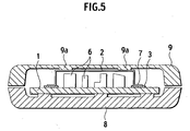
- Fig. 5 shows the shield case 2 covered by a housing 9, and the electronic parts 6 are normally used in this state.
- the shield case 2 pressed against the housings 8 and 9 can allow the flange 7 to be grounded to the metallic ground line 3 by elastic deformation of the flange 7.
- the shield case 2 is pressed in its ceiling portion by a convex portion 9a provided on an internal plane of the housing 9.
- Figs. 6A to 6C are explanatory views for explaining a motion of the flange 7 at the time when the shield case 2 is pressed by the convex portion 9a.
- Fig. 6A shows the shield case 2 mounted on the circuit board 1 at the time before the shield case 2 is pressed by the housing 9.
- the flange 7 is in a state where its tip is allowed to contact with the metallic ground line 3 and its base portion is allowed to be distant from the metallic ground line 3 by a distance "d".
- Fig. 6B shows the shield case 2 pressed by the housing 9.
- the flange 7 is in a state where the entire portion ranging from the tip of the shield case 2 to the base portion thereof is allowed to contact with the metallic ground line 3.
- Fig. 6C shows a state where the housing 9 is detached and pressing of the shield case 2 is relieved.
- the flange 7 restores to its original state of Fig. 6A.
- the flange 7 is hyper-elastic, the flange 7 is never broken down and deformed permanently. Therefore, by attaching and detaching the housings 8 and 9, the shield case 2 can be easily fitted to the circuit board 1 and easily detached from the circuit board 1.
- the shield case 2 is manufactured from metallic materials having a value of the fracture strength ( ⁇ f) /elastic constant (E) , which is about 0.01 or more.
- the shield case 2 having a thickness from 0.1 to 0.3 mm which has commonly been used by manufactures, is shaped by selecting these metallic materials, it has been found that cracks are produced at the bending R portion when bending is performed for the flange 7 having a width of 1 mm.
- the shield case 2 can be manufactured by cutting a block material, such manufacturing of the shield case 2 is inefficient.
- the metallic material used in the shield case 2 and the flange 7 of the present invention are scattered in value in the range of ⁇ f/E > 0.01 (which is illustrated by the slanted lines in Fig. 7). It is therefore possible to utilize a deformation due to viscous flowing on the atomic level, which is different from the plastic deformation, by manufacturing the shield case 2 from these metallic materials.
- forming of the flange 7 having a high dimensional precision without a spring-back can be achieved without causing cracks at the bending R portion.
- Ni-Nb-Zr-Ti alloy, Cu-Zr-Ti-Be alloy, Cu-Zr-Ti alloy, Zr-Cu-Ni-Al alloy (metallic glass), Mg glass, ⁇ -Ti alloy and the like are mentioned.
- Metallic materials having a small spring constant are more advantageous for forming the acute flange 7 having a very small flare. Accordingly, the reason why the metallic materials applied to the present invention are limited will be described.
- Fig. 8 shows a graph showing an elastic deformation curve (stress-strain curve) of metallic materials. Since many of the aforementioned structural metallic materials including stainless, titanium, phosphorbronze, andaluminumalloyexhibit only slight elastic strains, they will be permanently deformed.
- the circle represents an elastic limit point.
- Thesemetallicmaterials can provide sufficiently larger elastic deformations than those of the above-described structural metallic materials.
- a shield case 20 (comparative example) having a thickness of 0.1 to 0.3 mm was made of the aforementioned structural metallic material.
- the shield case 20 has a needle-shaped elastic springs 21, each of which sticks out by 1 mm, in its periphery portion. As shown in Fig. 9A, if the elastic springs 21 is formed to be radial-shaped, the shield case 20 can obtain only a slight spring displacement or permanently deforms before the spring displacement is obtained.
- a shield case 30 (comparative example) was also made.
- the shield case 30 has sufficiently long L-shaped elastic springs 31 instead of the needle-shaped elastic springs 21. With the formation of the L-shaped elastic springs 31, a sufficient displacement is obtained even by the aforementioned structural metallic materials without the permanent deformation. In this case, the requirement for the high density grounding interval is not satisfied.
- the shield case 2 is made of metallic material or metallic glass satisfying ⁇ f/E ⁇ 0.01, it is possible to easily realize the hyper-elastic band-shaped flange 7 having a flare width of not more than 1 mm.
- the shield case 2 is formed so that the flange 7 has a flange width of not more than 1 mm.
- a plurality of shield cases that is, shield cases 2S, 2M and 2L are often arranged adjacently for respective function regions of the circuit board 1.
- a joint margin of 1 mm which is necessary for solder joint, is already achieved, and the interval "t" between the adjacent two shield cases is narrowed down to 2 mm.
- the flare width of the flange 7 being not less than 1 mm is never permitted considering the restriction of space on the circuit board 1. Specifically, this flare width provides no advantage unless it is not greater than 1 mm.
- the shield case 2 By making the shield case 2 from metallic material or metallic glass satisfying ⁇ f/E ⁇ 0.01, the shield case 2 having the flange 7 with the flange width being not more than 1 mm can be made satisfactorily.
- At least one cut 10 should be preferably provided along the direction of the flare width.
- a spring constant of the flange 7 can be controlled by the number of cuts 10. Therefore, it is possible to make the grounding of the shield case 2A (flange 7) and the metallic ground line 3 perfectly. Further, it is possible to achieve easiness in attachment and detachment of the housings 8 and 9 for housing the circuit board 1 and the shield case 2A.
- the flange 7 should be preferably formed to have a nonlinear external periphery portion 11.
- the external periphery portion 11 is not limited to one shaped with simple non-straight lines (wave form) as illustrated in Fig. 12, but the external periphery portion 11 may be a geometric pattern.
- the flange 7 may have a space structure in which a circumferential length of the flange contacting with the metallic ground line 3 is long.
- the circumferential length of the external periphery portion 11 is long by forming the external periphery portion 11 to be shaped with non-straight lines. Therefore, a frictional force exerted between the and the metallic ground line 3 becomes large, and lateral sliding of the flange 7 can be prevented, and then positioning of the shield case 2B is achieved.
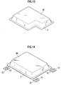
- the shield case 2C illustrated in Fig. 13 has an asymmetrical shape as a whole, and can be easily made by adopting metal or metallic glass, each satisfying ⁇ f/E ⁇ 0.01. Further, as a matter of course, the shield case 2C can be made when the shield case 2C has a dome shape or another shape.
- the shield case 2D illustrated in Fig. 14 has fixing pieces 12 in the flange 7, which are formed to protrude to the outside, and a hole 13 for positioning the shield case 2D with the circuit board 1 is provided in each fixing piece 12.
- the shield case 2D can be fixed to the circuit board 1 by allowing a screw to pass through the hole 13.
- An adhesive tape 14 is adhered to the ceiling of the shield case 2E illustrated in Fig. 15, and the shield case 2E is positioned by fixing the adhesive tape 14 to the housing 9.
- the shield case 2F illustrated in Fig. 16 forms a large number of uneven portions 15 on the ceiling to make the area of the surface larger.
- the shield case 2F has a role to radiate heat effectively from the electronic parts 6 such as a power amplifier covered with the shield case 2F.
- Fig. 17 shows another example of the method of positioning the shield case 2.
- the positioning of the shield case 2 is performed by a concave 16 corresponding to the ceiling portion of the shield case 2, which is provided on the housing 9 side.
- the shield case 2 is pressed by the housings 8 and 9 with the ceiling portion fitted in the concave 16.
- the shield case 2 is made by pressure forming in a supercooled liquid temperature region of the metallic glass.
- the electromagnetic wave shield case is made by warm pressing in a temperature region defined inbetween a glass transition temperature of the metallic glass and a crystallization temperature thereof.
- the metallic glass according to this embodiment is a zirconium base alloy having amorphous structure.
- the electromagnetic wave shield case is made in a supercooled liquid temperature region in which an amorphous structure can be maintained, and under the circumference where a temperature condition, in which a temperature does not reach a crystallization temperature which is an upper limit losing the amorphous structure.
- a deep drawing forming using a die is performed on a foil material made of 55Zr-30Cu-5Ni-10Al (the number symbols represent an atomic ratio) metallic glass having a thickness of 0.1 mm, which is obtained by a single roller method or the like.
- the aforementioned electromagnetic wave shield case according to this embodiment shield case 2, etc. Since it is necessary to suppress the generation and growth of a crystal nucleus during the course of cooling the liquid in order to supercooled liquid, a selection on the aforementioned temperature condition has to be made.
- the single roller method is a method of manufacturing a metallic foil, in which alloy is dissolved by use of an electric furnace or a high-frequency furnace, melted alloy is allowed to be ejected from a tip hole of a crucible by gas pressure. The ejected alloy is contacted to a surface of a rotating cooling rotator to be solidified thereon.
- various forming methods represented by a die casting method and a high pressure injection molding method can be selected without limitation to the method in which the foil material made by the single roller method.
- the flange formability means whether the flange having a width of 0.7 mm can be formed without producing cracks.
- Good means an effective shield amount SE for high frequencies ranging from 0.1 to 6 GHz satisfies SE ⁇ -60 dB.
- With Problem means the effective shield amount SE satisfies -60dB ⁇ SE ⁇ -30dB.
- Bod means the effective shield amount SE satisfies -30dB ⁇ SE.
- the type of a shield case of Embodiments 1 to 8 is same as the shield case 2 shown in Fig. 3.
- the shield case 2 has the following structure. Specifically, the length in the longitudinal direction is 33 mm, the length in the lateral direction is 23 mm, and the thickness is 0.1 mm. Further, the shield case has the flange 7 of 0.7 mm width integrally formed therewith in its lowermost periphery.
- the shield cases of Embodiments 1 to 7 were made by performing warm pressing at the supercooled liquid temperature region for the foil material made of metallic glass (the zirconium base alloy having amorphous structure), which was made by the single roller method.
- the shield case of Embodiment 8 was made from the foil material made of the ⁇ -Ti alloy by use of the deep drawing forming.
- the needle-shaped elastic springs 21 are formed by sheet metal processing method at intervals of 1 mm as in the case of the shield case 20 shown in Fig. 9A. Because it is impossible to form the flange integrally within the shield case 20 unlike in the case of the shield case 2 shown in Fig. 3.
- the shield performance was measured by use of a measurement apparatus 40 shown in Fig. 18.
- the measurement apparatus 40 comprises a radiowave dark room 42 covered with a casing 41, a transmitting antenna 43 and a receiving antenna 44, which are provided to be opposite to each other.
- a circuit board 45 having a hole 45a is located between the transmitting antenna 43 and receiving antenna 44 in the radiowave dark room 42.
- a tested shield case A is located in the radiowave dark room 42 so as to cover the hole 45a.
- the measurement apparatus 40 comprises a network analyzer 46 and a signal circuit 47.
- the network analyzer 46 controls high frequencies radiated from the transmitting antenna 43, and acquires high frequencies leaking from the tested shield case A through the receiving antenna 44 to measure them.
- the shield case in measuring the shield performance, was pressed to the circuit board 45 to be fixed thereto within the displacement of 0.5 mm of the flange 7.
- the shield case was slightly pressed to the circuit board 45 to be fixed thereto within a range where spring pieces were deformed permanently and were not broken down.
- the shield case 2 is made of metallic material or metallic glass having the value (ratio) of about 0.01 or more (not less than 0.01) expressed by the fracture strength( ⁇ f)/elastic constant(E).
- the plurality of shield case 2 (for example, the shield case 2S, 2M and 2L, shown in Fig, 10) , which is adj acent to each other more densely than the conventional solder joint, can be arranged.
- the flange 7 can obtain a large displacement which is necessary to obtain a reliable shield, i.e., an electrical connection. Therefore, according to the shield case of this embodiment, it is possible to obtain a good shield performance for shielding electromagnetic waves.
- the through hole which has been heretofore necessary, is unnecessary. Therefore, the shield case 2 is easily attached to and detached from the circuit board 1.
- the shield case 2 is fitted to the circuit board 1, complicated processes are not required, and the shield case 2 is cheap.
- the shield case 2 is easily used as a recycled product.
- the shield case according to this embodiment is made of metallic materials having the value (ratio) of about 0.01 or more (not less than 0.01) expressed by the fracture strength(of)/elastic constant (E) , it is possible to utilize a deformation due to viscous flowing on the atomic level, which is different from a plastic deformation. Thus it is possible to form a high precision flange without a spring-back.
- the electromagnetic wave shield case having the hyper-elastic flange integrally formed therewith can be provided, which needs no through hole and is capable of securing a large elastic spring displacement while decreasing the occupied area for grounding.
- the interval between the two shield cases adjacent to each other can be narrowed to 2 mm at most.
- the spring constant of the flange 7 can be controlled by the number of cuts 10. It is therefore possible to make the grounding of the flange 7 and the metallic ground line 3 perfectly. Further, it is possible to achieve easiness in attachment and detachment of the housings 8 and 9 for housing the circuit board 1 and the shield case 2A.
- the circumferential length of the flange 7 is long by forming the external periphery portion 11 of the flange 7 to be shaped with nonlinear lines. Therefore, the frictional force exertedbetween the flange 7 and the metallic ground line 3 (grounding conduction portion) becomes large, and lateral sliding of the flange 7 can be prevented.
- the shield case is made of metallic glass, it is possible to form high precision flange without a spring-back.
- the electromagnetic wave shield case having the hyper-elastic flange integrally formed therewith can be provided. Further, the electromagnetic wave shield case, which needs no through hole, and is capable of securing a large elastic spring displacement, which has not been heretofore present, can also be provided, while decreasing the occupied area for grounding.
- various forming methods represented by a die casting method and a high pressure injection molding method can be selected without limitation to the method in which the foil material is deep-drawn using the single roller method.
- the shield case which has a dome shape, other shapes including a nonsymmetrical shape, or which has the flange having an external periphery portion with nonlinear lines, without limitation of the shape of the shield case to the box shape.
- An objective of the present invention is to form a hyper-elastic flange integrally within a shield case body around a periphery thereof while decreasing an occupied area for grounding.
- the shield case 2 according to the present invention is disposed to cover electronic parts 6 on a circuit board 1, and which has a flange 7 formed integrally therewith so as to contact with a metallic ground line 3 on the circuit board 1.
- the flange 7 is elastically deformed to be grounded, thus a leakage of electromagnetic waves to the outside of the shield case 2 is prevented.
- the flange 7 is made of metallic glass. By forming the flange 7 from metallic glass, a displacement due to viscous flowing on the atomic level, which is different from a plastic deformation, can be utilized, and thus a high precision flange can be formed without a spring-back.
Abstract
Description
- The present invention relates to an electromagnetic wave shield case disposed to cover electronic parts on a circuit board (printed circuit board) used for a cellular phone and a computer, and an electromagnetic wave shield case manufacturing method.
- When electronic parts such as an oscillator for generating electromagnetic waves are present on a circuit board, preventing influence on other circuit devices due to electromagnetic waves is required.
- Specifically, in order to prevent occurrence of radiation noise, technologies have been identified that shielding the electronic parts so as not to propagate generated electromagnetic waves to the outside by surrounding the electronic parts with an electromagnetic wave shield case essentially made of metallic materials, which are of a conductive substance.
- When such an electromagnetic wave shield case (hereinafter referred to as "shield case" when appropriate) is located on the circuit board, as shown in Fig.1, a metallic ground line 3 (portion conducted to the earth ("grounding conduction portion", hereinafter)) is provided in a region on a
circuit board 1 corresponding to the lowermost portion of ashield case 50A and around it. Themetallic ground line 3, and the lowermost portion of theshield case 50A, or part of the lowermost portion thereof are joined by soldering, and a solderingjoint portion 4 is formed. - However, joining of the
shield case 50A to themetallic ground line 3 by soldering has the following problems. That is, in a solder joining method, the following problems can be enumerated: - (a) adverse affects, which include deformation and partial breakage of the printed circuit board and electronic parts due to heating when soldering;
- (b) an inefficient job of removing soldering from the
shield case 50A when theshield case 50A on thecircuit board 1 is used as a recycled product after its validity has expired; - (c) a troublesome job of performing treatments such as washing before and after the soldering is performed;
- (d) fluxes, dispersal of soldering, and sticking of dispersed soldering on circuit elements at the stage of soldering; and
- (e) the necessity to remove the soldering and detach the
shield case 50A when electronic parts within theshield case 50A are replaced. Accordingly, various technologies have been heretofore proposed.Prior Art # 1 solves the problem (e), and according to thePrior Art # 1, as shown in Fig. 2, a truss-shaped frame 5 is joined to themetallic ground line 3 by soldering, and a so called two-piecetype shield case 50B in which the truss-shaped frame 5 and a detachableupper cover 60 are combined. -
-
Prior Art # 2, which was developed by the Inventors of this application, solves the problems (a) to (e), whereby a shield case, in which an anchor pin integrally united thereto without soldering and has bending elasticity, is elastically joined to a through hole provided in a circuit board (for example, Japanese Patent Application Laid-open No. 2003-179378). -
Prior Art # 3 was also developed by the Inventors of this application to solve the problems (a) to (e). According to PriorArt # 3, a lock pin having bending elasticity, which is integrally united with a back surface of a shield case without soldering, is elastically jointed to a housing for a circuit board. InPrior Art # 3, a structure, in which part of the lowermost end of the shield case is made conductive by allowing the part to contact with a metallic ground line, is adopted (for example, Japanese Patent Application Laid-open No. 2003-179379). - Zr group amorphous alloy (metallic glass) having high amorphous forming ability as well as high strength and ductility, which has been developed by the Inventors of this application, has also been known (for example, Japanese Patent Application Laid-open Nos. 2000-129378 and 2000-178700).
- However,
Prior Art # 1 has a problem in that the height of theshield case 50B is apt to be high, and a reduction in the thickness of thecircuit board 1 is disturbed, resulting in a high cost of manufacturing. - In cellular phones and computers in which the thickness has become rapidly thinner, limitations with respect to their spaces are brought due to the layout of electronic parts. Further, electronic parts may be mounted on the back face of a circuit board due to diffusion of a double-sidedmount board. Therefore, provisioning of the number of through holes, which is necessary and sufficient, on a circuit board has come to be no longer permitted, and a new problem in that
Prior Art # 2 cannot be applied is occurring. - Although
Prior Art # 3 does not require provision of a through hole in a circuit board, PriorArt # 3 has the following new problem regarding realization of a reliable electric connection of the shield case and the metallic ground line. - Specifically, in order to absorb distortion of the housing and the circuit board (printed circuit board) made thinner, and to realize the electric connection of the shield case and the metallic ground line with high reliability, it is necessary to make the elastic spring displacement of the shield case larger.
- Further, since a frequency band used for radio communications begins to have higher frequency, a grounding interval for the shield case and the metallic ground line is required to be shorter.
- In order to meet these two requirements, in
Prior Art # 3, while being restricted with respect to the space required for grounding of the shield case, the grounding interval for the shield case and the metallic ground line will be made extremely short. Therefore, in a conventional sheet metal processing method used after the metal is press-punched, in which the metal is formed by bending, a new problem arises in that design of the shield case has become difficult. - Specifically, design of the shield case which meets the requirements including mass productivity by press-punching and bend-forming, the shorter grounding interval, a decrease in the occupied area for grounding, and provision of a large elastic spring displacement, becomes extremely difficult.
- In order to manufacture the shield case, in a conventional method in which a crystalline metallic material is formed by bending or deep drawing by means of a plastic deformation, there is a limit in securing a sufficient elastic deformation while keeping the flare width and the bending radius of the shield case small.
- In order to solve not only the conventional problems (a) to (e) but also the new problems related to
Prior Art # 1 to #3, an objective of the present invention is to provide an electromagnetic wave shield case and an electromagnetic wave shield case manufacturing method, which needs no through hole and is capable of securing a large elastic spring displacement while decreasing an occupied area for grounding. - As a result of examinations, the Inventors of this application acquired the knowledge that a high precision flange can be formed without a spring-back by use of a deformation due to viscous flowing on the atomic level, which is different from a plastic deformation,using metallic glass. The inventors then accomplished the present invention base on the knowledge.
- In order to achieve the objective, a first aspect of the present invention is an electromagnetic wave shield case (2) comprising a shield case body (2) configured to cover electronic parts (6) on a circuit board (1) and a flange (7) formed integrally with said shield case body (2) , characterized by said shield case body (2) and said flange (7) are made of metallic material having a value of 0.01 or more expressed by a fracture strength/elastic constant, and said flange (7) is elastically deformed to be grounded to an grounding conduction portion (3) on said circuit board (1) to prevent a leakage of electromagnetic waves to outside of said electromagnetic wave shield case (2).
- Herein, the fracture strength means one defined by a yield stress in a mechanical strength test or a stress which is an elastic limit. The elastic constant is one defined by a proportionality constant with respect to a stress and a strain within the elastic limit.
- According to the first aspect of the present invention, since the electromagnetic wave shield case is made of the metallic material having the value of 0.01 or more expressed by a fracture strength/elastic constant, a deformation due to viscous flowing on the atomic level which is different from a plastic deformation can be utilized, and thus a high precision flange can be formed without a spring-back.
- A second aspect of the present invention is the electromagnetic wave shield case according to the first aspect, wherein said flange (7) has a flare width of 1 mm or less (not more than 1 mm).
- A third aspect of the present invention is the electromagnetic wave shield case according to the second aspect, wherein said flange (7) has at least one cut (10) along a direction of said flare width.
- A fourth aspect of the present invention is the electromagnetic wave shield case according to the first through third aspects, wherein said flange (7) has a nonlinear external periphery portion (11).
- A fifth aspect of the present invention is an electromagnetic wave shield case (2) comprising a shield case body (2) configured to cover electronic parts (6) on a circuit board (1) and a flange (7) formed integrally with said shield case body (2), characterized by said shield case body (2) and said flange (7) are made of metallic glass, and said flange (7) is elastically deformed to be grounded to an grounding conduction portion (3) on said circuit board (1) to prevent a leakage of electromagnetic waves to outside of said electromagnetic wave shield case (2).
- According to the fifth aspect of the present invention, since the electromagnetic wave shield case is manufactured using metallic glass, it is possible to utilize a deformation due to viscous flowing on the atomic level which is different from a plastic deformation, and thus a high precision flange can be formed without a spring-back.
- A sixth aspect of the present invention is the electromagnetic wave shield case according to the fifth aspect, wherein said flange (7) has a flare width of 1 mm or less (not more than 1 mm).
- A seventh aspect of the present invention is the electromagnetic wave shield case according to the sixth aspect, wherein said flange (7) has at least one cut (10) along a direction of said flare width.
- An eighth aspect of the present invention is the electromagnetic wave shield case according to the fifth through seventh aspects, wherein said flange (7) has a nonlinear external periphery portion (11).
- A ninth aspect of the present invention is the electromagnetic wave shield case according to the fifth through eighth aspects, wherein said metallic glass is a zirconium base alloy having amorphous structure.
- A tenth aspect of the present invention is a method for manufacturing an electromagnetic wave shield case (2) according to claim 5-9, wherein said electromagnetic wave shield case is made by pressure forming in a supercooled liquid temperature region of said metallic glass to be used for said electromagnetic wave shield case.
- An eleventh aspect is a method for manufacturing an electromagnetic wave shield case (2) according to claim 5-9, wherein said electromagnetic wave shield case is made by warm pressing in a temperature region defined inbetween a glass transition temperature and a crystallization temperature of said metallic glass to be used for said electromagnetic wave shield case.
- A twelfth aspect of the present invention is the method according to the tenth or eleventh aspects, wherein saidmetallic glass is a zirconium base alloy having amorphous structure.
- According to such aspects, various forming methods represented by a die casting method and a high-pressure inj ection molding method can be selected without limits to the method of performing a deep drawing forming for a foil material using a single roller method.
- Thus, it is possible to easily mold the shield case and the like, which has a dome shape, other shapes including a nonsymmetrical shape, or which has a flange having an external periphery portion with non-straight lines.
-
- Fig. 1 is a view showing a state where a conventional electromagnetic wave shield case is grounded;
- Fig. 2 is a view showing a state where another conventional electromagnetic wave shield case is grounded;
- Fig. 3 is a schematic perspective view showing an electromagnetic wave shield case equipped with a circuit board according to an embodiment of the present invention;
- Fig. 4 is a schematic sectional view taken along the line IV-IV of Fig. 3;
- Fig. 5 is a view showing the electromagnetic wave shield case sandwiched by upper and lower housings in the sectional view taken along the line IV-IV of Fig. 3;
- Fig. 6A is a view showing the electromagnetic wave shield case mounted on the circuit board at the time before it is pressed by the housings;
- Fig. 6B is a view showing the electromagnetic wave shield case pressed by the housings;
- Fig. 6C is a view showing a state where the housings are detached and pressing of the shield case is relieved;
- Fig. 7 is a graph showing a relation between the fracture strength of metallic materials and the elastic constant thereof;
- Fig. 8 is a graph showing a relation between the stress of the metallic materials and the strain thereof;
- Figs. 9A and 9B are perspective views of an electromagnetic wave shield case according to a comparative example;
- Fig. 10 is a schematic perspective view showing an arrangement example of the electromagnetic wave shield case on the circuit board;
- Fig. 11 is a partial perspective view of the electromagnetic wave shield case according to another embodiment of the present invention;
- Fig. 12 is a partial perspective view of the electromagnetic wave shield case according to another embodiment of the present invention;
- Fig. 13 is a perspective view of the electromagnetic wave shield case according to another embodiment of the present invention;
- Fig. 14 is a perspective view of the electromagnetic wave shield case according to another embodiment of the present invention;
- Fig. 15 is a perspective view of the electromagnetic wave shield case according to another embodiment of the present invention;
- Fig. 16 is a partial perspective view of the electromagnetic wave shield case according to another embodiment of the present invention;
- Fig. 17 is a schematic section view showing a method of positioning the electromagnetic wave shield case according to another embodiment of the present invention; and
- Fig. 18 is an explanatory view of a measurement system for the shield performance.
-
- Embodiments of the present invention will be described below. Note that the same components as those in Figs. 1 and 2 are denoted by the same reference numeral and symbols, and descriptions for them are omitted.
- Figs. 3 and 4 show a
shield case 2 shielding electromagnetic wave according to an embodiment of the present invention. Theshield case 2 is disposed to coverelectronic parts 6 on acircuit board 1. Aflange 7 formed integrally with the shield case 2 (shield case body) , which is elastically deformed to be grounded to a metallic ground line 3 (grounding conduction portion) on thecircuit board 1, so that leakage of electromagnetic waves to the outside of theshield case 2 is prevented. - The
flange 7 is manufactured integrally with theshield case 2. Theshield case 2 and theflange 7 are made of metallic material having a value (ratio) of about 0.01 or more (not less than 0.01) expressed by a fracture strength(σf)/elastic constant(E). - Further, in this embodiment, the
shield case 2 and theflange 7 are made of metallic material having a value of the fracture strength (σf) /elastic constant (E) is about 0.1 or less. In other words, the value of the fracture strength (σf /elastic constant(E) for theshield case 2 and theflange 7 is in the range of 0.01 ≤ σf/E ≤ 0.1. - It is preferable that a value of σf/E for the
shield case 2 and theflange 7 is in the range of 0.01 ≤ of/E ≤ 0.05. - Specifically, the
shield case 2 is formed of a thinmetallic foil, and the band-shapedflange 7, having a small width, is formed over the entire circumference of an open end of theshield case 2. Theshield case 2 is placed on themetallic ground line 3 of thecircuit board 1 housed within ahousing 8 of an electronic device. - The
shield case 2 can be manufactured by, for example, 55Zr-30Cu-5Ni-10Al alloy (the number symbols represent an atomic ratio). However, the material of theshield case 2 is not always limited to the alloy (metallic material). The material of theshield case 2 may be metallic material having the value (ratio) of about 0.01 or more expressed by the fracture strength(σf)/elastic constant(E). - Herein, the fracture strength(σf) means one defined by a yield stress in a mechanical strength test or a stress which is an elastic limit. The fracture strength (σf) can be measured in accordance with JIS Z2241. The elastic constant(E) means a Young's modulus defined by a proportionality constant with respect to a stress and a strain within the elastic limit. For example, the elastic constant (E) can be measured by the method described in "Engineering Materials / An introduction to their properties and applications", M. F. Ashby and D. R. H. Jones, Cambridge University, England Pergamon Press.
- The
shield case 2 floats by spring of theflange 7 having an angle (see Fig. 4). In this state, there is a possibility of having a portion where themetallic ground line 3 and theflange 7 may not be connected electrically due to deflection of thecircuit board 1. - Fig. 5 shows the
shield case 2 covered by ahousing 9, and theelectronic parts 6 are normally used in this state. Theshield case 2 pressed against thehousings flange 7 to be grounded to themetallic ground line 3 by elastic deformation of theflange 7. Theshield case 2 is pressed in its ceiling portion by aconvex portion 9a provided on an internal plane of thehousing 9. - Figs. 6A to 6C are explanatory views for explaining a motion of the
flange 7 at the time when theshield case 2 is pressed by theconvex portion 9a. Fig. 6A shows theshield case 2 mounted on thecircuit board 1 at the time before theshield case 2 is pressed by thehousing 9. Theflange 7 is in a state where its tip is allowed to contact with themetallic ground line 3 and its base portion is allowed to be distant from themetallic ground line 3 by a distance "d". - Fig. 6B shows the
shield case 2 pressed by thehousing 9. Theflange 7 is in a state where the entire portion ranging from the tip of theshield case 2 to the base portion thereof is allowed to contact with themetallic ground line 3. - Fig. 6C shows a state where the
housing 9 is detached and pressing of theshield case 2 is relieved. Theflange 7 restores to its original state of Fig. 6A. As described above, since theflange 7 is hyper-elastic, theflange 7 is never broken down and deformed permanently. Therefore, by attaching and detaching thehousings shield case 2 can be easily fitted to thecircuit board 1 and easily detached from thecircuit board 1. - In order to realize the above describedmotion of the
shield case 2, theshield case 2 is manufactured from metallic materials having a value of the fracture strength (σf) /elastic constant (E) , which is about 0.01 or more. - Specifically, as shown in Fig. 7, when a relation between the fracture strength (σf) and the elastic constant (E) is observed on the graph, many of the structural metal materials such as stainless, titanium and aluminum alloy are scattered in value within a range of σf/E < 0.01.
- In a case where the
shield case 2 having a thickness from 0.1 to 0.3 mm, which has commonly been used by manufactures, is shaped by selecting these metallic materials, it has been found that cracks are produced at the bending R portion when bending is performed for theflange 7 having a width of 1 mm. As a matter of course, though theshield case 2 can be manufactured by cutting a block material, such manufacturing of theshield case 2 is inefficient. - Contrary to this, the metallic material used in the
shield case 2 and theflange 7 of the present invention are scattered in value in the range of σf/E > 0.01 (which is illustrated by the slanted lines in Fig. 7). It is therefore possible to utilize a deformation due to viscous flowing on the atomic level, which is different from the plastic deformation, by manufacturing theshield case 2 from these metallic materials. - Thus, forming of the
flange 7 having a high dimensional precision without a spring-back can be achieved without causing cracks at the bending R portion. Exemplifying the metallic materials of the present invention, Ni-Nb-Zr-Ti alloy, Cu-Zr-Ti-Be alloy, Cu-Zr-Ti alloy, Zr-Cu-Ni-Al alloy (metallic glass), Mg glass, β-Ti alloy and the like are mentioned. - Metallic materials having a small spring constant are more advantageous for forming the
acute flange 7 having a very small flare. Accordingly, the reason why the metallic materials applied to the present invention are limited will be described. - Fig. 8 shows a graph showing an elastic deformation curve (stress-strain curve) of metallic materials. Since many of the aforementioned structural metallic materials including stainless, titanium, phosphorbronze, andaluminumalloyexhibit only slight elastic strains, they will be permanently deformed. The elastic strain ε is a natural logarithm of a quantity obtained by dividing an elastic deformation ΔS, which is caused by adding an external force, with an original length S, and expressed by ε = Ln (ΔS/S). In Fig. 8, the circle represents an elastic limit point.
- Contrary to the above-described case, the metallic materials in the present invention are scattered in values within the range σf/E > 0.01, that is, a range being delimited by and lower than the slope σ-ε corresponding to σf/E = 0.01 (shown with slant lines in Fig. 8). Thesemetallicmaterials can provide sufficiently larger elastic deformations than those of the above-described structural metallic materials.
- Herein, as shown in Fig. 9A, a shield case 20 (comparative example) having a thickness of 0.1 to 0.3 mm was made of the aforementioned structural metallic material. The
shield case 20 has a needle-shapedelastic springs 21, each of which sticks out by 1 mm, in its periphery portion. As shown in Fig. 9A, if theelastic springs 21 is formed to be radial-shaped, theshield case 20 can obtain only a slight spring displacement or permanently deforms before the spring displacement is obtained. - On the other hand, as shown in Fig. 9B, a shield case 30 (comparative example) was also made. The
shield case 30 has sufficiently long L-shapedelastic springs 31 instead of the needle-shaped elastic springs 21. With the formation of the L-shapedelastic springs 31, a sufficient displacement is obtained even by the aforementioned structural metallic materials without the permanent deformation. In this case, the requirement for the high density grounding interval is not satisfied. - Contrary to this, since the
shield case 2 is made of metallic material or metallic glass satisfying σf/E ≥ 0.01, it is possible to easily realize the hyper-elastic band-shapedflange 7 having a flare width of not more than 1 mm. - It is preferable that the
shield case 2 is formed so that theflange 7 has a flange width of not more than 1 mm. - As shown in Fig. 10, a plurality of shield cases, that is,
shield cases circuit board 1. In this case, a joint margin of 1 mm, which is necessary for solder joint, is already achieved, and the interval "t" between the adjacent two shield cases is narrowed down to 2 mm. At this time, the flare width of theflange 7 being not less than 1 mm is never permitted considering the restriction of space on thecircuit board 1. Specifically, this flare width provides no advantage unless it is not greater than 1 mm. - By making the
shield case 2 from metallic material or metallic glass satisfying σf/E ≥ 0.01, theshield case 2 having theflange 7 with the flange width being not more than 1 mm can be made satisfactorily. - As a
shield case 2A shown in Fig. 11, at least one cut 10 should be preferably provided along the direction of the flare width. - With such a constitution, a spring constant of the
flange 7 can be controlled by the number ofcuts 10. Therefore, it is possible to make the grounding of theshield case 2A (flange 7) and themetallic ground line 3 perfectly. Further, it is possible to achieve easiness in attachment and detachment of thehousings circuit board 1 and theshield case 2A. - In a
shield case 2B shown in Fig. 12, theflange 7 should be preferably formed to have a nonlinearexternal periphery portion 11. Theexternal periphery portion 11 is not limited to one shaped with simple non-straight lines (wave form) as illustrated in Fig. 12, but theexternal periphery portion 11 may be a geometric pattern. Further, theflange 7 may have a space structure in which a circumferential length of the flange contacting with themetallic ground line 3 is long. - In this structure, the circumferential length of the
external periphery portion 11 is long by forming theexternal periphery portion 11 to be shaped with non-straight lines. Therefore, a frictional force exerted between the and themetallic ground line 3 becomes large, and lateral sliding of theflange 7 can be prevented, and then positioning of theshield case 2B is achieved. - Moreover, modifications of the
shield case 2 are illustrated in Figs. 13 to 16. It is natural that any of these shield cases belongs to the present invention. - The shield case 2C illustrated in Fig. 13 has an asymmetrical shape as a whole, and can be easily made by adopting metal or metallic glass, each satisfying σf/E ≥ 0.01. Further, as a matter of course, the shield case 2C can be made when the shield case 2C has a dome shape or another shape.
- The
shield case 2D illustrated in Fig. 14 has fixingpieces 12 in theflange 7, which are formed to protrude to the outside, and ahole 13 for positioning theshield case 2D with thecircuit board 1 is provided in each fixingpiece 12. Theshield case 2D can be fixed to thecircuit board 1 by allowing a screw to pass through thehole 13. - Furthermore, it is also possible to position the
shield case 2D by inserting a protrusion (not shown) into thehole 13 provided in thecircuit board 1 or the housing 8 (or the housing 9). - An
adhesive tape 14 is adhered to the ceiling of theshield case 2E illustrated in Fig. 15, and theshield case 2E is positioned by fixing theadhesive tape 14 to thehousing 9. - The
shield case 2F illustrated in Fig. 16 forms a large number ofuneven portions 15 on the ceiling to make the area of the surface larger. Theshield case 2F has a role to radiate heat effectively from theelectronic parts 6 such as a power amplifier covered with theshield case 2F. - Fig. 17 shows another example of the method of positioning the
shield case 2. The positioning of theshield case 2 is performed by a concave 16 corresponding to the ceiling portion of theshield case 2, which is provided on thehousing 9 side. Theshield case 2 is pressed by thehousings - Next, a method of manufacturing the electromagnetic wave shield case will be described.
- In the method of manufacturing the electromagnetic wave shield case, for example, the
shield case 2 is made by pressure forming in a supercooled liquid temperature region of the metallic glass. - In other words, in this method, the electromagnetic wave shield case is made by warm pressing in a temperature region defined inbetween a glass transition temperature of the metallic glass and a crystallization temperature thereof.
- The metallic glass according to this embodiment is a zirconium base alloy having amorphous structure.
- To be precise, the electromagnetic wave shield case is made in a supercooled liquid temperature region in which an amorphous structure can be maintained, and under the circumference where a temperature condition, in which a temperature does not reach a crystallization temperature which is an upper limit losing the amorphous structure.
- A deep drawing forming using a die is performed on a foil material made of 55Zr-30Cu-5Ni-10Al (the number symbols represent an atomic ratio) metallic glass having a thickness of 0.1 mm, which is obtained by a single roller method or the like.
- By such method, the aforementioned electromagnetic wave shield case according to this embodiment (
shield case 2, etc) is made. Since it is necessary to suppress the generation and growth of a crystal nucleus during the course of cooling the liquid in order to supercooled liquid, a selection on the aforementioned temperature condition has to be made. - Herein, the single roller method is a method of manufacturing a metallic foil, in which alloy is dissolved by use of an electric furnace or a high-frequency furnace, melted alloy is allowed to be ejected from a tip hole of a crucible by gas pressure. The ejected alloy is contacted to a surface of a rotating cooling rotator to be solidified thereon.
- At this time, if forming is performed at the supercooled liquid temperature region, various forming methods represented by a die casting method and a high pressure injection molding method can be selected without limitation to the method in which the foil material made by the single roller method.
- Table below shows results obtained by comparing the formability of the flange, the obtained maximum displacement and the shield performance as to the shield case of the embodiments and the comparison examples.
Shield Case Material σ f/E Flange Formability Max Displacement (mm) Shield Performance Remarks Embodiment 1 55Zr-30Cu-5Ni-10Al 0.019 Good Not less than 0.5 Good Embodiment 2 52Zr-17Cu-16Ni-10Al-5Ti 0.021 Good Not less than 0.5 Good Embodiment 3 52Zr-17Cu-16Ni-10Al-4Ti-1Nb 0.019 Good Not less than 0.5 Good Embodiment 4 60Zr-20Cu-10Al-10Pd 0.020 Good Not less than 0.5 Good Embodiment 5 50Zr-5Ti-20Cu-5Fe-10Al-5Be 0.021 Good Not less than 0.5 Good Embodiment 6 57Cu-29Zr-10Ti-4Be 0.020 Good Not less than 0.5 Good Embodiment 7 55Ni-20Nb-20Zr-5Ti 0.021 Good Not less than 0.5 Good Embodiment 8 β-Ti Alloy 0.012 Possible Not less than 0.5 Good Comparison 1 SUS304 0.001 Bad 0.1 Bad Alternative Formation of Spring Piece at Intervals of 1 mm Comparison 2 Phosphor Bronze (C51900) 0.007 Bad 0.3 with Problem Comparison 3 7075-T6 Aluminum Alloy 0.008 Bad 0.2 Comparison 4JIS2 class Ti 0.002 Bad 0.1 Bad - The flange formability means whether the flange having a width of 0.7 mm can be formed without producing cracks. In the shield performance, "Good" means an effective shield amount SE for high frequencies ranging from 0.1 to 6 GHz satisfies SE<-60 dB. "With Problem" means the effective shield amount SE satisfies -60dB<SE<-30dB. "Bad" means the effective shield amount SE satisfies -30dB<SE.
- The type of a shield case of
Embodiments 1 to 8 is same as theshield case 2 shown in Fig. 3. Theshield case 2 has the following structure. Specifically, the length in the longitudinal direction is 33 mm, the length in the lateral direction is 23 mm, and the thickness is 0.1 mm. Further, the shield case has theflange 7 of 0.7 mm width integrally formed therewith in its lowermost periphery. - The shield cases of
Embodiments 1 to 7 were made by performing warm pressing at the supercooled liquid temperature region for the foil material made of metallic glass (the zirconium base alloy having amorphous structure), which was made by the single roller method. The shield case ofEmbodiment 8 was made from the foil material made of the β-Ti alloy by use of the deep drawing forming. - As to the shield cases of Comparison Examples 1 to 4, the needle-shaped
elastic springs 21 are formed by sheet metal processing method at intervals of 1 mm as in the case of theshield case 20 shown in Fig. 9A. Because it is impossible to form the flange integrally within theshield case 20 unlike in the case of theshield case 2 shown in Fig. 3. - Moreover, the shield performance was measured by use of a
measurement apparatus 40 shown in Fig. 18. Themeasurement apparatus 40 comprises aradiowave dark room 42 covered with acasing 41, a transmittingantenna 43 and a receivingantenna 44, which are provided to be opposite to each other. - In the
measurement apparatus 40, acircuit board 45 having ahole 45a is located between the transmittingantenna 43 and receivingantenna 44 in theradiowave dark room 42. A tested shield case A is located in theradiowave dark room 42 so as to cover thehole 45a. - The
measurement apparatus 40 comprises anetwork analyzer 46 and asignal circuit 47. Thenetwork analyzer 46 controls high frequencies radiated from the transmittingantenna 43, and acquires high frequencies leaking from the tested shield case A through the receivingantenna 44 to measure them. - Specifically, high frequencies ranging from 0.1 to 6 GHz were transmitted from the transmitting
antenna 43, and the amount of high frequencies leaking to the outside of the tested shield case A was measured through the receivingantenna 44, whereby the shield performance was evaluated. - As to the shield cases of
Embodiments 1 to 8, in measuring the shield performance, the shield case was pressed to thecircuit board 45 to be fixed thereto within the displacement of 0.5 mm of theflange 7. On the other hand, as to the shield cases of Comparison Examples 1 to 4, the shield case was slightly pressed to thecircuit board 45 to be fixed thereto within a range where spring pieces were deformed permanently and were not broken down. - As is clear from the Table, the shield cases of
Embodiments 1 to 8 were capable of obtaining a good effective shield amount SE of -60 dB. However, the shield cases of Comparison Examples 1 to 4 were incapable of achieving sufficient shield effects. (Operation and Effect) - As described above, for the
shield case 2, it is understood how useful theshield case 2 is made of metallic material or metallic glass having the value (ratio) of about 0.01 or more (not less than 0.01) expressed by the fracture strength(σf)/elastic constant(E). - To be precise, according to this embodiment, since the height of the
shield case 2 is low and the flare width of theflange 7 is small. Therefore, the plurality of shield case 2 (for example, theshield case - The
flange 7 can obtain a large displacement which is necessary to obtain a reliable shield, i.e., an electrical connection. Therefore, according to the shield case of this embodiment, it is possible to obtain a good shield performance for shielding electromagnetic waves. - Further, to fit the
shield case 2 to thecircuit board 1, the through hole, which has been heretofore necessary, is unnecessary. Therefore, theshield case 2 is easily attached to and detached from thecircuit board 1. When theshield case 2 is fitted to thecircuit board 1, complicated processes are not required, and theshield case 2 is cheap. Moreover, theshield case 2 is easily used as a recycled product. - Since the shield case according to this embodiment is made of metallic materials having the value (ratio) of about 0.01 or more (not less than 0.01) expressed by the fracture strength(of)/elastic constant (E) , it is possible to utilize a deformation due to viscous flowing on the atomic level, which is different from a plastic deformation. Thus it is possible to form a high precision flange without a spring-back.
- Accordingly, the electromagnetic wave shield case having the hyper-elastic flange integrally formed therewith can be provided, which needs no through hole and is capable of securing a large elastic spring displacement while decreasing the occupied area for grounding.
- According to this embodiment, the interval between the two shield cases adjacent to each other can be narrowed to 2 mm at most. Thus, it is possible to cope with the restriction with respect to space on the
circuit board 1. - According to this embodiment, the spring constant of the
flange 7 can be controlled by the number ofcuts 10. It is therefore possible to make the grounding of theflange 7 and themetallic ground line 3 perfectly. Further, it is possible to achieve easiness in attachment and detachment of thehousings circuit board 1 and theshield case 2A. - According to this embodiment, the circumferential length of the
flange 7 is long by forming theexternal periphery portion 11 of theflange 7 to be shaped with nonlinear lines. Therefore, the frictional force exertedbetween theflange 7 and the metallic ground line 3 (grounding conduction portion) becomes large, and lateral sliding of theflange 7 can be prevented. - According to this embodiment, since the shield case is made of metallic glass, it is possible to form high precision flange without a spring-back.
- Thus, the electromagnetic wave shield case having the hyper-elastic flange integrally formed therewith can be provided. Further, the electromagnetic wave shield case, which needs no through hole, and is capable of securing a large elastic spring displacement, which has not been heretofore present, can also be provided, while decreasing the occupied area for grounding.
- According to the method of manufacturing the electromagnetic wave shield case of the embodiment, various forming methods represented by a die casting method and a high pressure injection molding method can be selected without limitation to the method in which the foil material is deep-drawn using the single roller method. Thus, it is possible to easily mold the shield case, which has a dome shape, other shapes including a nonsymmetrical shape, or which has the flange having an external periphery portion with nonlinear lines, without limitation of the shape of the shield case to the box shape.
- The present invention was described by the embodiments in detail. It is apparent that the present invention is not limited to the embodiments described in the specification of this application. The present invention can be carried out as various modifications without departing from the scope and spirit of the present invention, which is defined by the claims attached. An objective of the present invention is to form a hyper-elastic flange integrally within a shield case body around a periphery thereof while decreasing an occupied area for grounding. The
shield case 2 according to the present invention is disposed to coverelectronic parts 6 on acircuit board 1, and which has aflange 7 formed integrally therewith so as to contact with ametallic ground line 3 on thecircuit board 1. Theflange 7 is elastically deformed to be grounded, thus a leakage of electromagnetic waves to the outside of theshield case 2 is prevented. Theflange 7 is made of metallic glass. By forming theflange 7 from metallic glass, a displacement due to viscous flowing on the atomic level, which is different from a plastic deformation, can be utilized, and thus a high precision flange can be formed without a spring-back.
Claims (12)
- An electromagnetic wave shield case (2) comprising:a shield case body (2) configured to cover electronic parts (6) on a circuit board (1); anda flange (7) formed integrally with said shield case body (2),
characterized by
said shield case body (2) and said flange (7) are made of metallic material having a value of 0.01 or more expressed by a fracture strength/elastic constant, and
said flange (7) is elastically deformed to be grounded to an grounding conduction portion (3) on said circuit board (1) to prevent a leakage of electromagnetic waves to outside of said electromagnetic wave shield case (2). - The electromagnetic wave shield case (2) according to claim 1, wherein said flange (7) has a flare width of 1 mm or less.
- The electromagnetic wave shield case (2A) according to claim 2, wherein said flange (7) has at least one cut (10) along a direction of said flare width.
- The electromagnetic wave shield case (2B) according to claims 1 - 3, wherein said flange (7) has a nonlinear external periphery portion (11).
- An electromagnetic wave shield case (2) comprising:characterized bya shield case body (2) configured to cover electronic parts (6) on a circuit board (1); anda flange (7) formed integrally with said shield case body (2),
said shield case body (2) and said flange (7) are made of metallic glass, and
said flange (7) is elastically deformed to be grounded to an grounding conduction portion (3) on said circuit board (1) to prevent a leakage of electromagnetic waves to outside of said electromagnetic wave shield case (2). - The electromagnetic wave shield case (2) according to claim 5, wherein said flange (7) has a flare width of 1 mm or less.
- The electromagnetic wave shield case (2A) according to claim 6, wherein said flange (7) has at least one cut (10) along a direction of said flare width.
- The electromagnetic wave shield case (2B) according to claims 5-7, wherein said flange (7) has a nonlinear external periphery portion (11).
- The electromagnetic wave shield case (2) according to claims 5 -8, wherein said metallic glass is a zirconium base alloy having amorphous structure.
- A method for manufacturing an electromagnetic wave shield case (2) according to one of claims 5 to 9, wherein said electromagnetic wave shield case (2) is made by pressure forming in a supercooled liquid temperature region of said metallic glass to be used for said electromagnetic wave shield case (2).
- A method for manufacturing an electromagnetic wave shield case (2) according to one of claims 5 to 9, wherein said electromagnetic wave shield case (2) is made by warm pressing in a temperature region defined inbetween a glass transition temperature and a crystallization temperature of said metallic glass to be used for said electromagnetic wave shield case (2).
- The method for manufacturing an electromagnetic wave shield case (2) according to claims 10 or 11, wherein said metallic glass is a zirconium base alloy having amorphous structure.
Applications Claiming Priority (2)
| Application Number | Priority Date | Filing Date | Title |
|---|---|---|---|
| JP2004002995A JP4299152B2 (en) | 2004-01-08 | 2004-01-08 | Electromagnetic wave shielding case and manufacturing method thereof |
| JP2004002995 | 2004-01-08 |
Publications (2)
| Publication Number | Publication Date |
|---|---|
| EP1553814A1 true EP1553814A1 (en) | 2005-07-13 |
| EP1553814B1 EP1553814B1 (en) | 2008-03-19 |
Family
ID=34587703
Family Applications (1)
| Application Number | Title | Priority Date | Filing Date |
|---|---|---|---|
| EP05000119A Expired - Fee Related EP1553814B1 (en) | 2004-01-08 | 2005-01-05 | Electromagnetic wave shield case and a method for manufacturing electromagnetic wave shield case |
Country Status (6)
| Country | Link |
|---|---|
| US (1) | US7626832B2 (en) |
| EP (1) | EP1553814B1 (en) |
| JP (1) | JP4299152B2 (en) |
| KR (1) | KR100648162B1 (en) |
| CN (1) | CN100566531C (en) |
| DE (1) | DE602005005366T2 (en) |
Cited By (4)
| Publication number | Priority date | Publication date | Assignee | Title |
|---|---|---|---|---|
| WO2008015561A1 (en) * | 2006-08-03 | 2008-02-07 | Johnson Controls Technology Company | Package for electronic components and method of mounting the package |
| EP1895829A3 (en) * | 2006-08-29 | 2010-04-14 | Chin-Fu Horng | Shielding device for emi shielding |
| EP3307036A4 (en) * | 2015-06-04 | 2018-09-12 | Huawei Technologies Co. Ltd. | Mobile terminal and heat dissipation shielding structure |
| EP3352243A4 (en) * | 2015-12-09 | 2018-10-17 | LG Chem, Ltd. | Battery pack and vehicle having the battery pack |
Families Citing this family (38)
| Publication number | Priority date | Publication date | Assignee | Title |
|---|---|---|---|---|
| DE10223170A1 (en) * | 2002-05-24 | 2003-12-18 | Siemens Ag | EMC shielding for electronic components and EMC housings |
| DE10309949A1 (en) * | 2003-03-07 | 2004-09-16 | Robert Bosch Gmbh | RF module and method for its construction |
| FI20035178A (en) * | 2003-10-03 | 2005-04-04 | Nokia Corp | Interference-protected mobile telephony and the corresponding procedure and arrangement for interference-protection of a mobile telephony |
| TWI283806B (en) * | 2005-06-07 | 2007-07-11 | Htc Corp | Portable electronic device |
| KR100719478B1 (en) * | 2005-08-08 | 2007-05-18 | 기가 바이트 테크놀러지 컴퍼니 리미티드 | Retention Module with EMI Suppression |
| JP2007299799A (en) * | 2006-04-27 | 2007-11-15 | Kyocera Corp | Electronic equipment |
| US7310067B1 (en) * | 2006-05-23 | 2007-12-18 | Research In Motion Limited | Mobile wireless communications device with reduced interfering RF energy into RF metal shield secured on circuit board |
| KR100829754B1 (en) * | 2007-03-02 | 2008-05-15 | 삼성에스디아이 주식회사 | Structure of combining a chassis with a circuit board and display apparatus comprising the same |
| US8218335B2 (en) * | 2007-07-11 | 2012-07-10 | Finisar Corporation | Spider clip for securing a circuit board within a communications module |
| US8018734B2 (en) * | 2007-08-24 | 2011-09-13 | Novatel Wireless, Inc. | Electronic device and method of forming same |
| US7751204B2 (en) * | 2007-08-24 | 2010-07-06 | Clint Wilber | Electromagnetic isolation shield |
| JP5252264B2 (en) * | 2007-10-12 | 2013-07-31 | Smc株式会社 | Laminated structure for fluid |
| US20090231825A1 (en) * | 2008-03-14 | 2009-09-17 | Universal Scientific Industrial Co., Ltd. | Electromagnetic shielding device |
| US20100019977A1 (en) * | 2008-07-28 | 2010-01-28 | Auden Techno Corporation | Antenna test apparatus |
| CN101729087A (en) * | 2008-10-21 | 2010-06-09 | 深圳富泰宏精密工业有限公司 | Wireless communication device |
| JP5442990B2 (en) * | 2008-12-24 | 2014-03-19 | 京セラ株式会社 | Circuit device manufacturing method and electronic device manufacturing method |
| JP5593714B2 (en) * | 2010-01-29 | 2014-09-24 | 富士通株式会社 | Electronic element shield structure and electronic device equipped with the same |
| JP2011209683A (en) * | 2010-03-12 | 2011-10-20 | Sumitomo Electric Device Innovations Inc | Optical transceiver |
| KR101483811B1 (en) * | 2010-03-19 | 2015-01-16 | 주식회사 엘지화학 | High- strength bulk amorphous alloy cell cover and battery pack with same |
| US8638568B2 (en) * | 2010-08-27 | 2014-01-28 | Steering Solutions Ip Holding Corporation | Mounted circuit card assembly |
| TW201225752A (en) * | 2010-12-10 | 2012-06-16 | Askey Computer Corp | Printed circuit board grounding structure for use with communication apparatus |
| JP5830858B2 (en) * | 2010-12-24 | 2015-12-09 | 株式会社豊田自動織機 | Electronics |
| KR20130025118A (en) * | 2011-09-01 | 2013-03-11 | 현대자동차주식회사 | Case for shielding electromagnetic waves |
| US9155188B2 (en) * | 2011-11-04 | 2015-10-06 | Apple Inc. | Electromagnetic interference shielding techniques |
| US9531058B2 (en) * | 2011-12-20 | 2016-12-27 | Pulse Finland Oy | Loosely-coupled radio antenna apparatus and methods |
| JP6083317B2 (en) * | 2013-05-15 | 2017-02-22 | 富士通株式会社 | Shield case and electronic equipment |
| KR20140142600A (en) * | 2013-06-04 | 2014-12-12 | 삼성전자주식회사 | Protection apparatus of electronic device and electronic device having the same |
| TWI572150B (en) * | 2014-10-20 | 2017-02-21 | 財團法人資訊工業策進會 | Signal emission apparatus, signal generating system and signal power adjusting method |
| KR20170012960A (en) | 2015-07-27 | 2017-02-06 | 삼성전자주식회사 | Electromagnetic wave shield thin film and method of forming the same |
| KR102452781B1 (en) | 2015-12-15 | 2022-10-12 | 삼성전자주식회사 | Electronic device including shield structure |
| CN205430760U (en) * | 2016-02-02 | 2016-08-03 | 京东方科技集团股份有限公司 | Supporting structure of printed circuit board |
| CN105704273B (en) * | 2016-03-31 | 2019-05-21 | 努比亚技术有限公司 | A kind of mask frame and terminal |
| DE102016211018A1 (en) | 2016-06-21 | 2017-12-21 | Continental Teves Ag & Co. Ohg | Method for producing a container |
| CN106170199B (en) * | 2016-08-31 | 2023-01-20 | 广东虹勤通讯技术有限公司 | Heat dissipation shielding system and communication product |
| JP7197274B2 (en) * | 2018-02-16 | 2022-12-27 | トヨタ自動車株式会社 | Heat dissipation housing structure |
| KR102553021B1 (en) | 2018-12-18 | 2023-07-07 | 삼성전자주식회사 | Housing for receiving electronic devices and electronic system having the same |
| JP7425432B2 (en) * | 2019-01-28 | 2024-01-31 | 国立研究開発法人宇宙航空研究開発機構 | Mesh structure and its manufacturing method, antenna reflector, electromagnetic shielding material, waveguide |
| JP7381219B2 (en) * | 2019-04-23 | 2023-11-15 | 日立Astemo株式会社 | electronic control unit |
Citations (9)
| Publication number | Priority date | Publication date | Assignee | Title |
|---|---|---|---|---|
| EP0092091A2 (en) * | 1982-04-15 | 1983-10-26 | Allied Corporation | Apparatus for the production of magnetic powder |
| JPH1112490A (en) * | 1997-06-27 | 1999-01-19 | Nittetsu Mining Co Ltd | Green colorant and its production |
| JPH1171656A (en) * | 1997-08-29 | 1999-03-16 | Alps Electric Co Ltd | Net for electromagnetic shield and sheet for electromagnetic shield |
| WO2000048440A1 (en) * | 1999-02-09 | 2000-08-17 | Telefonaktiebolaget Lm Ericsson (Publ) | Arrangements for electromagnetic shielding of components and circuits |
| EP1063312A1 (en) * | 1998-10-30 | 2000-12-27 | Japan Science and Technology Corporation | High-strength high-toughness amorphous zirconium alloy |
| FR2806019A1 (en) * | 2000-03-10 | 2001-09-14 | Inst Nat Polytech Grenoble | Method, for moulding and forming metallic glass workpiece, involves exerting pressure between two parts of workpiece, passing electric current through contact area, and maintaining temperature between limits |
| WO2001099483A1 (en) * | 2000-06-20 | 2001-12-27 | Laird Technologies, Inc. | Shielding cover with integral resilient ribs |
| WO2002052916A1 (en) * | 2000-12-21 | 2002-07-04 | Shielding For Electronics, Inc. | Emi and rfi containment enclosure for electronic devices |
| WO2003013207A1 (en) * | 2001-07-26 | 2003-02-13 | Rosti, A/S | Shields for components on circuit boards |
Family Cites Families (19)
| Publication number | Priority date | Publication date | Assignee | Title |
|---|---|---|---|---|
| US4340770A (en) * | 1979-09-21 | 1982-07-20 | Allied Corporation | Enhancement of the magnetic permeability in glassy metal shielding |
| US5045637A (en) * | 1988-01-14 | 1991-09-03 | Nippon Steel Corp. | Magnetic shielding material |
| US5536905A (en) * | 1994-04-04 | 1996-07-16 | Motorola, Inc. | Self secured housing for electronics |
| EP0727932B1 (en) * | 1994-11-28 | 1999-04-07 | Kabushiki Kaisha Toshiba | Electromagnetic shielded casing |
| US5521609A (en) * | 1995-01-13 | 1996-05-28 | The United States Of America As Represented By The Administrator Of The National Aeronautics And Space Administration | Magnetic antenna using metallic glass |
| FR2737068B1 (en) * | 1995-07-18 | 1997-10-03 | Alcatel Mobile Comm France | COMMUNICATION APPARATUS WITH ELECTROSTATIC PROTECTION |
| US5748455A (en) * | 1996-04-23 | 1998-05-05 | Ericsson, Inc. | Electromagnetic shield for a radiotelephone |
| JP2000511974A (en) * | 1996-06-13 | 2000-09-12 | シーメンス アクチエンゲゼルシヤフト | Articles with a protective coating system with an improved anchoring layer and method of making the same |
| JP3916332B2 (en) | 1998-12-15 | 2007-05-16 | 独立行政法人科学技術振興機構 | High corrosion resistance Zr-based amorphous alloy |
| US6292373B1 (en) * | 1999-07-23 | 2001-09-18 | 3Com Corporation | Electromagnetic interference (EMI) shield for a disk drive |
| US6271465B1 (en) * | 1999-08-31 | 2001-08-07 | Nokia Mobile Phones Limited | Low cost conformal EMI/RFI shield |
| US20020113380A1 (en) * | 2001-02-02 | 2002-08-22 | Clark Cary R. | Hybrid superelastic shape memory alloy seal |
| US6524120B2 (en) * | 2001-03-22 | 2003-02-25 | Mobicom Corp. | Article comprising EMI shielding |
| JP2003179378A (en) | 2001-12-11 | 2003-06-27 | Ngk Insulators Ltd | Installation structure of shield case in circuit board |
| JP2003179379A (en) | 2001-12-11 | 2003-06-27 | Ngk Insulators Ltd | Installation structure of shield case in circuit board with casing |
| US6683796B2 (en) * | 2002-01-09 | 2004-01-27 | Sun Microsystems, Inc. | Apparatus for containing electromagnetic interference |
| JP3960156B2 (en) * | 2002-07-19 | 2007-08-15 | 千住金属工業株式会社 | Method for manufacturing lid for sealing plate-like substrate |
| US7090733B2 (en) * | 2003-06-17 | 2006-08-15 | The Regents Of The University Of California | Metallic glasses with crystalline dispersions formed by electric currents |
| US7507078B2 (en) * | 2006-12-21 | 2009-03-24 | The Goodyear Tire & Rubber Company | Flexible molding device for molding a sunk groove, a sunk blade, and a large keyhole sipe in tire tread |
-
2004
- 2004-01-08 JP JP2004002995A patent/JP4299152B2/en not_active Expired - Fee Related
- 2004-12-29 US US11/025,794 patent/US7626832B2/en not_active Expired - Fee Related
-
2005
- 2005-01-05 DE DE602005005366T patent/DE602005005366T2/en active Active
- 2005-01-05 EP EP05000119A patent/EP1553814B1/en not_active Expired - Fee Related
- 2005-01-07 KR KR1020050001461A patent/KR100648162B1/en not_active IP Right Cessation
- 2005-01-10 CN CNB2005100038086A patent/CN100566531C/en not_active Expired - Fee Related
Patent Citations (9)
| Publication number | Priority date | Publication date | Assignee | Title |
|---|---|---|---|---|
| EP0092091A2 (en) * | 1982-04-15 | 1983-10-26 | Allied Corporation | Apparatus for the production of magnetic powder |
| JPH1112490A (en) * | 1997-06-27 | 1999-01-19 | Nittetsu Mining Co Ltd | Green colorant and its production |
| JPH1171656A (en) * | 1997-08-29 | 1999-03-16 | Alps Electric Co Ltd | Net for electromagnetic shield and sheet for electromagnetic shield |
| EP1063312A1 (en) * | 1998-10-30 | 2000-12-27 | Japan Science and Technology Corporation | High-strength high-toughness amorphous zirconium alloy |
| WO2000048440A1 (en) * | 1999-02-09 | 2000-08-17 | Telefonaktiebolaget Lm Ericsson (Publ) | Arrangements for electromagnetic shielding of components and circuits |
| FR2806019A1 (en) * | 2000-03-10 | 2001-09-14 | Inst Nat Polytech Grenoble | Method, for moulding and forming metallic glass workpiece, involves exerting pressure between two parts of workpiece, passing electric current through contact area, and maintaining temperature between limits |
| WO2001099483A1 (en) * | 2000-06-20 | 2001-12-27 | Laird Technologies, Inc. | Shielding cover with integral resilient ribs |
| WO2002052916A1 (en) * | 2000-12-21 | 2002-07-04 | Shielding For Electronics, Inc. | Emi and rfi containment enclosure for electronic devices |
| WO2003013207A1 (en) * | 2001-07-26 | 2003-02-13 | Rosti, A/S | Shields for components on circuit boards |
Non-Patent Citations (2)
| Title |
|---|
| PATENT ABSTRACTS OF JAPAN vol. 1999, no. 04 30 April 1999 (1999-04-30) * |
| PATENT ABSTRACTS OF JAPAN vol. 1999, no. 08 30 June 1999 (1999-06-30) * |
Cited By (7)
| Publication number | Priority date | Publication date | Assignee | Title |
|---|---|---|---|---|
| WO2008015561A1 (en) * | 2006-08-03 | 2008-02-07 | Johnson Controls Technology Company | Package for electronic components and method of mounting the package |
| FR2904752A1 (en) * | 2006-08-03 | 2008-02-08 | Johnson Controls Tech Co | ELECTRONIC COMPONENT HOUSING AND HOUSING MOUNTING METHOD |
| EP1895829A3 (en) * | 2006-08-29 | 2010-04-14 | Chin-Fu Horng | Shielding device for emi shielding |
| EP3307036A4 (en) * | 2015-06-04 | 2018-09-12 | Huawei Technologies Co. Ltd. | Mobile terminal and heat dissipation shielding structure |
| US10602603B2 (en) | 2015-06-04 | 2020-03-24 | Huawei Technologies Co., Ltd. | Mobile terminal and heat dissipation and shielding structure |
| US11051393B2 (en) | 2015-06-04 | 2021-06-29 | Huawei Technologies Co., Ltd. | Mobile terminal and heat dissipation and shielding structure |
| EP3352243A4 (en) * | 2015-12-09 | 2018-10-17 | LG Chem, Ltd. | Battery pack and vehicle having the battery pack |
Also Published As
| Publication number | Publication date |
|---|---|
| KR100648162B1 (en) | 2006-11-27 |
| US7626832B2 (en) | 2009-12-01 |
| EP1553814B1 (en) | 2008-03-19 |
| JP2005197510A (en) | 2005-07-21 |
| CN100566531C (en) | 2009-12-02 |
| DE602005005366T2 (en) | 2009-04-16 |
| CN1658747A (en) | 2005-08-24 |
| DE602005005366D1 (en) | 2008-04-30 |
| US20050162842A1 (en) | 2005-07-28 |
| JP4299152B2 (en) | 2009-07-22 |
| KR20050073407A (en) | 2005-07-13 |
Similar Documents
| Publication | Publication Date | Title |
|---|---|---|
| EP1553814B1 (en) | Electromagnetic wave shield case and a method for manufacturing electromagnetic wave shield case | |
| US9223345B2 (en) | Assembly of a handheld electronic device | |
| EP1351332B1 (en) | Shield case or planar antenna on pcb | |
| EP1102347B1 (en) | Integrated antenna ground plate and EMC shield structure | |
| US6940010B2 (en) | Electromagnetic interference shield and method of making the same | |
| KR101129621B1 (en) | Metal strip for emi shield case, emi shield case using the same, and making method for the case | |
| US20090266603A1 (en) | Electromagnetic shielding device | |
| HU210445B (en) | Electromagnetic shield for electronic circuits formed on printed circuit card | |
| JP2004297763A (en) | Frequency selective shield structure and electronic equipment including the same | |
| EP1432069B1 (en) | Built-in antenna, electronic device using the same, method of making the same and a method of installing the same | |
| JP2006165201A (en) | Circuit module device | |
| JPH11330771A (en) | Radio-frequency shield with low structure | |
| JP5224407B2 (en) | Shield case and electronic equipment | |
| JP6287031B2 (en) | Dielectric resonant component | |
| KR19990070277A (en) | Electromagnetic shielding can structure for RF system | |
| CN218772538U (en) | Signal interface device and electronic equipment comprising same | |
| CN214901949U (en) | Metal shielding cover material belt | |
| JP7350178B2 (en) | high frequency equipment | |
| CN215872564U (en) | Shielding assembly, circuit module and electronic device | |
| JP2005020766A (en) | Mobile radio equipment | |
| WO2021218441A1 (en) | Shielding cover and electronic device | |
| JPH05136591A (en) | Spurious radiation shield device | |
| JP2861873B2 (en) | High frequency equipment shield case | |
| JPS62219697A (en) | Microwave apparatus | |
| CN117410675A (en) | Shell assembly and electronic equipment |
Legal Events
| Date | Code | Title | Description |
|---|---|---|---|
| PUAI | Public reference made under article 153(3) epc to a published international application that has entered the european phase |
Free format text: ORIGINAL CODE: 0009012 |
|
| AK | Designated contracting states |
Kind code of ref document: A1 Designated state(s): AT BE BG CH CY CZ DE DK EE ES FI FR GB GR HU IE IS IT LI LT LU MC NL PL PT RO SE SI SK TR |
|
| AX | Request for extension of the european patent |
Extension state: AL BA HR LV MK YU |
|
| 17P | Request for examination filed |
Effective date: 20060112 |
|
| AKX | Designation fees paid |
Designated state(s): DE FI FR GB |
|
| GRAP | Despatch of communication of intention to grant a patent |
Free format text: ORIGINAL CODE: EPIDOSNIGR1 |
|
| GRAS | Grant fee paid |
Free format text: ORIGINAL CODE: EPIDOSNIGR3 |
|
| GRAA | (expected) grant |
Free format text: ORIGINAL CODE: 0009210 |
|
| AK | Designated contracting states |
Kind code of ref document: B1 Designated state(s): DE FI FR GB |
|
| REG | Reference to a national code |
Ref country code: GB Ref legal event code: FG4D |
|
| REF | Corresponds to: |
Ref document number: 602005005366 Country of ref document: DE Date of ref document: 20080430 Kind code of ref document: P |
|
| ET | Fr: translation filed | ||
| PLBE | No opposition filed within time limit |
Free format text: ORIGINAL CODE: 0009261 |
|
| STAA | Information on the status of an ep patent application or granted ep patent |
Free format text: STATUS: NO OPPOSITION FILED WITHIN TIME LIMIT |
|
| 26N | No opposition filed |
Effective date: 20081222 |
|
| REG | Reference to a national code |
Ref country code: FR Ref legal event code: PLFP Year of fee payment: 12 |
|
| PGFP | Annual fee paid to national office [announced via postgrant information from national office to epo] |
Ref country code: GB Payment date: 20151230 Year of fee payment: 12 |
|
| PGFP | Annual fee paid to national office [announced via postgrant information from national office to epo] |
Ref country code: FR Payment date: 20151208 Year of fee payment: 12 |
|
| PGFP | Annual fee paid to national office [announced via postgrant information from national office to epo] |
Ref country code: DE Payment date: 20151229 Year of fee payment: 12 |
|
| PGFP | Annual fee paid to national office [announced via postgrant information from national office to epo] |
Ref country code: FI Payment date: 20160112 Year of fee payment: 12 |
|
| REG | Reference to a national code |
Ref country code: DE Ref legal event code: R119 Ref document number: 602005005366 Country of ref document: DE |
|
| GBPC | Gb: european patent ceased through non-payment of renewal fee |
Effective date: 20170105 |
|
| REG | Reference to a national code |
Ref country code: FR Ref legal event code: ST Effective date: 20170929 |
|
| PG25 | Lapsed in a contracting state [announced via postgrant information from national office to epo] |
Ref country code: FR Free format text: LAPSE BECAUSE OF NON-PAYMENT OF DUE FEES Effective date: 20170131 Ref country code: FI Free format text: LAPSE BECAUSE OF NON-PAYMENT OF DUE FEES Effective date: 20170105 |
|
| PG25 | Lapsed in a contracting state [announced via postgrant information from national office to epo] |
Ref country code: DE Free format text: LAPSE BECAUSE OF NON-PAYMENT OF DUE FEES Effective date: 20170801 Ref country code: GB Free format text: LAPSE BECAUSE OF NON-PAYMENT OF DUE FEES Effective date: 20170105 |