EP1549050A2 - Bildaufnahmevorrichtung zur Verarbeitung von Rausch- und fotoelektrisches Umwandlungssignal - Google Patents
Bildaufnahmevorrichtung zur Verarbeitung von Rausch- und fotoelektrisches Umwandlungssignal Download PDFInfo
- Publication number
- EP1549050A2 EP1549050A2 EP04258182A EP04258182A EP1549050A2 EP 1549050 A2 EP1549050 A2 EP 1549050A2 EP 04258182 A EP04258182 A EP 04258182A EP 04258182 A EP04258182 A EP 04258182A EP 1549050 A2 EP1549050 A2 EP 1549050A2
- Authority
- EP
- European Patent Office
- Prior art keywords
- signal
- noise
- mixing
- pixel
- unit
- Prior art date
- Legal status (The legal status is an assumption and is not a legal conclusion. Google has not performed a legal analysis and makes no representation as to the accuracy of the status listed.)
- Withdrawn
Links
- 238000003384 imaging method Methods 0.000 title claims abstract description 46
- 238000012545 processing Methods 0.000 title claims abstract description 22
- 238000006243 chemical reaction Methods 0.000 title claims abstract description 21
- 238000002156 mixing Methods 0.000 claims abstract description 31
- 238000007792 addition Methods 0.000 description 49
- 230000015654 memory Effects 0.000 description 26
- 239000003990 capacitor Substances 0.000 description 14
- 230000035945 sensitivity Effects 0.000 description 14
- 238000000034 method Methods 0.000 description 13
- 238000012546 transfer Methods 0.000 description 11
- 238000012935 Averaging Methods 0.000 description 9
- 238000010586 diagram Methods 0.000 description 8
- 230000008569 process Effects 0.000 description 5
- 230000000875 corresponding effect Effects 0.000 description 4
- 238000005070 sampling Methods 0.000 description 4
- 230000008901 benefit Effects 0.000 description 3
- 238000005516 engineering process Methods 0.000 description 3
- 230000009467 reduction Effects 0.000 description 3
- 238000004891 communication Methods 0.000 description 2
- 230000007423 decrease Effects 0.000 description 2
- 230000005484 gravity Effects 0.000 description 2
- 238000012986 modification Methods 0.000 description 2
- 230000004048 modification Effects 0.000 description 2
- 101000623849 Homo sapiens Protein MTO1 homolog, mitochondrial Proteins 0.000 description 1
- 102100023083 Protein MTO1 homolog, mitochondrial Human genes 0.000 description 1
- 239000003086 colorant Substances 0.000 description 1
- 230000001276 controlling effect Effects 0.000 description 1
- 230000002596 correlated effect Effects 0.000 description 1
- 230000006866 deterioration Effects 0.000 description 1
- 238000009792 diffusion process Methods 0.000 description 1
- 238000007667 floating Methods 0.000 description 1
- 230000006870 function Effects 0.000 description 1
- 238000005286 illumination Methods 0.000 description 1
- 230000005055 memory storage Effects 0.000 description 1
- 230000003287 optical effect Effects 0.000 description 1
- 230000003071 parasitic effect Effects 0.000 description 1
- 238000002360 preparation method Methods 0.000 description 1
- 238000011946 reduction process Methods 0.000 description 1
Images


Classifications
-
- H—ELECTRICITY
- H04—ELECTRIC COMMUNICATION TECHNIQUE
- H04N—PICTORIAL COMMUNICATION, e.g. TELEVISION
- H04N25/00—Circuitry of solid-state image sensors [SSIS]; Control thereof
- H04N25/60—Noise processing, e.g. detecting, correcting, reducing or removing noise
- H04N25/65—Noise processing, e.g. detecting, correcting, reducing or removing noise applied to reset noise, e.g. KTC noise related to CMOS structures by techniques other than CDS
-
- H—ELECTRICITY
- H04—ELECTRIC COMMUNICATION TECHNIQUE
- H04N—PICTORIAL COMMUNICATION, e.g. TELEVISION
- H04N25/00—Circuitry of solid-state image sensors [SSIS]; Control thereof
- H04N25/60—Noise processing, e.g. detecting, correcting, reducing or removing noise
- H04N25/616—Noise processing, e.g. detecting, correcting, reducing or removing noise involving a correlated sampling function, e.g. correlated double sampling [CDS] or triple sampling
-
- H—ELECTRICITY
- H04—ELECTRIC COMMUNICATION TECHNIQUE
- H04N—PICTORIAL COMMUNICATION, e.g. TELEVISION
- H04N25/00—Circuitry of solid-state image sensors [SSIS]; Control thereof
- H04N25/60—Noise processing, e.g. detecting, correcting, reducing or removing noise
- H04N25/618—Noise processing, e.g. detecting, correcting, reducing or removing noise for random or high-frequency noise
-
- H—ELECTRICITY
- H04—ELECTRIC COMMUNICATION TECHNIQUE
- H04N—PICTORIAL COMMUNICATION, e.g. TELEVISION
- H04N25/00—Circuitry of solid-state image sensors [SSIS]; Control thereof
- H04N25/70—SSIS architectures; Circuits associated therewith
- H04N25/76—Addressed sensors, e.g. MOS or CMOS sensors
- H04N25/77—Pixel circuitry, e.g. memories, A/D converters, pixel amplifiers, shared circuits or shared components
- H04N25/771—Pixel circuitry, e.g. memories, A/D converters, pixel amplifiers, shared circuits or shared components comprising storage means other than floating diffusion
-
- H—ELECTRICITY
- H04—ELECTRIC COMMUNICATION TECHNIQUE
- H04N—PICTORIAL COMMUNICATION, e.g. TELEVISION
- H04N25/00—Circuitry of solid-state image sensors [SSIS]; Control thereof
- H04N25/70—SSIS architectures; Circuits associated therewith
- H04N25/76—Addressed sensors, e.g. MOS or CMOS sensors
- H04N25/78—Readout circuits for addressed sensors, e.g. output amplifiers or A/D converters
Definitions
- the present invention relates to an imaging apparatus for capturing a subject image.
- predetermined noise data is generated from a plurality of pieces of noise data.
- data at one time after AD conversion after an image-capturing operation is performed is used. Since the predetermined noise data is averaged, the random noise is reduced.
- the random noise contained in the image-captured data cannot be reduced.
- some time for reading noise from the imaging device is required, the image-capturing interval becomes long, and image capturing cannot be performed immediately. Furthermore, the reactive power consumption becomes larger.
- the conventional example is described with a view to reducing noise of the imaging device.
- image-capturing is performed with a large number of pixels in high-precision image-capturing requiring a high resolution, and image-capturing is performed with a small number of pixels in a case in which a low resolution is sufficient.
- the high-precision image-capturing almost all of the pixel signals are read from the imaging device.
- the low-resolution image capturing for preventing battery consumption of the camera or for capturing moving images, pixel signals are read while being thinned out, or pixel signals are read while being thinned out and added.
- reading addition is performed by thinning out the pixels of the same color in units of 4 ⁇ 4 pixels.
- a second example disclosed in Japanese Patent Laid-Open No.2001-36920, by using 4 ⁇ 4 pixels as one group, a plurality of pixel signals are added so that the spatial color arrangement of each color before addition and the spatial color arrangement of each color after addition become the same.
- the fixed pattern noise caused by the amplifying transistor can be reduced to an image level at which no problem is posed in the (S-N) processing.
- 1/f noise including random noise
- This noise of the amplifying imaging device is less than or equal to that of a CCD in the high-precision image-capturing mode.
- it has become a new problem. This is due to the following reasons.
- the signal is amplified as a result of the addition of the photoelectric conversion signals from a plurality of pixels.
- the noise is determined by the amplifier (floating diffusion amplifier) at the final stage of the CCD, this case is the same as addition.
- the amplifying imaging device since a signal containing the noise for each pixel is added, noise becomes larger. It may be said that, when compared to the CCD, the amplifying imaging device has a poor SN ratio during dark time by ⁇ n times as large as the number of addition pixels. The 1/f noise of the amplifying transistor remains a significant problem.
- the problem is that the number of effective pixels used from among the 4 ⁇ 4 pixels is small.
- the pixel unit size becomes smaller, and insufficient sensitivity has become a more significant problem.
- the digital still camera when a dark subject is captured, insufficient sensitivity can be compensated for by strobe light-emission, but during moving-image capturing, an expensive and heavy light source cannot be used, and significant noise occurs.
- moire fringing due to a decrease in the sampling frequency occurs, and the deterioration of the image quality is severe.
- the number of additions of the pixel signals within one group is increased, and sensitivity is improved.
- the problem is that pixel signals that are not used (discarded pixel signals) exist.
- a plurality of pixel signals are added so that the spatial color arrangement of each color becomes the same before and after addition within one group.
- moire fringing occurs when the captured image is expanded.
- the present invention reduces noise and improves the quality of an image.
- an imaging apparatus includes: a pixel unit having a photoelectric conversion section and an amplifying device for amplifying a signal from the photoelectric conversion section and outputting the signal; a reading unit having a first mode in which a signal obtained by resetting an input section of the amplifying device is sampled a plurality of times via the amplifying device and a second mode in which a photoelectric conversion signal that is generated in the photoelectric conversion section is sampled a plurality of times via the amplifying device; a mixing unit for generating a first mixing signal by mixing the signals that are sampled a plurality of times in the first mode, outputting the first mixing signal, generating a second mixing signal by mixing the signals that are sampled a plurality of times in the second mode, and outputting the second mixing signal; and a difference processing unit for performing difference processing between the first mixing signal and the second mixing signal.
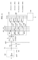
- Fig. 1 is an addition averaging processing circuit diagram using a temporary storage memory of a color imaging apparatus according to a first embodiment of the present invention.
- Fig. 2 is a timing chart of the first embodiment of the present invention.
- Fig. 3 shows a second embodiment of the present invention, also showing the circuit configuration having a CDS circuit and an amplifier.
- Fig. 4 is a timing chart of the second embodiment of the present invention.
- Fig. 5 shows a fourth embodiment of the present invention, also showing an example in which an addition circuit for a plurality of pixel signals and a circuit for plural readings are used in combination.
- Fig. 6 is a timing chart of the fourth embodiment of the present invention.
- Fig. 7 is a configuration diagram in which the addition method after memorization is changed according to a fifth embodiment of the present invention.
- Fig. 8 is a timing chart during all-pixel signal reading.
- Fig. 9 is a timing chart during addition reading.
- Fig. 10 shows the overall configuration diagram of an imaging device of the third embodiment of the present invention.
- Fig. 11 shows the overall configuration diagram of an imaging device of the fourth embodiment of the present invention.
- Fig. 12 is a diagram of an example of the configuration of a common amplifier pixel of a pixel section.
- Fig. 13 shows an imaging apparatus.
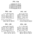
- Fig. 14 shows the color arrangement after a plurality of pixel signal are added.
- Fig. 15 is an arrangement diagram of each color.
- Fig. 14 is an illustration showing the color arrangement and the addition signal for each color after pixel signals are added by the color imaging apparatus according to the embodiments described below.
- Fig. 15A is an arrangement example view for each color before the pixel signals are added.
- color filters G green
- R red
- B blue
- G is arranged in a checkered pattern
- Fig. 15B shows an addition of R i and R j signal, in which the signals of the Rn-th column, the (Rn + 2)th column, and the (Rn + 4)th column of the m-th row, the (m + 2)th row, and the (m + 4)th row are added.
- Fig. 15B shows an addition of R i and R j signal, in which the signals of the Rn-th column, the (Rn + 2)th column, and the (Rn + 4)th column of the m-th row, the (m + 2)th row, and the (m + 4)th row are added.
- Fig. 15B shows an addition of R i and R j signal, in which the signals of the Rn-th column, the (Rn + 2)th column, and the (Rn + 4)th column of the m-th row, the (m + 2)th row,
- FIG. 15C shows an addition of G i and G j+1 signals
- Fig. 15D shows an addition of G i+1 and G j signals
- Fig. 15E shows an addition of B i+1 and B j signals.
- the colors are added in an overlapping manner in terms of space.
- the present invention is applied to an imaging device having five million pixels, the number of pixels becomes approximately a number corresponding to VGA after addition, and a reading of a high-speed image capturing at a high sensitivity becomes possible. Furthermore, if a low resolution is necessary, the number of addition pixels may be increased, for example, as 5 ⁇ 5 or 7 ⁇ 7. Consequently, there is the advantage that a higher sensitivity is obtained. In order to increase the number of addition pixels, the memory of the addition circuit (to be described later) needs only to be increased by an amount corresponding to the number of the addition rows.
- Figs. 1, 3, 5, and 7 are schematic views in which a noise reduction circuit connected to a pixel unit within a memory sensor and a vertical signal line are extracted.
- the pixel unit is a memory sensor in which a plurality of pixel units are arranged in the horizontal and vertical directions, and the noise reduction circuit is connected to the vertical signal line.
- Fig. 1 is a circuit diagram of an addition averaging process of an imaging device for noise N and a signal S' using a temporary storage memory.
- a block 100 surrounded by dotted lines is a pixel unit
- a block 200 is a temporary storage memory, which temporarily stores signals from the pixel unit 100
- a block 300 is a (S-N) difference circuit.
- Pixel noise N reset noise ⁇ KTC, ⁇ Vth, and RN (1/f noise), omitted in the following description
- a signal S' new noise RN' (1/f noise) and a photoelectric conversion signal S are superposed on the reset noise ⁇ Vth, omitted in the following description
- RN of the amplifying transistor becomes 1/ ⁇ 2.
- Reference letter MSF denotes an amplifying transistor which amplifies light charge.
- Reference letter MTX denotes a transfer transistor for transferring light charge that is photoelectrically converted by the photodiode PD to the amplifying transistor MSF.
- Reference letter MSEL denotes a selection transistor for selecting the amplifying transistor MSF.
- Reference letter MRES denotes a transistor for removing the remaining charge in the input section of the amplifying transistor MSF.
- reference letter Vn denotes a vertical signal line connected to the amplifying transistor MSF
- reference letter MRV denotes a transistor for the electrical current source of the amplifying transistor MSF
- Reference letters CT1 and CT2 each denote a capacitor for temporarily storing pixel noise.
- Reference letters CT3 and CT4 each denote a capacitor for temporarily storing a pixel signal.
- Input transistors MT1 to MT4 to capacitors CT1 to CT4, respectively, are each a transfer transistor for controlling the transfer of noise and signals from the amplifying transistor MSF.
- Output transistors MTO1 to MTO4 from capacitors CT1 to CT4, respectively, are each a transistor for transferring noise and a signal to horizontal signal lines L1 and L2.
- the transfer of the transfer transistor is controlled in accordance with the pulses ⁇ T1 to ⁇ T4, and ⁇ hn.
- ⁇ hn is a pulse from the horizontal scanning circuit (not shown in the figure).
- Reference letters Mh1 and Mh2 each denote a reset transistor for resetting a remaining signal of the horizontal signal line.
- Reference numeral 300-1 denotes a differential amplifier for noise N and the signal S'.
- Fig. 2 shows a timing chart of the main operation.
- the remaining charge of the input gate section of the amplifying transistor is reset in the t1 period of the pulse ⁇ RES.
- the pixel noise N1 ( ⁇ KTC + ⁇ Vth + RN1) is stored in the capacitor CT1.
- the pixel noise N2 ( ⁇ KTC + ⁇ Vth + RN2) is stored in the capacitor CT2.
- the light charge S that is photoelectrically converted by the photodiode PD is transferred to the input section of the amplifying transistor MSF.
- the signal S' (S + ⁇ KTC + ⁇ Vth + RN3) is stored in the capacitor CT3
- the signal S' (S + ⁇ KTC + ⁇ Vth + RN4) is stored in the capacitor CT4. This follows that each of the noise and the signal are stored two times (t2 and t3, t5 and t6) from the amplifying transistor MSF. These operations are performed for each of a plurality of the pixel rows which are connected in the horizontal direction in the actual area sensor.
- the noise and the signal of the memory are simultaneously transferred to the horizontal signal lines L1 and L2 in accordance with the pulse ⁇ h (n) from the horizontal scanning circuit, and become the added and averaged noise ( ⁇ KTC + ⁇ Vth + RN'/ ⁇ 2) and signal (S + ⁇ KTC + ⁇ Vth + RN"/ ⁇ 2). Then, the fixed pattern noise is removed by the differential process by the differential amplifier 300-1, and a signal Vout (S + RN) is output. ⁇ hreset is used to reset the remaining charge of the horizontal signal line so as to be in preparation for the next transfer of the noise and the signal.
- FIG. 3 A second embodiment of the present invention is shown in Fig. 3.
- a CDS circuit for removing fixed pattern noise of the amplifying transistor and an amplifying circuit 5 are provided between the pixel unit block 100 and the temporary storage memory block 200.
- the CDS circuit enables ⁇ KTC noise of the clamping capacitor and noise of the amplifying transistor ( ⁇ KTC + ⁇ Vth) to be removed.
- the amplifier 5 makes it possible to obtain a signal level in such a degree that the noise of the circuit at the subsequent stage can be ignored. It is also possible for this amplifier 5 to switch the gain of the imaging device. During low illumination time, this is convenient for avoiding the influence of the noise of the subsequent stage circuit.
- a clamping capacitor Ccl for CDS is connected to a vertical signal line Vn, and a clamping transistor Mcl is connected to a desired reference power supply at the end of the clamping capacitor.
- the variation components of the amplifying transistor that is, RN noise and the variation voltage for light charge, are input to the amplifier.
- the noise and the signal are amplified, the offset voltage of the amplifier is superposed thereon, and the result is stored in the temporary storage memory 200.
- Fig. 4 shows an operation timing chart of the second embodiment of the present invention.
- the input end of the clamping capacitor is clamped to the noise electrical potential of the amplifying transistor, and the end thereof is clamped to the reference electrical potential.
- the offset voltage and the noise of the amplifier are stored in the memory in accordance with the pulse ⁇ T1.
- the offset voltage and the noise of the amplifier are stored in the memory in accordance with the pulse ⁇ T2.
- the photoelectric conversion signal S, and the offset voltage and the noise of the amplifier are stored in the memory in the periods t5 and t6.
- the noise and the signal of the memory are simultaneously transferred to the horizontal signal lines L1 and L2 in accordance with the pulse ⁇ h (n) from the horizontal scanning circuit and become the noise ( ⁇ Voffset + RN' ⁇ 2) and the signal (S + ⁇ Voffset + RN"/ ⁇ 2), which are added and averaged.
- the offset noise ( ⁇ Voffset) of the amplifier is removed by the differential process of the differential amplifier 300-1, and a signal Vout (S + RN) is output.
- the noise contained in the signal Vout is the same in the description.
- Fig. 10 shows a schematic view of the overall configuration of an imaging apparatus of a third embodiment of the present invention.
- a plurality of pixel units are formed in the horizontal and vertical directions in an image-capturing area 35.
- a microlense for improving the collection of light, a color filter for colorization, and the like, are formed in the pixel unit (not shown in the figure).
- the pixel of each pixel row within the image-capturing area 35 is controlled by the vertical scanning circuit 10.
- Fig. 10 within the image-capturing area 35, only the vertical signal lines V1 to Vn are shown schematically.
- the vertical signal lines are connected to a corresponding CDS and amplifying circuits 20-1 and 20-2 in the odd-numbered columns and the even-numbered columns, respectively, and the output signals are temporarily stored in the memories 30-1 and 30-2. Then, the noise and the signal of the memories are guided to the differential amplifiers 50-1 and 50-2 in accordance with the control pulse of the horizontal scanning circuits 40-1 and 40-2, and the noise is reduced.
- the CDS amplifying circuits 20-1, 20-2 correspond to CcL and McL in Fig. 3. Furthermore, the CDS amplifying circuits 20-1, 20-2 correspond to the amplifying circuit 5 in Fig. 3.
- the memories 30-1, 30-2 correspond to the temporary storage memory 200 in Fig. 3.
- the differential amplifiers 50-1 and 50-2 correspond to the difference circuit 300 in Fig. 3.
- composition and operation of the third embodiment are the same as those of the second embodiment (shown in Fig. 3) except for reading to the bottom in the even-numbered columns and reading to the bottom in an odd-numbered columns in the third embodiment (Fig. 10).
- a fourth embodiment explains the composition and operation of the imaging device in a case of 3 x 3 pixels.
- Fig. 5 is a circuit configuration in which addition averaging of the pixel signals of three pixels and three readings of noise and a signal are used in combination.
- Fig. 6 is a driving timing chart of the fourth embodiment of the present invention.
- Figs. 15B - 15E addition averaging of a plurality of 3 x 3 pixels is performed.
- terminals after the CDS of pixel units 100-1 to 100-3 of the pixel row m are connected by transistors Mco1 and Mco2, and during addition, the conduction of this transistor is controlled in accordance with a pulse ⁇ add.
- the noise and the signal after the CDS from the three pixel units are added and averaged in accordance with pulses ( ⁇ T1 to ⁇ T6, and ⁇ TX) in the period t1, and are stored in the memories CT0 to CT5 after passing through an amplifier 5-1.
- the noise and the signal are read three times and are stored in a memory 200'-1.
- addition averaging of the noise and the signals of the three pixels, and plural readings thereof are performed in accordance with pulses ( ⁇ T1' to ⁇ T6' , and ⁇ TX') and are stored in a memory 200'-2.
- addition averaging of the noise and the signal of three pixels, and plural readings thereof are performed in accordance with pulses ( ⁇ T1" to ⁇ T6", and ⁇ TX") and are stored in a memory 200-3'.
- the noise RN can be reduced to 1/(3 ⁇ 3).
- the noise RN becomes ⁇ 2/(3 ⁇ 3).
- the noise RN is reduced to 1/(3 ⁇ 3), and thus, the sensitivity is improved by 1 / ⁇ 2 times (i.e., by about 70%).
- Fig. 11 is a circuit block diagram of an imaging device of the fourth embodiment of the present invention.
- the major difference between Fig. 11 and Fig. 10 is that in Fig. 11 an addition circuit(Mcol, Mco2) 15-1 is additionally provided, and an amplifying circuit 25-2 is formed at the subsequent stage.
- Mco2 addition circuit
- the addition after the storing capacitor CT (CT0 - CT5) of the memory 200 is performed at a stage prior to transferring noise and a signal to the horizontal signal line (Fig. 7) .
- CT0 - CT5 the storing capacitor CT
- the composition and operation other than the above is the same as a case of the fourth embodiment.
- the number of transistors connected to the horizontal signal line is reduced, the parasitic capacitance is reduced, and the transfer efficiency from the memory to the horizontal signal line by capacitance division can be improved.
- Fig. 8 is a timing chart in the case of all-pixel reading.
- Fig. 9 is a timing chart in the case of addition reading.
- the addition of plural pixel signals is turned on in accordance with an addition pulse ⁇ add, and horizontal transfer pulses ⁇ hn, ⁇ hn', and ⁇ hn" are controlled independently.
- ⁇ hn, ⁇ hn', and ⁇ hn" are controlled in accordance with a common pulse.
- the configuration in which one amplifying transistor is formed with respect to one photodiode is described.
- a common amplifier pixel configuration is shown in Fig. 12. This is an example in which two photodiodes are formed with respect to one amplifying transistor. If a plurality of photodiodes are arranged with respect to one amplifier, the area of the amplifying transistor with respect to one photodiode becomes smaller, with the result that there is the advantage that the aperture ratio of the photodiode is improved.
- Fig. 13 shows a schematic view of an imaging apparatus using the above-described imaging device.
- subject light which enters through an optical system 71 is formed into an image on a sensor 72.
- the light information is converted into an electrical signal by the pixels arranged in the sensor.
- the electrical signal is subjected to a signal conversion process by a signal processing circuit 73 by using a predetermined method.
- the processed signal is recorded into or transmitted into an information recording device by a recording system/communication system 74.
- the recorded or transferred signal is played back or displayed in the playback system or in the display system.
- the sensor 72 and the signal processing circuit 73 are controlled by a timing control circuit 75.
- the timing control circuit 75, the recording system/communication system 74, and the playback system/display system 77 are controlled by a system control circuit 76.
- the timing control circuit 75 makes a selection of an all-pixel reading mode or an addition reading mode (as described in the fourth - fifth embodiments).
- the imaging device in the first embodiment through the fifth embodiment is driven by timing control circuit 75.
- the imaging apparatus in the high-precision image capturing, it is possible to perform all-pixel reading in order to achieve a higher sensitivity, and in the low resolution image-capturing, ultra-high sensitivity, high-speed reading, and high image quality are made possible.
- 1/f noise of the amplifying transistor can be reduced by reading plural times the noise and the signal from the pixel and by adding and averaging them. Since the addition of pixel signals and plural readings are used in combination, 1/f noise can be further reduced, and higher sensitivity is achieved. Since the centers of gravities of the spatial sampling of each color signal are made to match each other, moire fringing can be reduced. As a result of adding the pixel signals, the sensitivity can be improved, and high-speed reading and low power consumption become possible. Since the addition circuit can be formed small, imaging devices can be provided at a low price.
Landscapes
- Engineering & Computer Science (AREA)
- Multimedia (AREA)
- Signal Processing (AREA)
- Transforming Light Signals Into Electric Signals (AREA)
- Solid State Image Pick-Up Elements (AREA)
- Color Television Image Signal Generators (AREA)
Applications Claiming Priority (2)
| Application Number | Priority Date | Filing Date | Title |
|---|---|---|---|
| JP2003430427 | 2003-12-25 | ||
| JP2003430427 | 2003-12-25 |
Publications (2)
| Publication Number | Publication Date |
|---|---|
| EP1549050A2 true EP1549050A2 (de) | 2005-06-29 |
| EP1549050A3 EP1549050A3 (de) | 2006-05-17 |
Family
ID=34545024
Family Applications (1)
| Application Number | Title | Priority Date | Filing Date |
|---|---|---|---|
| EP04258182A Withdrawn EP1549050A3 (de) | 2003-12-25 | 2004-12-23 | Bildaufnahmevorrichtung zur Verarbeitung von Rausch- und fotoelektrisches Umwandlungssignal |
Country Status (3)
| Country | Link |
|---|---|
| US (2) | US7692704B2 (de) |
| EP (1) | EP1549050A3 (de) |
| CN (2) | CN1638445A (de) |
Cited By (6)
| Publication number | Priority date | Publication date | Assignee | Title |
|---|---|---|---|---|
| WO2007135158A1 (en) * | 2006-05-23 | 2007-11-29 | Thomson Licensing | Image sensor circuit |
| WO2009099116A1 (en) * | 2008-02-06 | 2009-08-13 | Canon Kabushiki Kaisha | Driving method of solid-state imaging apparatus, solid-state imaging apparatus, and imaging system |
| EP2271077A1 (de) * | 2009-06-30 | 2011-01-05 | Canon Kabushiki Kaisha | Verfahren und Vorrichtung zur Rauschunterdrückung in Bildsensor-Geräten |
| GB2479594A (en) * | 2010-04-16 | 2011-10-19 | St Microelectronics | A sample and hold circuit with internal averaging of samples |
| EP2334055A3 (de) * | 2009-12-07 | 2015-12-09 | Canon Kabushiki Kaisha | Photoelektrische Umwandlungsvorrichtung |
| FR3023653A1 (fr) * | 2014-07-09 | 2016-01-15 | Commissariat Energie Atomique | Capteur d'images cmos a echantillonnage multiple correle |
Families Citing this family (15)
| Publication number | Priority date | Publication date | Assignee | Title |
|---|---|---|---|---|
| JP4154268B2 (ja) * | 2003-03-27 | 2008-09-24 | キヤノン株式会社 | 撮像装置 |
| JP2005286115A (ja) * | 2004-03-30 | 2005-10-13 | Fuji Film Microdevices Co Ltd | 光電変換膜積層型固体撮像装置及びその駆動方法並びにデジタルカメラ |
| JP4290066B2 (ja) * | 2004-05-20 | 2009-07-01 | キヤノン株式会社 | 固体撮像装置および撮像システム |
| JP2008182314A (ja) * | 2007-01-23 | 2008-08-07 | Matsushita Electric Ind Co Ltd | 位相調整装置およびその関連技術 |
| JP5142696B2 (ja) * | 2007-12-20 | 2013-02-13 | キヤノン株式会社 | 光電変換装置、及び光電変換装置を用いた撮像システム |
| JP5341636B2 (ja) * | 2009-06-24 | 2013-11-13 | キヤノン株式会社 | 撮像装置の読み出し方法、及び撮像装置 |
| JP5634194B2 (ja) * | 2010-09-28 | 2014-12-03 | キヤノン株式会社 | 放射線撮像装置及びその制御方法 |
| US9854138B2 (en) * | 2012-09-20 | 2017-12-26 | Gyrus Acmi, Inc. | Fixed pattern noise reduction |
| JP6272046B2 (ja) * | 2014-01-22 | 2018-01-31 | キヤノン株式会社 | 放射線撮像装置、その制御方法、及び放射線検査装置 |
| CN103873785B (zh) * | 2014-03-26 | 2017-08-11 | 中国科学院光电技术研究所 | 一种低噪声电荷耦合器件前端模拟视频信号预处理装置 |
| CN110771155B (zh) | 2017-05-10 | 2021-11-16 | 普里露尼库斯新加坡私人有限公司 | 固态摄像装置、固态摄像装置的驱动方法、以及电子设备 |
| JP7245001B2 (ja) * | 2018-05-29 | 2023-03-23 | キヤノン株式会社 | 放射線撮像装置および撮像システム |
| JP6567792B1 (ja) * | 2019-04-04 | 2019-08-28 | キヤノン電子管デバイス株式会社 | 放射線検出器 |
| US11095842B2 (en) * | 2019-07-26 | 2021-08-17 | Omnivision Technologies, Inc. | Image sensor with electronic global shutter and differential sensing using reset-sampling capacitor shared among multiple image storage capacitors |
| US20230178571A1 (en) * | 2021-12-06 | 2023-06-08 | ams Sensors USA Inc. | Pixel arrangement, pixel matrix, image sensor and method of operating a pixel arrangement |
Family Cites Families (18)
| Publication number | Priority date | Publication date | Assignee | Title |
|---|---|---|---|---|
| US4262258A (en) * | 1979-02-06 | 1981-04-14 | Nasa | CCD Correlated quadruple sampling processor |
| JPS6386976A (ja) | 1986-09-30 | 1988-04-18 | Nec Corp | 雑音除去回路 |
| US4902886A (en) * | 1989-01-23 | 1990-02-20 | Hewlett-Packard Company | Noise reduction for photodiode arrays |
| US5943094A (en) * | 1991-09-04 | 1999-08-24 | Canon Kabushiki Kaisha | Image pickup device with noise data generation |
| US5371470A (en) * | 1993-03-04 | 1994-12-06 | Photometrics, Ltd. | Transverse filter circuit |
| JPH09247689A (ja) * | 1996-03-11 | 1997-09-19 | Olympus Optical Co Ltd | カラー撮像装置 |
| KR970072990A (ko) * | 1996-04-10 | 1997-11-07 | 이데이 노부유끼 | 고체 화상 장치 |
| JPH10257389A (ja) | 1997-03-11 | 1998-09-25 | Toshiba Corp | 増幅型固体撮像装置及びその動作方法 |
| US6037577A (en) * | 1997-03-11 | 2000-03-14 | Kabushiki Kaisha Toshiba | Amplifying solid-state image pickup device and operating method of the same |
| US6040570A (en) * | 1998-05-29 | 2000-03-21 | Sarnoff Corporation | Extended dynamic range image sensor system |
| US6765613B1 (en) * | 1998-07-22 | 2004-07-20 | Micron Technology, Inc. | Low light sensor signal to noise improvement |
| JP3501694B2 (ja) | 1999-07-21 | 2004-03-02 | キヤノン株式会社 | 撮像装置及びそれを用いた撮像システム |
| US6992714B1 (en) * | 1999-05-31 | 2006-01-31 | Canon Kabushiki Kaisha | Image pickup apparatus having plural pixels arranged two-dimensionally, and selective addition of different pixel color signals to control spatial color arrangement |
| US7324144B1 (en) * | 1999-10-05 | 2008-01-29 | Canon Kabushiki Kaisha | Solid image pickup device, image pickup system and method of driving solid image pickup device |
| JP3894534B2 (ja) * | 2001-05-16 | 2007-03-22 | キヤノン株式会社 | 撮像装置および放射線撮像装置 |
| JP2003037780A (ja) | 2001-07-24 | 2003-02-07 | Fuji Photo Film Co Ltd | 画像データ取得方法および装置 |
| JP2003204487A (ja) | 2002-01-09 | 2003-07-18 | Sony Corp | 信号処理回路 |
| JP3937870B2 (ja) * | 2002-02-27 | 2007-06-27 | 日本ビクター株式会社 | 撮像装置 |
-
2004
- 2004-12-17 US US11/015,240 patent/US7692704B2/en not_active Expired - Fee Related
- 2004-12-23 EP EP04258182A patent/EP1549050A3/de not_active Withdrawn
- 2004-12-24 CN CNA2004100114884A patent/CN1638445A/zh active Pending
- 2004-12-24 CN CN2009102264249A patent/CN101707667B/zh not_active Expired - Fee Related
-
2010
- 2010-02-18 US US12/708,262 patent/US8384804B2/en not_active Expired - Fee Related
Non-Patent Citations (1)
| Title |
|---|
| None * |
Cited By (11)
| Publication number | Priority date | Publication date | Assignee | Title |
|---|---|---|---|---|
| WO2007135158A1 (en) * | 2006-05-23 | 2007-11-29 | Thomson Licensing | Image sensor circuit |
| US8102442B2 (en) | 2006-05-23 | 2012-01-24 | Thomson Licensing | Image sensor circuit |
| WO2009099116A1 (en) * | 2008-02-06 | 2009-08-13 | Canon Kabushiki Kaisha | Driving method of solid-state imaging apparatus, solid-state imaging apparatus, and imaging system |
| US8305473B2 (en) | 2008-02-06 | 2012-11-06 | Canon Kabushiki Kaisha | Driving method of solid-state imaging apparatus, solid-state imaging apparatus, and imaging system |
| EP2271077A1 (de) * | 2009-06-30 | 2011-01-05 | Canon Kabushiki Kaisha | Verfahren und Vorrichtung zur Rauschunterdrückung in Bildsensor-Geräten |
| US8928779B2 (en) | 2009-06-30 | 2015-01-06 | Canon Kabushiki Kaisha | Image pickup apparatus, image pickup system, and control method thereof |
| EP2334055A3 (de) * | 2009-12-07 | 2015-12-09 | Canon Kabushiki Kaisha | Photoelektrische Umwandlungsvorrichtung |
| GB2479594A (en) * | 2010-04-16 | 2011-10-19 | St Microelectronics | A sample and hold circuit with internal averaging of samples |
| US8698882B2 (en) | 2010-04-16 | 2014-04-15 | Stmicroelectronics (Research & Development) Limited | Sample and hold circuit |
| FR3023653A1 (fr) * | 2014-07-09 | 2016-01-15 | Commissariat Energie Atomique | Capteur d'images cmos a echantillonnage multiple correle |
| US9497400B2 (en) | 2014-07-09 | 2016-11-15 | Commissariat a lénergie atomique et aux energies alternatives | Correlated multiple sampling CMOS image sensor |
Also Published As
| Publication number | Publication date |
|---|---|
| US20050146617A1 (en) | 2005-07-07 |
| US20100141790A1 (en) | 2010-06-10 |
| CN1638445A (zh) | 2005-07-13 |
| CN101707667A (zh) | 2010-05-12 |
| EP1549050A3 (de) | 2006-05-17 |
| US7692704B2 (en) | 2010-04-06 |
| US8384804B2 (en) | 2013-02-26 |
| CN101707667B (zh) | 2012-08-08 |
Similar Documents
| Publication | Publication Date | Title |
|---|---|---|
| US8384804B2 (en) | Imaging apparatus for processing noise signal and photoelectric conversion signal | |
| US9214491B2 (en) | Solid-state imaging apparatus for causing an FD capacitor value to be variable without increasing a number of elements | |
| CN1946136B (zh) | 一种成像设备的驱动方法 | |
| US7978240B2 (en) | Enhancing image quality imaging unit and image sensor | |
| US9438839B2 (en) | Solid state imaging apparatus and imaging system using the same | |
| US20060262209A1 (en) | Image sensing device and control method therefor | |
| US8754971B2 (en) | Image sensing apparatus and image capturing system | |
| US20150021460A1 (en) | Solid state imaging device and imaging apparatus | |
| US10425605B2 (en) | Image sensor and image capturing apparatus | |
| RU2378791C2 (ru) | Устройство для восприятия изображений и система для захвата изображений | |
| US20150288903A1 (en) | Solid-state image sensor, image capturing apparatus and control method thereof, and storage medium | |
| JP4677228B2 (ja) | 撮像装置 | |
| JP2025147036A (ja) | 撮像素子及び撮像装置 | |
| KR100823376B1 (ko) | 촬상장치 및 촬상시스템 | |
| JP2008172704A (ja) | 固体撮像装置及びその駆動方法 | |
| JPH04154284A (ja) | 固体撮像装置の駆動方法 | |
| US8054364B2 (en) | Image apparatus and drive control method for image pickup device with horizontal addition of pixel data | |
| JP5511205B2 (ja) | 撮像装置及び撮像方法 | |
| JP4228755B2 (ja) | 固体撮像素子および固体撮像素子の駆動方法 | |
| JP2018088721A (ja) | 固体撮像素子、撮像装置及びその制御方法、プログラム、記憶媒体 | |
| KR20160097937A (ko) | 이미지 센싱 장치 | |
| JP2008118371A (ja) | 撮像素子 |
Legal Events
| Date | Code | Title | Description |
|---|---|---|---|
| PUAI | Public reference made under article 153(3) epc to a published international application that has entered the european phase |
Free format text: ORIGINAL CODE: 0009012 |
|
| AK | Designated contracting states |
Kind code of ref document: A2 Designated state(s): AT BE BG CH CY CZ DE DK EE ES FI FR GB GR HU IE IS IT LI LT LU MC NL PL PT RO SE SI SK TR |
|
| AX | Request for extension of the european patent |
Extension state: AL BA HR LV MK YU |
|
| PUAL | Search report despatched |
Free format text: ORIGINAL CODE: 0009013 |
|
| AK | Designated contracting states |
Kind code of ref document: A3 Designated state(s): AT BE BG CH CY CZ DE DK EE ES FI FR GB GR HU IE IS IT LI LT LU MC NL PL PT RO SE SI SK TR |
|
| AX | Request for extension of the european patent |
Extension state: AL BA HR LV MK YU |
|
| 17P | Request for examination filed |
Effective date: 20061117 |
|
| AKX | Designation fees paid |
Designated state(s): DE FR |
|
| 17Q | First examination report despatched |
Effective date: 20070126 |
|
| STAA | Information on the status of an ep patent application or granted ep patent |
Free format text: STATUS: THE APPLICATION HAS BEEN WITHDRAWN |
|
| 18W | Application withdrawn |
Effective date: 20160202 |