EP1548933A1 - Verfahren zum Verhindern abrupter Spannungsänderungen am Ausgang eines Verstärkerpaars und Regelschaltung für ein selbstkonfigurierendes Verstärkerpaar in einer Brückenkonfiguration - Google Patents
Verfahren zum Verhindern abrupter Spannungsänderungen am Ausgang eines Verstärkerpaars und Regelschaltung für ein selbstkonfigurierendes Verstärkerpaar in einer Brückenkonfiguration Download PDFInfo
- Publication number
- EP1548933A1 EP1548933A1 EP03425816A EP03425816A EP1548933A1 EP 1548933 A1 EP1548933 A1 EP 1548933A1 EP 03425816 A EP03425816 A EP 03425816A EP 03425816 A EP03425816 A EP 03425816A EP 1548933 A1 EP1548933 A1 EP 1548933A1
- Authority
- EP
- European Patent Office
- Prior art keywords
- opa
- amplifiers
- pair
- common mode
- amplifier
- Prior art date
- Legal status (The legal status is an assumption and is not a legal conclusion. Google has not performed a legal analysis and makes no representation as to the accuracy of the status listed.)
- Granted
Links
- 238000000034 method Methods 0.000 title description 9
- 239000003990 capacitor Substances 0.000 description 3
- 230000005236 sound signal Effects 0.000 description 3
- 230000002596 correlated effect Effects 0.000 description 2
- 238000010586 diagram Methods 0.000 description 2
- 229920006395 saturated elastomer Polymers 0.000 description 2
- 230000001934 delay Effects 0.000 description 1
- 230000009977 dual effect Effects 0.000 description 1
- 238000009434 installation Methods 0.000 description 1
- 230000003287 optical effect Effects 0.000 description 1
- 238000005070 sampling Methods 0.000 description 1
Images


Classifications
-
- H—ELECTRICITY
- H03—ELECTRONIC CIRCUITRY
- H03F—AMPLIFIERS
- H03F3/00—Amplifiers with only discharge tubes or only semiconductor devices as amplifying elements
- H03F3/45—Differential amplifiers
- H03F3/45071—Differential amplifiers with semiconductor devices only
- H03F3/45076—Differential amplifiers with semiconductor devices only characterised by the way of implementation of the active amplifying circuit in the differential amplifier
- H03F3/45475—Differential amplifiers with semiconductor devices only characterised by the way of implementation of the active amplifying circuit in the differential amplifier using IC blocks as the active amplifying circuit
-
- H—ELECTRICITY
- H03—ELECTRONIC CIRCUITRY
- H03F—AMPLIFIERS
- H03F1/00—Details of amplifiers with only discharge tubes, only semiconductor devices or only unspecified devices as amplifying elements
- H03F1/02—Modifications of amplifiers to raise the efficiency, e.g. gliding Class A stages, use of an auxiliary oscillation
- H03F1/0205—Modifications of amplifiers to raise the efficiency, e.g. gliding Class A stages, use of an auxiliary oscillation in transistor amplifiers
- H03F1/0277—Selecting one or more amplifiers from a plurality of amplifiers
-
- H—ELECTRICITY
- H03—ELECTRONIC CIRCUITRY
- H03F—AMPLIFIERS
- H03F1/00—Details of amplifiers with only discharge tubes, only semiconductor devices or only unspecified devices as amplifying elements
- H03F1/32—Modifications of amplifiers to reduce non-linear distortion
-
- H—ELECTRICITY
- H03—ELECTRONIC CIRCUITRY
- H03F—AMPLIFIERS
- H03F3/00—Amplifiers with only discharge tubes or only semiconductor devices as amplifying elements
- H03F3/30—Single-ended push-pull [SEPP] amplifiers; Phase-splitters therefor
- H03F3/3081—Duplicated single-ended push-pull arrangements, i.e. bridge circuits
-
- H—ELECTRICITY
- H03—ELECTRONIC CIRCUITRY
- H03F—AMPLIFIERS
- H03F3/00—Amplifiers with only discharge tubes or only semiconductor devices as amplifying elements
- H03F3/68—Combinations of amplifiers, e.g. multi-channel amplifiers for stereophonics
-
- H—ELECTRICITY
- H03—ELECTRONIC CIRCUITRY
- H03F—AMPLIFIERS
- H03F2200/00—Indexing scheme relating to amplifiers
- H03F2200/03—Indexing scheme relating to amplifiers the amplifier being designed for audio applications
-
- H—ELECTRICITY
- H03—ELECTRONIC CIRCUITRY
- H03F—AMPLIFIERS
- H03F2200/00—Indexing scheme relating to amplifiers
- H03F2200/114—Indexing scheme relating to amplifiers the amplifier comprising means for electro-magnetic interference [EMI] protection
-
- H—ELECTRICITY
- H03—ELECTRONIC CIRCUITRY
- H03F—AMPLIFIERS
- H03F2203/00—Indexing scheme relating to amplifiers with only discharge tubes or only semiconductor devices as amplifying elements covered by H03F3/00
- H03F2203/45—Indexing scheme relating to differential amplifiers
- H03F2203/45138—Two or more differential amplifiers in IC-block form are combined, e.g. measuring amplifiers
Definitions
- the present invention relates in general to amplifiers with a reduced power consumption specially for car radio and HI-FI audio applications and in particular to a method of preventing abrupt voltage changes at the outputs of a pair of amplifiers and a common mode control circuit implementing this method.
- HI-FI audio systems and similar apparatuses that are intrinsically compact because of stringent installation requirements, as well as in portable apparatuses, power dissipation in final power stages, often quadrupled in order to drive a pair of loudspeakers (front and rear) for each stereo channel, may create heat balance problems.
- D-type switching amplifiers are highly efficient and are considered the most appropriate type for these applications.
- class AB power amplifiers are less efficient than switching amplifiers and a common technique for reducing power consumption of class AB amplifiers single-ended mode or in bridge configuration depending on the level of the processed signal.
- class AB power amplifiers are less efficient than switching amplifiers and a common technique for reducing power consumption of class AB amplifiers consists in configuring them in single-ended instead of in bridge configuration whenever it is possible to do so. In fact, these amplifiers dissipate more power in bridge configuration than in single-ended configuration as long as the level of the output signal remains smaller than the positive supply voltage. Unfortunately, it is not possible to use single-ended class AB amplifiers if the output surpasses this voltage because the output signal would be severely distorted by clipping.
- the patent US 5,194,821 discloses a bridge amplifier using positive and negative supply voltages, that may function in single-ended or in differential or bridge output configuration, depending on the level of the output signal. Substantially, a comparator changes the output circuital configuration of the amplifier from a bridge configuration to a single-ended configuration or vice versa by closing or opening configuring switches, when the output signal becomes smaller than or greater than a certain threshold voltage.
- the switching from a single-ended to a bridge output configuration and vice versa may cause distortions and EMI disturbances in view of the fact that, when functioning with relatively low signal level, one of the operational amplifiers of the bridge output structure is configured to work as a buffer outputting a constant reference voltage that usually is equal to half the supply voltage and whenever it must switch to function as a second operational amplifier for driving the load in a bridge mode following an increase of the signal level, this operational amplifier must rapidly assume a different output voltage, that is its output voltage undergoes a step variation.
- the independent equalization setting on the various channels cause different delays of propagation of signals through the channels, that thus become substantially uncorrelated.
- Figure 3 depicts sample diagrams of differential pairs of signals OUT_F+, OUT_F-and OUT_R+, OUT_R- output by the left OPA+F, OPA-F and right OPA+R, OPA-R channels.
- the signals are referred to a fixed voltage, which is generally half the supply voltage VCC and are substantially uncorrelated.
- the common mode voltages of the left and right channels, respectively, are sampled when the amplifier switches to bridge configuration and are held as long as the amplifier switches to single-ended configuration.
- the input signals are substantially uncorrelated, it is very likely that the output signals undergo step variations when the amplifier switches from bridge to single-end configuration (instants t2 and t4).
- both the amplifier OPA+R that must switch in bridge configuration and the amplifier OPA-F that must be disconnected may output signals with an amplitude far larger than the fixed voltage VCC/2. Therefore, when the switch SW_C turns on, the outputs of both channels OPA+R and OPA-F must quickly reach the fixed voltage Vcc/2, generating a step variation that produces EMI and distortions.
- This step variation propagates also to the other channels OPA-R and OPA+F, through the feedback lines. Even the power switch SW_C may turn on when it withstands is a high differential voltage, thus generating a cross-conduction current that is likely to cause the intervention of the protection circuit from short-circuits.
- a multi-channel power amplifier capable of sensibly reducing EMI and distortions is disclosed in the European patent application No. 03425357.5 in the name of the same Applicant. Its design ensures that one of the two operational amplifiers of the output bridge structure of each channel be kept at the design reference voltage (typically to half the supply voltage) for as long as the other operational amplifier of the output bridge structure does not begin to saturate by connecting in common the gate nodes of the P-type MOS transistors and the gate nodes of the N-type MOS transistors of the output half bridge stages of all the operational amplifiers of the output bridge pairs of all the channels that are eventually configured to function as voltage reference buffer, when configuring the multi channel amplifier to function in a single-ended configuration.
- the design reference voltage typically to half the supply voltage
- the switches that connect in common the gate nodes of the power transistors of the same type are controlled in phase with the switches that configure the multi channel amplifier to function in a single-ended configuration, referred to a constant reference voltage.
- a method of preventing abrupt voltage changes at the outputs of a pair of amplifiers and a common mode control circuit of a pair of amplifiers that solve the above mentioned problems that affect multi-channel amplifiers in presence of uncorrelated audio signals to be amplified has been found.
- this result is attained by properly generating for each amplifier a reference potential as a saturated replica of the respective differential input signal of the amplifier that saturates when the amplifier switches to a bridge configuration.
- This method is implemented in a common mode control circuit for a pair of amplifiers self-configuring in a bridge configuration for driving a first load and in a single-ended mode of operation of one of the amplifiers for driving the first load, in function of the level of a differential input signal, comprising
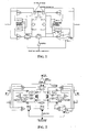
- FIG. 4 A detailed diagram of a bridge amplifier including a common mode control circuit realized to this invention is depicted in Figure 4, wherein R1, ... R12 are resistors and the block PSW_LOGIC contains the logic circuitry that controls the power switch PSW.
- this bridge amplifier is similar to that of the prior art amplifier of Figure 2, but the storage capacitors C1 and C2 are not referred to ground potential as in the prior art circuit, on the contrary they are referred to voltages V CM _F and V CM _R, respectively, that are a saturated replica of the respective input signal.
- these voltages V CM _F and V CM _R are purposely generated by the differential/single-ended converters CV_F and CV_R, respectively, and range within the same voltage levels V REF + and V REF - that define the comparison window of the input differential signals within which the amplifier is in single-end configuration.
- V REF + or V REF -
- V REF - the respective reference voltage V CM _F or V CM _R
- FIG. 5 illustrates the waveforms of the output signals of the left and right channels.
- the common mode feedback amplifiers Gm1, Gm2 sense the difference between the signals OUT_F+, OUT_R- (suitably scaled by the voltage dividers R9, R10 and R11, R12) and the common mode voltages of the respective channels stored on the sampling capacitors C1, C2.
- the saturation values of the reference voltages V CM _F and V CM _R are the levels V REF +, V REF - that define the comparison window for the input differential signal
- the common mode voltages of the output signals are half the voltages OUT_F+ and OUT_R- when the amplifier is switched in single-end configuration, thus the other signals OUT_F- and OUT_R+ are null and there is no step variation of the output signals.
- a bridge amplifier including a common mode control circuit of this invention prevents step variations of the output signals when switching from bridge to single-end configuration, ensuring lower distortion and EMI figures than prior art amplifiers.
- the circuit of this invention is thus particularly suited for realizing audio amplifiers for Dolby@ surround and home theatre systems, which are characterized by substantially uncorrelated input audio signals to be amplified.
Landscapes
- Engineering & Computer Science (AREA)
- Power Engineering (AREA)
- Physics & Mathematics (AREA)
- Nonlinear Science (AREA)
- Amplifiers (AREA)
Priority Applications (3)
| Application Number | Priority Date | Filing Date | Title |
|---|---|---|---|
| DE60317806T DE60317806T2 (de) | 2003-12-23 | 2003-12-23 | Verfahren zum Verhindern abrupter Spannungsänderungen am Ausgang eines Verstärkerpaars und Regelschaltung für ein selbstkonfigurierendes Verstärkerpaar in einer Brückenkonfiguration |
| EP03425816A EP1548933B1 (de) | 2003-12-23 | 2003-12-23 | Verfahren zum Verhindern abrupter Spannungsänderungen am Ausgang eines Verstärkerpaars und Regelschaltung für ein selbstkonfigurierendes Verstärkerpaar in einer Brückenkonfiguration |
| US11/022,020 US7230482B2 (en) | 2003-12-23 | 2004-12-23 | Method of preventing abrupt voltage changes at the outputs of a pair of amplifiers and control circuit for a pair of amplifiers self-configuring in a bridge configuration |
Applications Claiming Priority (1)
| Application Number | Priority Date | Filing Date | Title |
|---|---|---|---|
| EP03425816A EP1548933B1 (de) | 2003-12-23 | 2003-12-23 | Verfahren zum Verhindern abrupter Spannungsänderungen am Ausgang eines Verstärkerpaars und Regelschaltung für ein selbstkonfigurierendes Verstärkerpaar in einer Brückenkonfiguration |
Publications (2)
| Publication Number | Publication Date |
|---|---|
| EP1548933A1 true EP1548933A1 (de) | 2005-06-29 |
| EP1548933B1 EP1548933B1 (de) | 2007-11-28 |
Family
ID=34530871
Family Applications (1)
| Application Number | Title | Priority Date | Filing Date |
|---|---|---|---|
| EP03425816A Expired - Lifetime EP1548933B1 (de) | 2003-12-23 | 2003-12-23 | Verfahren zum Verhindern abrupter Spannungsänderungen am Ausgang eines Verstärkerpaars und Regelschaltung für ein selbstkonfigurierendes Verstärkerpaar in einer Brückenkonfiguration |
Country Status (3)
| Country | Link |
|---|---|
| US (1) | US7230482B2 (de) |
| EP (1) | EP1548933B1 (de) |
| DE (1) | DE60317806T2 (de) |
Cited By (6)
| Publication number | Priority date | Publication date | Assignee | Title |
|---|---|---|---|---|
| WO2010078142A3 (en) * | 2008-12-30 | 2010-09-23 | Intel Corporation | Dynamic signal contamination suppression |
| EP2284993A3 (de) * | 2009-08-14 | 2011-04-27 | Nxp B.V. | Dualbrückenleistungsverstärker mit dynamisch umschaltbarem Modus |
| EP2341616A1 (de) * | 2009-12-23 | 2011-07-06 | STMicroelectronics Design and Application S.R.O. | Antriebsverstärker für kapazitive Lasten |
| EP2802076A1 (de) * | 2013-05-08 | 2014-11-12 | Nxp B.V. | Doppelbrückenverstärker-Konfiguration |
| WO2022038334A1 (en) * | 2020-08-19 | 2022-02-24 | Cirrus Logic International Semiconductor Limited | Amplifiers |
| US12570018B2 (en) | 2020-08-19 | 2026-03-10 | Cirrus Logic Inc. | Amplifiers |
Families Citing this family (6)
| Publication number | Priority date | Publication date | Assignee | Title |
|---|---|---|---|---|
| EP1487100A1 (de) * | 2003-06-09 | 2004-12-15 | STMicroelectronics S.r.l. | Mehrkanal-Leistungsverstärker mit kanalunabhängigem selbstkonfigurierendem Ausgang in Eintaktanordnung oder in Brückenanordnung, insbesondere für Audioanwendungen |
| US7564307B2 (en) * | 2007-09-04 | 2009-07-21 | International Business Machines Corporation | Common mode feedback amplifier with switched differential capacitor |
| JP5498998B2 (ja) * | 2011-08-12 | 2014-05-21 | 株式会社東芝 | 電力増幅回路 |
| JP6360453B2 (ja) | 2015-03-16 | 2018-07-18 | 株式会社東芝 | 電力増幅装置 |
| KR102296174B1 (ko) | 2015-06-26 | 2021-08-31 | 삼성전자주식회사 | 전자 장치 및 그의 오디오 변환 방법 |
| CN113783532B (zh) * | 2020-06-10 | 2025-02-07 | 武汉杰开科技有限公司 | 一种功率放大器及其控制方法、车载音频系统 |
Citations (3)
| Publication number | Priority date | Publication date | Assignee | Title |
|---|---|---|---|---|
| EP0487133A2 (de) * | 1990-11-20 | 1992-05-27 | STMicroelectronics S.r.l. | Audio-Leistungsverstärker mit hohem Wirkungsgrad mit zwei Verstärkern und einer einzigen Versorgungsspannung |
| EP0587965A1 (de) * | 1992-09-16 | 1994-03-23 | STMicroelectronics S.r.l. | Von dem Eingangssignal dynamisch gesteuerter Transkonduktanz-Differenzverstärker |
| US5654668A (en) * | 1994-10-07 | 1997-08-05 | Sgs-Thomson Microelectronics, S.R.L. | High efficiency bridge amplifier |
Family Cites Families (3)
| Publication number | Priority date | Publication date | Assignee | Title |
|---|---|---|---|---|
| DE69314933T2 (de) * | 1993-02-24 | 1998-06-10 | St Microelectronics Srl | Selbstkonfigurierbarer Doppelbrückenverstärker |
| KR20020059371A (ko) * | 2000-06-23 | 2002-07-12 | 롤페스 요하네스 게라투스 알베르투스 | 듀얼 브릿지 증폭기 |
| FR2853471B1 (fr) * | 2003-04-01 | 2005-06-24 | St Microelectronics Sa | Circuit amplificateur audio |
-
2003
- 2003-12-23 EP EP03425816A patent/EP1548933B1/de not_active Expired - Lifetime
- 2003-12-23 DE DE60317806T patent/DE60317806T2/de not_active Expired - Lifetime
-
2004
- 2004-12-23 US US11/022,020 patent/US7230482B2/en not_active Expired - Lifetime
Patent Citations (3)
| Publication number | Priority date | Publication date | Assignee | Title |
|---|---|---|---|---|
| EP0487133A2 (de) * | 1990-11-20 | 1992-05-27 | STMicroelectronics S.r.l. | Audio-Leistungsverstärker mit hohem Wirkungsgrad mit zwei Verstärkern und einer einzigen Versorgungsspannung |
| EP0587965A1 (de) * | 1992-09-16 | 1994-03-23 | STMicroelectronics S.r.l. | Von dem Eingangssignal dynamisch gesteuerter Transkonduktanz-Differenzverstärker |
| US5654668A (en) * | 1994-10-07 | 1997-08-05 | Sgs-Thomson Microelectronics, S.R.L. | High efficiency bridge amplifier |
Cited By (17)
| Publication number | Priority date | Publication date | Assignee | Title |
|---|---|---|---|---|
| CN101854148B (zh) * | 2008-12-30 | 2014-08-13 | 英特尔公司 | 动态信号污染抑制 |
| US7907008B2 (en) | 2008-12-30 | 2011-03-15 | Intel Corporation | Dynamic signal contamination suppression |
| WO2010078142A3 (en) * | 2008-12-30 | 2010-09-23 | Intel Corporation | Dynamic signal contamination suppression |
| EP2284993A3 (de) * | 2009-08-14 | 2011-04-27 | Nxp B.V. | Dualbrückenleistungsverstärker mit dynamisch umschaltbarem Modus |
| US8330539B2 (en) | 2009-08-14 | 2012-12-11 | Nxp B.V. | Dynamic switchable mode dual bridge power amplifier |
| US8897467B2 (en) | 2009-12-23 | 2014-11-25 | Stmicroelectronics Design And Application S.R.O. | Capacitive load driving amplifier |
| EP2341616A1 (de) * | 2009-12-23 | 2011-07-06 | STMicroelectronics Design and Application S.R.O. | Antriebsverstärker für kapazitive Lasten |
| EP2802076A1 (de) * | 2013-05-08 | 2014-11-12 | Nxp B.V. | Doppelbrückenverstärker-Konfiguration |
| CN104143963A (zh) * | 2013-05-08 | 2014-11-12 | Nxp股份有限公司 | 双桥放大器结构 |
| US9385670B2 (en) | 2013-05-08 | 2016-07-05 | Nxp B.V. | Dual bridge amplifier configuration |
| CN104143963B (zh) * | 2013-05-08 | 2017-05-10 | Nxp股份有限公司 | 双桥放大器结构 |
| WO2022038334A1 (en) * | 2020-08-19 | 2022-02-24 | Cirrus Logic International Semiconductor Limited | Amplifiers |
| US11271532B1 (en) | 2020-08-19 | 2022-03-08 | Cirrus Logic, Inc. | Amplifiers |
| GB2611931A (en) * | 2020-08-19 | 2023-04-19 | Cirrus Logic Int Semiconductor Ltd | Amplifiers |
| CN116325490A (zh) * | 2020-08-19 | 2023-06-23 | 思睿逻辑国际半导体有限公司 | 放大器 |
| US11817833B2 (en) | 2020-08-19 | 2023-11-14 | Cirrus Logic Inc. | Amplifiers |
| US12570018B2 (en) | 2020-08-19 | 2026-03-10 | Cirrus Logic Inc. | Amplifiers |
Also Published As
| Publication number | Publication date |
|---|---|
| DE60317806D1 (de) | 2008-01-10 |
| US20060022749A1 (en) | 2006-02-02 |
| US7230482B2 (en) | 2007-06-12 |
| DE60317806T2 (de) | 2008-10-30 |
| EP1548933B1 (de) | 2007-11-28 |
Similar Documents
| Publication | Publication Date | Title |
|---|---|---|
| US7813515B2 (en) | Multi-channel power amplifier with channels independently self-configuring to a bridge or single-ended output, particularly for audio applications | |
| JP3459109B2 (ja) | 自己構成可能な二元的ブリッジパワー増幅器 | |
| US9496833B2 (en) | Apparatus and methods for multi-channel autozero and chopper amplifiers | |
| EP2706661B1 (de) | Niedriger Ruhestrom-Kopfhörertreiber | |
| EP1548933B1 (de) | Verfahren zum Verhindern abrupter Spannungsänderungen am Ausgang eines Verstärkerpaars und Regelschaltung für ein selbstkonfigurierendes Verstärkerpaar in einer Brückenkonfiguration | |
| US20080024213A1 (en) | Amplifier circuits, methods of starting and stopping amplifier circuits | |
| US7167047B2 (en) | Multi-channel power amplifier self-configuring to a bridge or single-ended output, particularly for audio applications | |
| WO2012028017A1 (zh) | 一种音频功率放大器及音频功放模式切换方法 | |
| EP2127070B1 (de) | Datenverarbeitungssystem zur clipping-korrektur | |
| CN110582935B (zh) | 在具有多个回放路径的音频系统中进行切换 | |
| EP0706260B1 (de) | Brückenverstärker mit hohem Wirkungsgrad | |
| US9973156B2 (en) | Generation of voltage reference signals in a hybrid switched mode amplifier | |
| EP2284993B1 (de) | Dualbrückenleistungsverstärker mit dynamisch umschaltbarem Modus | |
| CA3063958A1 (en) | Inverter-based differential amplifier | |
| JP2007088921A (ja) | スピーカ保護回路 | |
| GB2561410A (en) | Switching in amplifier with configurable final output stage | |
| US8054979B2 (en) | Audio system for improving a signal to noise ratio | |
| EP3910791B1 (de) | Klasse-d-verstärker mit hohem dynamikbereich | |
| EP1487101A1 (de) | Leistungsverstärker mit niedriger Verzerrung und Verfahren zur Steuerung eines Mehrkanal-Leistungsverstärkers | |
| US7492218B2 (en) | Digital amplifier apparatus and method of resetting a digital amplifier apparatus | |
| US20250219603A1 (en) | Amplifying circuit and amplifying device | |
| JP5799462B2 (ja) | 低歪み可変利得増幅器(vga) | |
| JP3332219B2 (ja) | 音場拡大装置 | |
| JP3929832B2 (ja) | 入力信号処理回路 | |
| CN121939943A (zh) | 音频放大器及其驱动控制方法和相关装置 |
Legal Events
| Date | Code | Title | Description |
|---|---|---|---|
| PUAI | Public reference made under article 153(3) epc to a published international application that has entered the european phase |
Free format text: ORIGINAL CODE: 0009012 |
|
| AK | Designated contracting states |
Kind code of ref document: A1 Designated state(s): AT BE BG CH CY CZ DE DK EE ES FI FR GB GR HU IE IT LI LU MC NL PT RO SE SI SK TR |
|
| AX | Request for extension of the european patent |
Extension state: AL LT LV MK |
|
| 17P | Request for examination filed |
Effective date: 20051130 |
|
| AKX | Designation fees paid |
Designated state(s): DE FR GB IT |
|
| 17Q | First examination report despatched |
Effective date: 20061204 |
|
| GRAP | Despatch of communication of intention to grant a patent |
Free format text: ORIGINAL CODE: EPIDOSNIGR1 |
|
| GRAS | Grant fee paid |
Free format text: ORIGINAL CODE: EPIDOSNIGR3 |
|
| GRAA | (expected) grant |
Free format text: ORIGINAL CODE: 0009210 |
|
| AK | Designated contracting states |
Kind code of ref document: B1 Designated state(s): DE FR GB IT |
|
| REG | Reference to a national code |
Ref country code: GB Ref legal event code: FG4D |
|
| REF | Corresponds to: |
Ref document number: 60317806 Country of ref document: DE Date of ref document: 20080110 Kind code of ref document: P |
|
| EN | Fr: translation not filed | ||
| PLBE | No opposition filed within time limit |
Free format text: ORIGINAL CODE: 0009261 |
|
| STAA | Information on the status of an ep patent application or granted ep patent |
Free format text: STATUS: NO OPPOSITION FILED WITHIN TIME LIMIT |
|
| GBPC | Gb: european patent ceased through non-payment of renewal fee |
Effective date: 20080228 |
|
| PG25 | Lapsed in a contracting state [announced via postgrant information from national office to epo] |
Ref country code: FR Free format text: LAPSE BECAUSE OF FAILURE TO SUBMIT A TRANSLATION OF THE DESCRIPTION OR TO PAY THE FEE WITHIN THE PRESCRIBED TIME-LIMIT Effective date: 20080912 |
|
| 26N | No opposition filed |
Effective date: 20080829 |
|
| PG25 | Lapsed in a contracting state [announced via postgrant information from national office to epo] |
Ref country code: GB Free format text: LAPSE BECAUSE OF NON-PAYMENT OF DUE FEES Effective date: 20080228 |
|
| PGFP | Annual fee paid to national office [announced via postgrant information from national office to epo] |
Ref country code: IT Payment date: 20101127 Year of fee payment: 8 |
|
| PGFP | Annual fee paid to national office [announced via postgrant information from national office to epo] |
Ref country code: DE Payment date: 20121122 Year of fee payment: 10 |
|
| PG25 | Lapsed in a contracting state [announced via postgrant information from national office to epo] |
Ref country code: IT Free format text: LAPSE BECAUSE OF NON-PAYMENT OF DUE FEES Effective date: 20121223 |
|
| REG | Reference to a national code |
Ref country code: DE Ref legal event code: R119 Ref document number: 60317806 Country of ref document: DE |
|
| REG | Reference to a national code |
Ref country code: DE Ref legal event code: R119 Ref document number: 60317806 Country of ref document: DE Effective date: 20140701 |
|
| PG25 | Lapsed in a contracting state [announced via postgrant information from national office to epo] |
Ref country code: DE Free format text: LAPSE BECAUSE OF NON-PAYMENT OF DUE FEES Effective date: 20140701 |