EP1548525B1 - Elément en céramique pour boîte de montre et procédé de fabrication de cet élément - Google Patents
Elément en céramique pour boîte de montre et procédé de fabrication de cet élément Download PDFInfo
- Publication number
- EP1548525B1 EP1548525B1 EP20030405924 EP03405924A EP1548525B1 EP 1548525 B1 EP1548525 B1 EP 1548525B1 EP 20030405924 EP20030405924 EP 20030405924 EP 03405924 A EP03405924 A EP 03405924A EP 1548525 B1 EP1548525 B1 EP 1548525B1
- Authority
- EP
- European Patent Office
- Prior art keywords
- layer
- ceramic element
- thickness
- features
- visible surface
- Prior art date
- Legal status (The legal status is an assumption and is not a legal conclusion. Google has not performed a legal analysis and makes no representation as to the accuracy of the status listed.)
- Expired - Lifetime
Links
- 239000000919 ceramic Substances 0.000 title claims description 25
- 238000004519 manufacturing process Methods 0.000 title claims description 5
- 238000000034 method Methods 0.000 claims description 21
- 229920000642 polymer Polymers 0.000 claims description 14
- 238000005323 electroforming Methods 0.000 claims description 9
- 238000000151 deposition Methods 0.000 claims description 8
- 229910052737 gold Inorganic materials 0.000 claims description 8
- 229910052751 metal Inorganic materials 0.000 claims description 6
- 239000002184 metal Substances 0.000 claims description 6
- 238000005240 physical vapour deposition Methods 0.000 claims description 6
- 230000008021 deposition Effects 0.000 claims description 5
- 229910052719 titanium Inorganic materials 0.000 claims description 5
- 238000001755 magnetron sputter deposition Methods 0.000 claims description 4
- 229910052759 nickel Inorganic materials 0.000 claims description 4
- 229910052709 silver Inorganic materials 0.000 claims description 4
- 229910019912 CrN Inorganic materials 0.000 claims description 3
- 229910052776 Thorium Inorganic materials 0.000 claims description 3
- ATJFFYVFTNAWJD-UHFFFAOYSA-N Tin Chemical compound [Sn] ATJFFYVFTNAWJD-UHFFFAOYSA-N 0.000 claims description 3
- 229910052804 chromium Inorganic materials 0.000 claims description 3
- 239000000203 mixture Substances 0.000 claims description 3
- 229910000510 noble metal Inorganic materials 0.000 claims description 3
- 229910052697 platinum Inorganic materials 0.000 claims description 3
- 229910052715 tantalum Inorganic materials 0.000 claims description 3
- 229910052718 tin Inorganic materials 0.000 claims description 3
- 229910052763 palladium Inorganic materials 0.000 claims description 2
- 229910045601 alloy Inorganic materials 0.000 claims 4
- 239000000956 alloy Substances 0.000 claims 4
- MCMNRKCIXSYSNV-UHFFFAOYSA-N Zirconium dioxide Chemical compound O=[Zr]=O MCMNRKCIXSYSNV-UHFFFAOYSA-N 0.000 claims 2
- 229910008322 ZrN Inorganic materials 0.000 claims 2
- PNEYBMLMFCGWSK-UHFFFAOYSA-N aluminium oxide Inorganic materials [O-2].[O-2].[O-2].[Al+3].[Al+3] PNEYBMLMFCGWSK-UHFFFAOYSA-N 0.000 claims 1
- 229910052593 corundum Inorganic materials 0.000 claims 1
- 238000003856 thermoforming Methods 0.000 claims 1
- 229920001169 thermoplastic Polymers 0.000 claims 1
- 238000013022 venting Methods 0.000 claims 1
- 229910001845 yogo sapphire Inorganic materials 0.000 claims 1
- 239000000758 substrate Substances 0.000 description 25
- XKRFYHLGVUSROY-UHFFFAOYSA-N Argon Chemical compound [Ar] XKRFYHLGVUSROY-UHFFFAOYSA-N 0.000 description 20
- 229910052786 argon Inorganic materials 0.000 description 10
- 239000010931 gold Substances 0.000 description 9
- 239000010936 titanium Substances 0.000 description 6
- RYGMFSIKBFXOCR-UHFFFAOYSA-N Copper Chemical compound [Cu] RYGMFSIKBFXOCR-UHFFFAOYSA-N 0.000 description 4
- PXHVJJICTQNCMI-UHFFFAOYSA-N Nickel Chemical compound [Ni] PXHVJJICTQNCMI-UHFFFAOYSA-N 0.000 description 4
- 230000015572 biosynthetic process Effects 0.000 description 4
- 229910052802 copper Inorganic materials 0.000 description 4
- 239000010949 copper Substances 0.000 description 4
- 230000004907 flux Effects 0.000 description 4
- PCHJSUWPFVWCPO-UHFFFAOYSA-N gold Chemical compound [Au] PCHJSUWPFVWCPO-UHFFFAOYSA-N 0.000 description 4
- KFZMGEQAYNKOFK-UHFFFAOYSA-N Isopropanol Chemical compound CC(C)O KFZMGEQAYNKOFK-UHFFFAOYSA-N 0.000 description 3
- 238000001771 vacuum deposition Methods 0.000 description 3
- IJGRMHOSHXDMSA-UHFFFAOYSA-N Atomic nitrogen Chemical compound N#N IJGRMHOSHXDMSA-UHFFFAOYSA-N 0.000 description 2
- 229920002120 photoresistant polymer Polymers 0.000 description 2
- 238000005086 pumping Methods 0.000 description 2
- 239000011347 resin Substances 0.000 description 2
- 229920005989 resin Polymers 0.000 description 2
- 229910018072 Al 2 O 3 Inorganic materials 0.000 description 1
- BQCADISMDOOEFD-UHFFFAOYSA-N Silver Chemical compound [Ag] BQCADISMDOOEFD-UHFFFAOYSA-N 0.000 description 1
- RTAQQCXQSZGOHL-UHFFFAOYSA-N Titanium Chemical compound [Ti] RTAQQCXQSZGOHL-UHFFFAOYSA-N 0.000 description 1
- 230000016571 aggressive behavior Effects 0.000 description 1
- QVGXLLKOCUKJST-UHFFFAOYSA-N atomic oxygen Chemical compound [O] QVGXLLKOCUKJST-UHFFFAOYSA-N 0.000 description 1
- BGTFCAQCKWKTRL-YDEUACAXSA-N chembl1095986 Chemical compound C1[C@@H](N)[C@@H](O)[C@H](C)O[C@H]1O[C@@H]([C@H]1C(N[C@H](C2=CC(O)=CC(O[C@@H]3[C@H]([C@@H](O)[C@H](O)[C@@H](CO)O3)O)=C2C=2C(O)=CC=C(C=2)[C@@H](NC(=O)[C@@H]2NC(=O)[C@@H]3C=4C=C(C(=C(O)C=4)C)OC=4C(O)=CC=C(C=4)[C@@H](N)C(=O)N[C@@H](C(=O)N3)[C@H](O)C=3C=CC(O4)=CC=3)C(=O)N1)C(O)=O)=O)C(C=C1)=CC=C1OC1=C(O[C@@H]3[C@H]([C@H](O)[C@@H](O)[C@H](CO[C@@H]5[C@H]([C@@H](O)[C@H](O)[C@@H](C)O5)O)O3)O[C@@H]3[C@H]([C@@H](O)[C@H](O)[C@@H](CO)O3)O[C@@H]3[C@H]([C@H](O)[C@@H](CO)O3)O)C4=CC2=C1 BGTFCAQCKWKTRL-YDEUACAXSA-N 0.000 description 1
- 238000004140 cleaning Methods 0.000 description 1
- 239000011248 coating agent Substances 0.000 description 1
- 238000000576 coating method Methods 0.000 description 1
- 230000000295 complement effect Effects 0.000 description 1
- 230000006378 damage Effects 0.000 description 1
- 239000008367 deionised water Substances 0.000 description 1
- 229910021641 deionized water Inorganic materials 0.000 description 1
- 238000005137 deposition process Methods 0.000 description 1
- 238000001035 drying Methods 0.000 description 1
- 230000005489 elastic deformation Effects 0.000 description 1
- 230000005496 eutectics Effects 0.000 description 1
- 239000007789 gas Substances 0.000 description 1
- 239000011521 glass Substances 0.000 description 1
- 238000010438 heat treatment Methods 0.000 description 1
- 230000000873 masking effect Effects 0.000 description 1
- 239000000463 material Substances 0.000 description 1
- 238000005259 measurement Methods 0.000 description 1
- 230000008018 melting Effects 0.000 description 1
- 238000002844 melting Methods 0.000 description 1
- 229910052757 nitrogen Inorganic materials 0.000 description 1
- 239000012811 non-conductive material Substances 0.000 description 1
- 239000001301 oxygen Substances 0.000 description 1
- 229910052760 oxygen Inorganic materials 0.000 description 1
- 230000032696 parturition Effects 0.000 description 1
- 238000000059 patterning Methods 0.000 description 1
- 238000001552 radio frequency sputter deposition Methods 0.000 description 1
- 230000007261 regionalization Effects 0.000 description 1
- 229910052703 rhodium Inorganic materials 0.000 description 1
- 239000010948 rhodium Substances 0.000 description 1
- 230000035939 shock Effects 0.000 description 1
- 239000004332 silver Substances 0.000 description 1
- 238000005507 spraying Methods 0.000 description 1
- 238000004544 sputter deposition Methods 0.000 description 1
- 229910001220 stainless steel Inorganic materials 0.000 description 1
- 239000010935 stainless steel Substances 0.000 description 1
- XLYOFNOQVPJJNP-UHFFFAOYSA-N water Chemical compound O XLYOFNOQVPJJNP-UHFFFAOYSA-N 0.000 description 1
Images
Classifications
-
- B—PERFORMING OPERATIONS; TRANSPORTING
- B44—DECORATIVE ARTS
- B44C—PRODUCING DECORATIVE EFFECTS; MOSAICS; TARSIA WORK; PAPERHANGING
- B44C3/00—Processes, not specifically provided for elsewhere, for producing ornamental structures
- B44C3/02—Superimposing layers
-
- C—CHEMISTRY; METALLURGY
- C04—CEMENTS; CONCRETE; ARTIFICIAL STONE; CERAMICS; REFRACTORIES
- C04B—LIME, MAGNESIA; SLAG; CEMENTS; COMPOSITIONS THEREOF, e.g. MORTARS, CONCRETE OR LIKE BUILDING MATERIALS; ARTIFICIAL STONE; CERAMICS; REFRACTORIES; TREATMENT OF NATURAL STONE
- C04B41/00—After-treatment of mortars, concrete, artificial stone or ceramics; Treatment of natural stone
- C04B41/45—Coating or impregnating, e.g. injection in masonry, partial coating of green or fired ceramics, organic coating compositions for adhering together two concrete elements
- C04B41/52—Multiple coating or impregnating multiple coating or impregnating with the same composition or with compositions only differing in the concentration of the constituents, is classified as single coating or impregnation
-
- Y—GENERAL TAGGING OF NEW TECHNOLOGICAL DEVELOPMENTS; GENERAL TAGGING OF CROSS-SECTIONAL TECHNOLOGIES SPANNING OVER SEVERAL SECTIONS OF THE IPC; TECHNICAL SUBJECTS COVERED BY FORMER USPC CROSS-REFERENCE ART COLLECTIONS [XRACs] AND DIGESTS
- Y10—TECHNICAL SUBJECTS COVERED BY FORMER USPC
- Y10T—TECHNICAL SUBJECTS COVERED BY FORMER US CLASSIFICATION
- Y10T428/00—Stock material or miscellaneous articles
- Y10T428/12—All metal or with adjacent metals
- Y10T428/12382—Defined configuration of both thickness and nonthickness surface or angle therebetween [e.g., rounded corners, etc.]
-
- Y—GENERAL TAGGING OF NEW TECHNOLOGICAL DEVELOPMENTS; GENERAL TAGGING OF CROSS-SECTIONAL TECHNOLOGIES SPANNING OVER SEVERAL SECTIONS OF THE IPC; TECHNICAL SUBJECTS COVERED BY FORMER USPC CROSS-REFERENCE ART COLLECTIONS [XRACs] AND DIGESTS
- Y10—TECHNICAL SUBJECTS COVERED BY FORMER USPC
- Y10T—TECHNICAL SUBJECTS COVERED BY FORMER US CLASSIFICATION
- Y10T428/00—Stock material or miscellaneous articles
- Y10T428/12—All metal or with adjacent metals
- Y10T428/12493—Composite; i.e., plural, adjacent, spatially distinct metal components [e.g., layers, joint, etc.]
- Y10T428/12535—Composite; i.e., plural, adjacent, spatially distinct metal components [e.g., layers, joint, etc.] with additional, spatially distinct nonmetal component
- Y10T428/12611—Oxide-containing component
-
- Y—GENERAL TAGGING OF NEW TECHNOLOGICAL DEVELOPMENTS; GENERAL TAGGING OF CROSS-SECTIONAL TECHNOLOGIES SPANNING OVER SEVERAL SECTIONS OF THE IPC; TECHNICAL SUBJECTS COVERED BY FORMER USPC CROSS-REFERENCE ART COLLECTIONS [XRACs] AND DIGESTS
- Y10—TECHNICAL SUBJECTS COVERED BY FORMER USPC
- Y10T—TECHNICAL SUBJECTS COVERED BY FORMER US CLASSIFICATION
- Y10T428/00—Stock material or miscellaneous articles
- Y10T428/21—Circular sheet or circular blank
- Y10T428/216—Ornamental, decorative, pattern, or indicia
-
- Y—GENERAL TAGGING OF NEW TECHNOLOGICAL DEVELOPMENTS; GENERAL TAGGING OF CROSS-SECTIONAL TECHNOLOGIES SPANNING OVER SEVERAL SECTIONS OF THE IPC; TECHNICAL SUBJECTS COVERED BY FORMER USPC CROSS-REFERENCE ART COLLECTIONS [XRACs] AND DIGESTS
- Y10—TECHNICAL SUBJECTS COVERED BY FORMER USPC
- Y10T—TECHNICAL SUBJECTS COVERED BY FORMER US CLASSIFICATION
- Y10T428/00—Stock material or miscellaneous articles
- Y10T428/24—Structurally defined web or sheet [e.g., overall dimension, etc.]
- Y10T428/24802—Discontinuous or differential coating, impregnation or bond [e.g., artwork, printing, retouched photograph, etc.]
- Y10T428/24851—Intermediate layer is discontinuous or differential
-
- Y—GENERAL TAGGING OF NEW TECHNOLOGICAL DEVELOPMENTS; GENERAL TAGGING OF CROSS-SECTIONAL TECHNOLOGIES SPANNING OVER SEVERAL SECTIONS OF THE IPC; TECHNICAL SUBJECTS COVERED BY FORMER USPC CROSS-REFERENCE ART COLLECTIONS [XRACs] AND DIGESTS
- Y10—TECHNICAL SUBJECTS COVERED BY FORMER USPC
- Y10T—TECHNICAL SUBJECTS COVERED BY FORMER US CLASSIFICATION
- Y10T428/00—Stock material or miscellaneous articles
- Y10T428/24—Structurally defined web or sheet [e.g., overall dimension, etc.]
- Y10T428/24802—Discontinuous or differential coating, impregnation or bond [e.g., artwork, printing, retouched photograph, etc.]
- Y10T428/24917—Discontinuous or differential coating, impregnation or bond [e.g., artwork, printing, retouched photograph, etc.] including metal layer
-
- Y—GENERAL TAGGING OF NEW TECHNOLOGICAL DEVELOPMENTS; GENERAL TAGGING OF CROSS-SECTIONAL TECHNOLOGIES SPANNING OVER SEVERAL SECTIONS OF THE IPC; TECHNICAL SUBJECTS COVERED BY FORMER USPC CROSS-REFERENCE ART COLLECTIONS [XRACs] AND DIGESTS
- Y10—TECHNICAL SUBJECTS COVERED BY FORMER USPC
- Y10T—TECHNICAL SUBJECTS COVERED BY FORMER US CLASSIFICATION
- Y10T428/00—Stock material or miscellaneous articles
- Y10T428/24—Structurally defined web or sheet [e.g., overall dimension, etc.]
- Y10T428/24802—Discontinuous or differential coating, impregnation or bond [e.g., artwork, printing, retouched photograph, etc.]
- Y10T428/24926—Discontinuous or differential coating, impregnation or bond [e.g., artwork, printing, retouched photograph, etc.] including ceramic, glass, porcelain or quartz layer
-
- Y—GENERAL TAGGING OF NEW TECHNOLOGICAL DEVELOPMENTS; GENERAL TAGGING OF CROSS-SECTIONAL TECHNOLOGIES SPANNING OVER SEVERAL SECTIONS OF THE IPC; TECHNICAL SUBJECTS COVERED BY FORMER USPC CROSS-REFERENCE ART COLLECTIONS [XRACs] AND DIGESTS
- Y10—TECHNICAL SUBJECTS COVERED BY FORMER USPC
- Y10T—TECHNICAL SUBJECTS COVERED BY FORMER US CLASSIFICATION
- Y10T428/00—Stock material or miscellaneous articles
- Y10T428/31504—Composite [nonstructural laminate]
- Y10T428/31678—Of metal
Definitions
- the present invention relates to a method of manufacturing ceramic element intended to be attached to a watch case, whose visible surface comprises patterns, and to a ceramic element obtained by this method.
- the object of the present invention is to overcome, at least in part, the aforementioned drawbacks.
- this invention firstly relates to a method of manufacturing a ceramic element intended to be attached to a watch case and whose visible surface has patterns, according to claim 1. It then has for ceramic element according to claim 4.
- the essential advantage of this invention is to allow the selective formation of patterns without any limitation form, giving birth to a new product, offering original aesthetic possibilities, to renew and improve the appearance of watches, especially that of fixed and rotating glasses watches.
- the method according to the present invention makes it possible to obtain excellent adhesion of the relief patterns to the surface of the ceramic element, which is of great importance, especially when the patterns are in relief, since a wristwatch case in particular is very exposed to all kinds of external aggression including shocks.
- the visible surface on which the patterns are formed is a frustoconical or truncated pyramid surface, which therefore requires a particular masking technique.
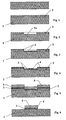
- the figure 1 illustrates a sintered substrate 1 of ZrO 2 , Al 2 O 3 or a mixture of both at the surface of which a layer 2 of a photosensitive polymer is deposited for the formation of a shaped layer for the selective deposition of the patterns.
- the thickness of this layer 2 depends on the variant used to form the patterns, depending on whether they will be substantially surface or raised.
- a mask is applied to this layer 2 of photosensitive polymer type RISTON® MM150, so as to selectively insolve this layer 2 under UV light to polymerize the portions of the layer 2 of photosensitive polymer that must remain on the substrate 1. It then develops this layer 2 in a 0.85% Na 2 CO 3 bath according to the indications of the supplier of the photosensitive polymer, for dissolving the non-insolated portions of the layer 2 to expose portions of surfaces 1a of the substrate 1. These portions present the shapes chosen for the formation of the patterns, as illustrated by the figure 2 . This procedure corresponds to a standard photolithographic process.
- the substrate 1 shown in section by the Figures 1 to 7 is actually a portion of the ceramic element object of the present invention.
- This portion may correspond in particular to a radial section of this ceramic element consisting of a circular ring of rectangular section.
- this ring has a frustoconical shape, so that the visible surface 1a is inclined relative to the axis of revolution of this ring.
- the mask used for forming the patterns in the polymer layer 2 is not a conventional mask, but a polymer mask, thermoformed to give it a shape complementary to that of the ceramic substrate.
- This polymeric mask which has a certain flexibility is applied to the layer 2 with sufficient pressure so that it marries this layer 2 over its entire surface.
- the substrate 1 thus selectively coated with the layer 2 is placed in a vacuum coating chamber, in which a first Ti, Ta, Cr or Th tilting layer 3 is used.
- a first Ti, Ta, Cr or Th tilting layer 3 is used.
- at least 100 nm is deposited ( figure 3 ) by the technique of physical vapor deposition (PVD) and magnetron cathode sputtering which ensures adhesion of the attachment layer 3, greater than that which would be obtained using the PVD technique without magnetron.
- PVD physical vapor deposition
- magnetron cathode sputtering the temperature of the substrate 1 can be kept low, well below 100 ° C during the deposition process.
- a second layer 4 is formed ( figure 4 ) by magnetron sputtering using a target of the type Au, Ag, Pt, Pd, TiN, CrN, Ni ZrN.
- the thickness of this second layer is at least 100 nm, preferably between 500 nm and 15 ⁇ m.
- the pieces were cleaned in an ultrasonic bath in a mixture of 20% isopropyl alcohol and 80% deionized water for five minutes. Drying with a nitrogen gun.
- the substrates thus obtained are entirely covered with the titanium bonding layer covered with the gold layer, as illustrated by the figure 4 .
- the substrate is removed from the vacuum deposition chamber and there is a choice between two solutions.
- the substrate 1 is selectively coated with the polymer layer 2 and the layers 3 and 4 ( figure 4 ), to an electroforming operation, using the same noble metal as used for the second layer 4, in this example, gold.
- the advantage of the invention lies in the ability to keep the polymer mask intact for use in the subsequent selective electroforming operation.
- An additional layer 5 of desired thickness is thus deposited by electroforming. SOE.
- the gold bath used in this case is high in Au and allows electroforming at least 0.10 mm, preferably a few tenths of a millimeter thick.
- the operating conditions of the electroforming process are those indicated by the suppliers of the electroforming bath.
- the duration of the process is a function of the thickness of the deposited layer.
- the growth rate of the deposit is approximately 10 ⁇ m / h.
- the polymer layer 2 is dissolved, as has been done previously to pass from the step of the figure 5 to that of the figure 6 , so that there remains on the substrate 1 only the layers 3 and 4 which were on the parts 1a where the ceramic substrate was not covered by the dissolved polymer layer 2.
- the patterns are substantially on the surface of the substrate 1.
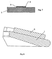
- the ceramic element which is the subject of the present invention, could be in the form of a polygonal frame with a face inclined with respect to the central axis of this element and thus constitute a truncated pyramid.
- the figure 8 illustrates a ceramic ring 1, of frustoconical shape intended to be reported by elastic deformation on a telescope.
- This ring 1 is provided with relief patterns 5, according to the embodiment of the figure 5 .
Description
- La présente invention se rapporte à un procédé de fabrication d'élément en céramique destiné à être rapporté sur une boîte de montre, dont la surface visible comporte des motifs, ainsi qu'à un élément en céramique obtenu par ce procédé.
- Il a déjà été proposé dans le
DE 2'533'524 et dans leEP 0'230'853 un procédé pour déposer une couche métallisée sur un substrat en céramique qui consiste à déposer une première couche de CuO ou de Ti d'au moins 100 nm suivie d'une seconde couche de cuivre, d'argent, d'or ou de nickel. L'adhésion entre les deux couches est obtenue par passage au four. Dans le cas du cuivre et du CuO, la température du four doit se situer entre le point eutectique du CuO et le point de fusion du cuivre soit entre 1068° et 1078°C, température qui est totalement incompatible avec l'utilisation d'une résine photosensible, en sorte que de tels procédés ne permettent pas de garder le masque en vue d'une opération ultérieure d'électroformage. - Etant donné que ces procédés ne permettent pas d'utiliser des matériaux photosensibles, selon des techniques couramment utilisées pour la fabrication de composants électroniques notamment, il ne peuvent donc pas être utilisés pour faire croître sélectivement des motifs tels que des chiffres par électroformage, puisque de tels masques ne résisteraient pas à la température du traitement de fixation des couches au four.
- On a également proposé dans le
CH 636' 238 - Le but de la présente invention est de remédier, au moins en partie, aux inconvénients susmentionnés.
- A cet effet, cette invention a tout d'abord pour objet un procédé de fabrication d'un élément en céramique destiné à être rapporté sur une boîte de montre et dont la surface visible présente des motifs, selon la revendication 1. Elle a ensuite pour objet un élément en céramique, selon la revendication 4.
- L'avantage essentiel de cette invention est de permettre la formation sélective de motifs, sans aucune limitation de forme, donnant naissance à un produit nouveau, offrant des possibilités esthétiques originales, permettant de renouveler et d'améliorer l'aspect des montres, en particulier celui des montres à lunettes fixes et tournantes.
- Le procédé selon la présente invention permet d'obtenir une excellente adhésion des motifs en relief à la surface de l'élément en céramique, ce qui présente une grande importance, surtout lorsque les motifs sont en relief, puisqu'une boîte de montre-bracelet en particulier est très exposée à toutes sortes d'agressions externes notamment aux chocs.
- Avantageusement, la surface visible sur laquelle les motifs sont formés est une surface tronconique ou en forme de tronc de pyramide, qui nécessite de ce fait une technique de masquage particulière.
- D'autres particularités et avantages apparaîtront au cours de la description qui suit et qui sera faite en se référant aux dessins annexés qui illustrent, schématiquement et à titre d'exemple, une forme d'exécution et une variante de la mise en oeuvre du procédé objet de la présente invention, ainsi que les éléments en céramiques obtenus par ce procédé.
- Les
figures 1 à 4 illustrent différentes phases du procédé de préparation d'un élément en céramique vu en coupe, destiné à être rapporté sur une boîte de montre, objet de la présente invention; - les
figures 5 et 6 illustrent une forme d'exécution de formation de motifs en relief; - la
figure 7 illustre une variante pour l'obtention de motifs à la surface de l'élément en céramique; - la
figure 8 est une vue partielle en coupe d'un anneau en céramique pour lunette, selon la présente invention. - La
figure 1 illustre un substrat fritté 1 en ZrO2, Al2O3 ou mélange des deux à la surface duquel une couche 2 d'un polymère photosensible est déposée en vue de la formation d'une couche conformée pour le dépôt sélectif des motifs. L'épaisseur de cette couche 2 dépend de la variante utilisée pour former les motifs, selon que ceux-ci seront sensiblement en surface ou en relief. - On applique un masque sur cette couche 2 de polymère photosensible type RISTON® MM150, de manière à insoler sélectivement cette couche 2 sous une lumière UV pour polymériser les parties de la couche 2 de polymère photosensibles qui doivent rester sur le substrat 1. On développe alors cette couche 2 dans un bain de Na2CO3 à 0,85% selon les indications du fournisseur du polymère photosensible, pour dissoudre les parties non insolées de la couche 2 pour mettre à nu des portions de surfaces 1a du substrat 1. Ces portions présentent les formes choisies pour la formation des motifs, comme illustré par la
figure 2 . Ce mode opératoire correspond à un processus photolithographique standard. - Il y a lieu de remarquer que dans les exemples illustrés, le substrat 1 représenté en coupe par les
figures 1 à 7 correspond en réalité à une portion de l'élément en céramique objet de la présente invention. Cette portion peut correspondre notamment à une section radiale de cet élément en céramique constitué par un anneau circulaire de section rectangulaire. De préférence, cet anneau a une forme tronconique, de sorte que la surface visible 1a est inclinée par rapport à l'axe de révolution de cet anneau. - Pour cette raison, le masque utilisé pour la formation des motifs dans la couche de polymère 2 n'est pas un masque classique, mais un masque en polymère, thermoformé pour lui donner une forme complémentaire à celle du substrat en céramique. Ce masque en polymère qui présente une certaine souplesse est appliqué sur la couche 2 avec une pression suffisante pour qu'il épouse cette couche 2 sur toute sa surface.
- Une fois cette opération de formation des motifs effectuée, on dispose le substrat 1 ainsi revêtu sélectivement par la couche 2, dans une enceinte de revêtement sous vide, dans laquelle une première couche d'accrochage 3 de Ti, Ta, Cr ou Th d'au moins 100 nm est déposée (
figure 3 ) par la technique de dépôt physique en phase vapeur (PVD) et pulvérisation cathodique magnétron qui permet d'assurer une adhésion de la couche d'accrochage 3, supérieure à celle qui serait obtenue en utilisant la technique PVD sans magnétron. En outre, grâce à la pulvérisation cathodique magnétron, la température du substrat 1 peut être maintenue basse, bien en dessous de 100°C pendant l'opération de dépôt. C'est grâce à l'utilisation de cette technique de dépôt qu'il est possible d'effectuer le dépôt de la couche d'accrochage sur le substrat 1 revêtu sélectivement de la couche de polymère 2 et d'assurer une excellente adhésion de cette couche d'accrochage 3 au substrat 1, sans devoir effectuer un traitement thermique à une température amenant à la destruction le polymère. - Tout en maintenant le vide dans l'enceinte de dépôt, on forme une seconde couche 4 (
figure 4 ) par pulvérisation cathodique magnétron en utilisant une cible du type Au, Ag, Pt, Pd, TiN, CrN, Ni ZrN. L'épaisseur de cette seconde couche est d'au moins 100 nm, de préférence, comprise entre 500 nm et 15 µm. - L'équipement utilisé pour effectuer le dépôt sous vide par pulvérisation cathodique au magnétron comprend:
- une enceinte cylindrique en acier inoxydable avec système de pompage turbomoléculaire et pompe rotative à palettes;
- un porte-substrat de type carrousel à axe de rotation vertical et substrats positionnés verticalement. Possibilité de réaliser une pulvérisation cathodique RF polarisée sur le porte-substrat;
- deux cathodes magnétrons rectangulaires verticales montées face au carrousel selon un angle de 120° par rapport à l'axe du carrousel;
- deux cathodes:
- une cible Ti99,99
- une cible Au99,99
- une alimentation des cathodes par un générateur RF 13,56 MHz de 600 W avec une boîte d'accord d'impédance manuel;
- une alimentation en gaz (pureté: 5,7-6,0) par débitmètre de masse;
- un contrôle de pression par jauge Penning pour le contrôle du vide limite et par jauge capacitive (mesure absolue) pour le contrôle de la pression de travail.
- Les pièces ont été nettoyées dans un bain aux ultrasons dans un mélange de 20% d'alcool isopropylique et de 80% d'eau déionisée, pendant cinq minutes. Séchage au pistolet à azote.
- Les substrats sont décapés par mise sous vide de l'enceinte et pompage jusqu'à une pression inférieure à 5 x 10⁻² Pa. Un nettoyage ionique de la surface des substrats est exécuté par pulvérisation inversée:
- puissance RF sur porte-substrat:> 100 W
- flux d'argon:> 15 cm3/min
- flux d'oxygène:> 5 cm3/min
- pression totale:< 5 Pa
- durée: 20-30 min
- Les conditions de dépôt de la sous-couche de titane sont les suivantes:
- puissance RF sur la cathode:> 150 W
- flux d'argon:> 5 cm3/min
- pression d'argon:< 5 Pa
- l'épaisseur de la couche est >100 nm, de préférence >100 nm et <1500 nm
- Tout en maintenant le vide dans l'enceinte, les substrats sont déplacés par rotation du carrousel vers une petite cathode équipée de la cible Au99,99. Les conditions du dépôt sont les suivantes:
- puissance RF sur la cathode:> 50 W
- flux d'argon:> 10 cm3/min
- pression d'argon:< 5 Pa
- l'épaisseur de la couche est >100 nm, de préférence, >500 nm et <15 µm
- Les substrats ainsi obtenus sont entièrement recouverts de la couche d'accrochage en titane recouverte de la couche d'or, comme illustré par la
figure 4 . - Suite au dépôt de cette seconde couche 4, on sort le substrat de l'enceinte de dépôt sous vide et on a le choix entre deux solutions.
- Selon une première forme d'exécution, on soumet le substrat 1 sélectivement revêtu de la couche de polymère 2 et des couches 3 et 4 (
figure 4 ), à une opération d'électroformage, en utilisant le même métal noble que celui utilisé pour la seconde couche 4, dans cet exemple, l'or. Tout l'avantage de l'invention réside dans le pouvoir de garder le masque polymère intact pour son utilisation dans l'opération ultérieure d'électroformage sélectif. On dépose donc par électroformage une couche supplémentaire 5 d'épaisseur désirée. rée. Le bain d'or utilisé dans ce cas est à forte teneur en Au et permet un électroformage d'au moins 0,10 mm, de préférence, de quelque dixièmes de millimètres d'épaisseur. Les condition opératoires du processus d'électroformage sont celles indiquées par les fournisseurs du bain d'électroformage. La durée du processus est fonction de l'épaisseur de la couche déposée. La vitesse de croissance du dépôt est d'environ 10 µm/h. - Selon une deuxième forme d'exécution illustrée par la
figure 7 , après la sortie du substrat revêtu sélectivement des couches 3 et 4, on dissout la couche de polymère 2, comme on l'a fait précédemment pour passer de l'étape de lafigure 5 à celle de lafigure 6 , en sorte qu'il ne reste sur le substrat 1 que les couches 3 et 4 qui se trouvaient sur les parties 1a où le substrat en céramique n'était pas recouvert par la couche de polymère 2 dissoute. Dans ce cas, compte tenu de l'épaisseur des couches 3, 4, les motifs sont pratiquement à la surface du substrat 1. - En variante, au lieu d'être en forme d'anneau tronconique, l'élément en céramique, objet de la présente invention, pourrait être en forme de cadre polygonal à face inclinée par rapport à l'axe central de cet élément et constituer ainsi un tronc de pyramide.
- La
figure 8 illustre un anneau en céramique 1, de forme tronconique destiné à être rapporté par déformation élastique sur une lunette. Cet anneau 1 est muni de motifs en relief 5, selon la forme d'exécution de lafigure 5 .
Claims (9)
- Procédé de fabrication d'élément en céramique destiné à être rapporté sur une boîte de montre et dont la surface visible présente des motifs, caractérisé en ce que l'on dépose sélectivement sur ladite surface visible une couche soluble de polymère photosensible (2) dont l'épaisseur est au moins égale à la hauteur desdits motifs, on dépose sous vide sur ladite surface ainsi recouverte sélectivement une première couche d'accrochage (3) de type Ti, Ta, Cr ou Th d'au moins 100 nm par dépôt physique en phase vapeur (PVD) avec pulvérisation cathodique magnétron suivie, sans mise à l'air, d'un dépôt PVD de ladite seconde couche (4) de Au, Pt, Ag, Ni, Pd, TiN, CrN, ZrN ou leurs alliages d'au moins 100 nm d'épaisseur et on dissout ladite couche soluble (2).
- Procédé selon la revendication 1 selon lequel, avant de dissoudre ladite couche soluble (2), on dépose une couche supplémentaire (5) d'un métal noble ou alliage de métaux nobles par électroformage.
- Procédé selon la revendication 2, selon lequel on applique sur ladite couche (2) de polymère photosensible un masque en polymère thermoplastique réalisé par thermoformage.
- Elément en céramique destiné à être rapporté sur une boîte de montre et dont la surface visible présente des motifs caractérisé en ce que ces motifs sont fixés sur cette surface par une première couche d'accrochage (3) de Ti, Ta, Cr ou Th d'au moins 100 nm, recouverte d'au moins une seconde couche (4) du groupe Au, Ag, CrN, Ni, Pt, TiN, ZrN, Pd ou leurs alliages d'au moins 100 nm d'épaisseur.
- Elément en céramique selon la revendication 4, dont la forme est circulaire avec la face formant ladite surface visible de forme tronconique.
- Elément en céramique selon la revendication 4, dont la forme est celle d'un cadre polygonal avec la face formant ladite surface visible en forme de tronc de pyramide.
- Elément en céramique selon l'une des revendications 4 à 6, dans lequel ladite céramique est du ZrO2, de l'Al2O3 ou un mélange des deux.
- Elément en céramique selon l'une des revendications 4 à 7, dans lequel, lesdits motifs sont formés par une couche supplémentaire (5) d'au moins 0,10 mm d'épaisseur, du même métal ou alliage que ladite seconde couche (4).
- Boîte de montre comprenant élément en céramique selon l'une des revendications 4 à 8.
Priority Applications (7)
| Application Number | Priority Date | Filing Date | Title |
|---|---|---|---|
| EP03405924.6A EP1548525B2 (fr) | 2003-12-23 | 2003-12-23 | Elément en céramique pour boîte de montre et procédé de fabrication de cet élément |
| CNB2004100819067A CN100507765C (zh) | 2003-12-23 | 2004-12-16 | 制造用于表壳的陶瓷元件的方法及通过该方法获得的元件 |
| JP2004371658A JP2005181341A (ja) | 2003-12-23 | 2004-12-22 | 時計ケース用セラミック部材の製造方法及びその方法により得られる部材 |
| US11/061,289 US7628894B2 (en) | 2003-12-23 | 2005-02-18 | Process for manufacturing a ceramic element for a watch case and element obtained by this process |
| HK05105899A HK1073506A1 (en) | 2003-12-23 | 2005-07-12 | Ceramic element for watch case and method of manufacturing the same |
| US12/603,792 US8282270B2 (en) | 2003-12-23 | 2009-10-22 | Process for manufacturing a ceramic element for a watch case and element obtained by this process |
| JP2011138570A JP4921603B2 (ja) | 2003-12-23 | 2011-06-22 | 時計ケース用セラミック部材の製造方法及びその方法により得られる部材 |
Applications Claiming Priority (1)
| Application Number | Priority Date | Filing Date | Title |
|---|---|---|---|
| EP03405924.6A EP1548525B2 (fr) | 2003-12-23 | 2003-12-23 | Elément en céramique pour boîte de montre et procédé de fabrication de cet élément |
Publications (3)
| Publication Number | Publication Date |
|---|---|
| EP1548525A1 EP1548525A1 (fr) | 2005-06-29 |
| EP1548525B1 true EP1548525B1 (fr) | 2013-08-14 |
| EP1548525B2 EP1548525B2 (fr) | 2017-08-16 |
Family
ID=34530866
Family Applications (1)
| Application Number | Title | Priority Date | Filing Date |
|---|---|---|---|
| EP03405924.6A Expired - Lifetime EP1548525B2 (fr) | 2003-12-23 | 2003-12-23 | Elément en céramique pour boîte de montre et procédé de fabrication de cet élément |
Country Status (5)
| Country | Link |
|---|---|
| US (2) | US7628894B2 (fr) |
| EP (1) | EP1548525B2 (fr) |
| JP (2) | JP2005181341A (fr) |
| CN (1) | CN100507765C (fr) |
| HK (1) | HK1073506A1 (fr) |
Families Citing this family (16)
| Publication number | Priority date | Publication date | Assignee | Title |
|---|---|---|---|---|
| US8553364B1 (en) | 2005-09-09 | 2013-10-08 | Magnecomp Corporation | Low impedance, high bandwidth disk drive suspension circuit |
| US7781679B1 (en) * | 2005-09-09 | 2010-08-24 | Magnecomp Corporation | Disk drive suspension via formation using a tie layer and product |
| US7829793B2 (en) * | 2005-09-09 | 2010-11-09 | Magnecomp Corporation | Additive disk drive suspension manufacturing using tie layers for vias and product thereof |
| US8395866B1 (en) | 2005-09-09 | 2013-03-12 | Magnecomp Corporation | Resilient flying lead and terminus for disk drive suspension |
| CH714243B1 (fr) * | 2006-10-03 | 2019-04-15 | Swatch Group Res & Dev Ltd | Procédé d'électroformage et pièce ou couche obtenue par ce procédé. |
| CH710184B1 (fr) | 2007-09-21 | 2016-03-31 | Aliprandini Laboratoires G | Procédé d'obtention d'un dépôt d'alliage d'or jaune par galvanoplastie sans utilisation de métaux ou métalloïdes toxiques. |
| EP2312021B1 (fr) | 2009-10-15 | 2020-03-18 | The Swatch Group Research and Development Ltd. | Procédé d'obtention d'un dépôt d'alliage d'or jaune par galvanoplastie sans utilisation de métaux toxiques |
| WO2013131943A1 (fr) * | 2012-03-07 | 2013-09-12 | Seco Tools Ab | Corps avec une couche de nitrure à base de métal et procédé pour revêtir le corps |
| CN102912292B (zh) * | 2012-10-18 | 2014-05-28 | 东南大学 | 用于镍基合金紧固件表面的抗高温粘结涂层及其制备方法 |
| US9284485B2 (en) | 2012-11-07 | 2016-03-15 | Rolex Sa | Persistent phosphorescent composite material |
| CN103572233B (zh) * | 2013-10-16 | 2015-09-23 | 中国科学院宁波材料技术与工程研究所 | 一种贵金属陶瓷薄膜及其制备方法 |
| EP3088372B1 (fr) | 2013-12-27 | 2021-03-10 | Tosoh Corporation | Corps fritté de zircone et son utilisation |
| EP3034461B1 (fr) * | 2014-12-19 | 2020-07-01 | Rolex Sa | Fabrication d'un composant horloger multi-niveaux |
| FR3077302B1 (fr) * | 2018-01-29 | 2019-12-27 | Avipo | Depot de pvd en fond de gravure |
| CH714739A2 (fr) * | 2018-03-09 | 2019-09-13 | Swatch Group Res & Dev Ltd | Procédé de fabrication d’un décor métallique sur un cadran et cadran obtenu selon ce procédé. |
| EP3575447A1 (fr) * | 2018-05-28 | 2019-12-04 | The Swatch Group Research and Development Ltd | Procede de fabrication d'un decor metallique sur un cadran et cadran obtenu selon ce procede |
Citations (17)
| Publication number | Priority date | Publication date | Assignee | Title |
|---|---|---|---|---|
| DE2533524A1 (de) † | 1975-07-26 | 1977-03-10 | Licentia Gmbh | Verfahren zur haftfesten metallisierung eines traegerkoerpers und damit erhaltener gegenstand |
| US4213840A (en) † | 1978-11-13 | 1980-07-22 | Avantek, Inc. | Low-resistance, fine-line semiconductor device and the method for its manufacture |
| US4226082A (en) † | 1976-06-07 | 1980-10-07 | Nobuo Nishida | Ornamental part for watches and method of producing the same |
| JPS60141647A (ja) † | 1983-12-27 | 1985-07-26 | Seiko Instr & Electronics Ltd | カバ−ガラスの加飾方法 |
| EP0221492A2 (fr) † | 1985-11-04 | 1987-05-13 | Asulab S.A. | Objet pourvu d'un revêtement en métal précieux résistant à l'usure |
| WO1987004812A1 (fr) † | 1986-02-04 | 1987-08-13 | Preci-Coat S.A. | Procede de depot sur un substrat, d'une couche d'un revetement decoratif resistant a l'usure, et objet realise selon ce procede |
| US4699850A (en) † | 1985-03-19 | 1987-10-13 | Seiko Instruments & Electronics Ltd. | Ornamental part |
| US4943486A (en) † | 1987-04-01 | 1990-07-24 | Seiko Epson Corporation | Coated article and method of production |
| WO1991014017A1 (fr) † | 1990-03-09 | 1991-09-19 | Kennametal Inc. | Deposition en phase gazeuse par procede physique de nitrure de titane sur un substrat non-conducteur |
| JPH046263A (ja) † | 1990-04-24 | 1992-01-10 | Namiki Precision Jewel Co Ltd | サファイヤヘの貴金属加飾方法 |
| JPH0725199A (ja) † | 1993-07-12 | 1995-01-27 | Namiki Precision Jewel Co Ltd | サファイヤへの貴金属加飾方法 |
| EP0686706A1 (fr) † | 1993-12-28 | 1995-12-13 | Citizen Watch Co. Ltd. | Piece decorative blanche et procede pour sa fabrication |
| US5972233A (en) † | 1996-01-31 | 1999-10-26 | Refractal Design, Inc. | Method of manufacturing a decorative article |
| EP1286234A1 (fr) † | 2000-04-20 | 2003-02-26 | Trigger Co., Ltd. | Boitier haute frequence pour montre-bracelet |
| JP2003253473A (ja) † | 2001-12-28 | 2003-09-10 | Citizen Watch Co Ltd | 白色被膜を有する装飾品およびその製造方法 |
| JP2003268568A (ja) † | 2002-01-09 | 2003-09-25 | Citizen Watch Co Ltd | 白色被膜を有する装飾品およびその製造方法 |
| CH702127B1 (fr) † | 2007-05-25 | 2011-05-13 | Paul Hartzband | Pièce d'horlogerie munie d'un tour d'heures variable. |
Family Cites Families (26)
| Publication number | Priority date | Publication date | Assignee | Title |
|---|---|---|---|---|
| CH67374A4 (fr) * | 1974-01-18 | 1975-09-15 | ||
| JPS55141569A (en) * | 1979-04-24 | 1980-11-05 | Kawaguchiko Seimitsu Kk | Manufacture of dial plate of watch |
| JPS55135769A (en) * | 1979-04-11 | 1980-10-22 | Kawaguchiko Seimitsu Kk | Manufacture of dial for watch |
| CH641313GA3 (fr) * | 1980-05-31 | 1984-02-29 | ||
| US4397566A (en) * | 1982-05-04 | 1983-08-09 | Montres Rado S.A. | Wrist-watch casing |
| US4512863A (en) * | 1983-09-09 | 1985-04-23 | Ppg Industries, Inc. | Stainless steel primer for sputtered films |
| US4565616A (en) * | 1984-04-30 | 1986-01-21 | Ppg Industries, Inc. | Method for producing a photoelectroforming mandrel |
| EP0230853A1 (fr) * | 1986-01-20 | 1987-08-05 | W. Blösch AG | Procédé de fabrication d'une couche brasable d'un alliage sur un substrat céramique, de préférence céramique d'oxydes |
| US5100714A (en) * | 1986-07-24 | 1992-03-31 | Ceramic Packaging, Inc. | Metallized ceramic substrate and method therefor |
| US5058799A (en) * | 1986-07-24 | 1991-10-22 | Zsamboky Kalman F | Metallized ceramic substrate and method therefor |
| US4886766A (en) * | 1987-08-10 | 1989-12-12 | Lanxide Technology Company, Lp | Method of making ceramic composite articles and articles made thereby |
| US5082700A (en) * | 1987-08-10 | 1992-01-21 | Lanxide Technology Company, Lp | Method of making ceramic composite articles and articles made thereby |
| JPH0192356A (ja) * | 1987-09-30 | 1989-04-11 | Pentel Kk | 装飾体およびその製造方法 |
| US5157258A (en) * | 1989-08-21 | 1992-10-20 | Rockwell International Corporation | Multicolor infrared focal plane arrays |
| DE4009151A1 (de) * | 1990-03-22 | 1991-09-26 | Leybold Ag | Vorrichtung zum beschichten von substraten durch katodenzerstaeubung |
| US5358597A (en) * | 1991-09-04 | 1994-10-25 | Gte Laboratories Incorporated | Method of protecting aluminum nitride circuit substrates during electroless plating using sol-gel oxide films and article made therefrom |
| US5331608A (en) * | 1992-03-31 | 1994-07-19 | Citizen Watch Co., Ltd. | Electronic watch with an antenna for a receiving device |
| DE4213041C1 (fr) * | 1992-04-21 | 1993-06-09 | W.C. Heraeus Gmbh, 6450 Hanau, De | |
| CN1093274C (zh) * | 1995-04-07 | 2002-10-23 | 时至准钟表股份有限公司 | 太阳能电池表的字盘 |
| JPH09127261A (ja) * | 1995-11-01 | 1997-05-16 | Kawaguchiko Seimitsu Kk | 時計用文字板 |
| EP0844539B1 (fr) * | 1996-11-22 | 2003-11-19 | Montres Rado S.A. | Elément décoratif, notamment élément constitutif d'une pièce d'horlogerie |
| US6502982B1 (en) * | 1998-06-05 | 2003-01-07 | Montres Rado Sa | Structural component made of hard material for a wristwatch |
| JP3957920B2 (ja) * | 1998-06-11 | 2007-08-15 | キヤノン株式会社 | インクジェットヘッドの製造方法 |
| TW517180B (en) * | 2001-02-23 | 2003-01-11 | Swatch Group Man Serv Ag | Timepiece with analogue display of time related information based on a decimal system |
| TW589167B (en) * | 2001-08-29 | 2004-06-01 | Rado Montres Sa | Link for watch bracelet |
| WO2003056966A1 (fr) * | 2001-12-28 | 2003-07-17 | Citizen Watch Co., Ltd. | Objet decoratif presentant un revetement blanc et son procede de fabrication |
-
2003
- 2003-12-23 EP EP03405924.6A patent/EP1548525B2/fr not_active Expired - Lifetime
-
2004
- 2004-12-16 CN CNB2004100819067A patent/CN100507765C/zh active Active
- 2004-12-22 JP JP2004371658A patent/JP2005181341A/ja not_active Withdrawn
-
2005
- 2005-02-18 US US11/061,289 patent/US7628894B2/en active Active
- 2005-07-12 HK HK05105899A patent/HK1073506A1/xx not_active IP Right Cessation
-
2009
- 2009-10-22 US US12/603,792 patent/US8282270B2/en active Active
-
2011
- 2011-06-22 JP JP2011138570A patent/JP4921603B2/ja active Active
Patent Citations (17)
| Publication number | Priority date | Publication date | Assignee | Title |
|---|---|---|---|---|
| DE2533524A1 (de) † | 1975-07-26 | 1977-03-10 | Licentia Gmbh | Verfahren zur haftfesten metallisierung eines traegerkoerpers und damit erhaltener gegenstand |
| US4226082A (en) † | 1976-06-07 | 1980-10-07 | Nobuo Nishida | Ornamental part for watches and method of producing the same |
| US4213840A (en) † | 1978-11-13 | 1980-07-22 | Avantek, Inc. | Low-resistance, fine-line semiconductor device and the method for its manufacture |
| JPS60141647A (ja) † | 1983-12-27 | 1985-07-26 | Seiko Instr & Electronics Ltd | カバ−ガラスの加飾方法 |
| US4699850A (en) † | 1985-03-19 | 1987-10-13 | Seiko Instruments & Electronics Ltd. | Ornamental part |
| EP0221492A2 (fr) † | 1985-11-04 | 1987-05-13 | Asulab S.A. | Objet pourvu d'un revêtement en métal précieux résistant à l'usure |
| WO1987004812A1 (fr) † | 1986-02-04 | 1987-08-13 | Preci-Coat S.A. | Procede de depot sur un substrat, d'une couche d'un revetement decoratif resistant a l'usure, et objet realise selon ce procede |
| US4943486A (en) † | 1987-04-01 | 1990-07-24 | Seiko Epson Corporation | Coated article and method of production |
| WO1991014017A1 (fr) † | 1990-03-09 | 1991-09-19 | Kennametal Inc. | Deposition en phase gazeuse par procede physique de nitrure de titane sur un substrat non-conducteur |
| JPH046263A (ja) † | 1990-04-24 | 1992-01-10 | Namiki Precision Jewel Co Ltd | サファイヤヘの貴金属加飾方法 |
| JPH0725199A (ja) † | 1993-07-12 | 1995-01-27 | Namiki Precision Jewel Co Ltd | サファイヤへの貴金属加飾方法 |
| EP0686706A1 (fr) † | 1993-12-28 | 1995-12-13 | Citizen Watch Co. Ltd. | Piece decorative blanche et procede pour sa fabrication |
| US5972233A (en) † | 1996-01-31 | 1999-10-26 | Refractal Design, Inc. | Method of manufacturing a decorative article |
| EP1286234A1 (fr) † | 2000-04-20 | 2003-02-26 | Trigger Co., Ltd. | Boitier haute frequence pour montre-bracelet |
| JP2003253473A (ja) † | 2001-12-28 | 2003-09-10 | Citizen Watch Co Ltd | 白色被膜を有する装飾品およびその製造方法 |
| JP2003268568A (ja) † | 2002-01-09 | 2003-09-25 | Citizen Watch Co Ltd | 白色被膜を有する装飾品およびその製造方法 |
| CH702127B1 (fr) † | 2007-05-25 | 2011-05-13 | Paul Hartzband | Pièce d'horlogerie munie d'un tour d'heures variable. |
Also Published As
| Publication number | Publication date |
|---|---|
| HK1073506A1 (en) | 2005-10-07 |
| CN100507765C (zh) | 2009-07-01 |
| EP1548525A1 (fr) | 2005-06-29 |
| CN1637662A (zh) | 2005-07-13 |
| US20060011471A1 (en) | 2006-01-19 |
| US7628894B2 (en) | 2009-12-08 |
| JP2011191321A (ja) | 2011-09-29 |
| EP1548525B2 (fr) | 2017-08-16 |
| JP2005181341A (ja) | 2005-07-07 |
| US20100110841A1 (en) | 2010-05-06 |
| US8282270B2 (en) | 2012-10-09 |
| JP4921603B2 (ja) | 2012-04-25 |
Similar Documents
| Publication | Publication Date | Title |
|---|---|---|
| EP1548525B1 (fr) | Elément en céramique pour boîte de montre et procédé de fabrication de cet élément | |
| EP1548524B1 (fr) | Elément en céramique pour boîte de montre et procédé de fabrication de cet élément | |
| EP0038294B1 (fr) | Procédé de dépôt d'un revêtement dur métallique, cible de dépôt pour un tel procédé et pièce de joaillerie comportant un tel revêtement | |
| EP0119459B1 (fr) | Pièce comprenant un substrat muni d'un revêtement dur et résistance à la corrosion | |
| EP2767870B1 (fr) | Procédé de fabrication d'une pièce de micromécanique monobloc comportant au moins deux niveaux fonctionnels distincts | |
| EP2354083B1 (fr) | Procédé d'encapsulation d'un microcomposant par un capot renforce mécaniquement | |
| EP3339980A1 (fr) | Procédé de réalisation d'un motif sur une pièce horlogère et pièce horlogère | |
| EP3708384A1 (fr) | Element d'habillage ou cadran d'horlogerie ou de bijouterie en materiau conducteur | |
| EP2659307B1 (fr) | Procédé de fabrication d'objets de grande précision par lithographie haute résolution et par dépôt par voie sèche et objets ainsi obtenus | |
| EP3078436A1 (fr) | Procede de fabrication d'un composant horloger | |
| EP1672436B1 (fr) | Cadran pour pièce d'horlogerie et procédés de fabrication de ce cadran | |
| EP0627330B1 (fr) | Procédé d'obtention d'une empreinte gravée pourvue d'un matériau de contraste | |
| EP3764169B1 (fr) | Procede pour depolir par endroits un composant horloger en silicium | |
| CH710716A2 (fr) | Procédé de fabrication d'une pièce avec au moins un décor. | |
| JP4909477B2 (ja) | 装飾部材及び装飾部材の製造方法 | |
| CH715191B1 (fr) | Procédé de décoration d'un composant d'habillage en horlogerie. | |
| EP0411079B1 (fr) | Procede de depot d'au moins une epaisseur d'au moins un materiau decoratif sur un objet et objet decoratif realise selon ce procede | |
| CH720105A2 (fr) | Procédé de fabrication d'un composant horloger | |
| EP2833204A1 (fr) | Procede de traitement d'une couche de resine photosensible et procede de fabrication d'un composant metallique | |
| JPH1172577A (ja) | 外装部材の製造方法及び電子機器 |
Legal Events
| Date | Code | Title | Description |
|---|---|---|---|
| PUAI | Public reference made under article 153(3) epc to a published international application that has entered the european phase |
Free format text: ORIGINAL CODE: 0009012 |
|
| AK | Designated contracting states |
Kind code of ref document: A1 Designated state(s): AT BE BG CH CY CZ DE DK EE ES FI FR GB GR HU IE IT LI LU MC NL PT RO SE SI SK TR |
|
| AX | Request for extension of the european patent |
Extension state: AL LT LV MK |
|
| REG | Reference to a national code |
Ref country code: HK Ref legal event code: DE Ref document number: 1073506 Country of ref document: HK |
|
| 17P | Request for examination filed |
Effective date: 20050922 |
|
| AKX | Designation fees paid |
Designated state(s): CH DE FR GB LI |
|
| 17Q | First examination report despatched |
Effective date: 20070720 |
|
| GRAP | Despatch of communication of intention to grant a patent |
Free format text: ORIGINAL CODE: EPIDOSNIGR1 |
|
| GRAP | Despatch of communication of intention to grant a patent |
Free format text: ORIGINAL CODE: EPIDOSNIGR1 |
|
| GRAS | Grant fee paid |
Free format text: ORIGINAL CODE: EPIDOSNIGR3 |
|
| GRAA | (expected) grant |
Free format text: ORIGINAL CODE: 0009210 |
|
| AK | Designated contracting states |
Kind code of ref document: B1 Designated state(s): CH DE FR GB LI |
|
| REG | Reference to a national code |
Ref country code: GB Ref legal event code: FG4D Free format text: NOT ENGLISH |
|
| REG | Reference to a national code |
Ref country code: CH Ref legal event code: EP |
|
| REG | Reference to a national code |
Ref country code: CH Ref legal event code: NV Representative=s name: MOINAS AND SAVOYE SA, CH |
|
| REG | Reference to a national code |
Ref country code: DE Ref legal event code: R096 Ref document number: 60344711 Country of ref document: DE Effective date: 20131010 |
|
| REG | Reference to a national code |
Ref country code: HK Ref legal event code: GR Ref document number: 1073506 Country of ref document: HK |
|
| PLBI | Opposition filed |
Free format text: ORIGINAL CODE: 0009260 |
|
| 26 | Opposition filed |
Opponent name: G. ET F. CHATELAIN SA Effective date: 20140514 |
|
| PLAX | Notice of opposition and request to file observation + time limit sent |
Free format text: ORIGINAL CODE: EPIDOSNOBS2 |
|
| REG | Reference to a national code |
Ref country code: DE Ref legal event code: R026 Ref document number: 60344711 Country of ref document: DE Effective date: 20140514 |
|
| PLBB | Reply of patent proprietor to notice(s) of opposition received |
Free format text: ORIGINAL CODE: EPIDOSNOBS3 |
|
| REG | Reference to a national code |
Ref country code: FR Ref legal event code: PLFP Year of fee payment: 13 |
|
| REG | Reference to a national code |
Ref country code: CH Ref legal event code: PFA Owner name: ROLEX SA, CH Free format text: FORMER OWNER: ROLEX SA, CH |
|
| REG | Reference to a national code |
Ref country code: FR Ref legal event code: PLFP Year of fee payment: 14 |
|
| PUAH | Patent maintained in amended form |
Free format text: ORIGINAL CODE: 0009272 |
|
| STAA | Information on the status of an ep patent application or granted ep patent |
Free format text: STATUS: PATENT MAINTAINED AS AMENDED |
|
| 27A | Patent maintained in amended form |
Effective date: 20170816 |
|
| AK | Designated contracting states |
Kind code of ref document: B2 Designated state(s): CH DE FR GB LI |
|
| REG | Reference to a national code |
Ref country code: DE Ref legal event code: R102 Ref document number: 60344711 Country of ref document: DE |
|
| REG | Reference to a national code |
Ref country code: CH Ref legal event code: AELC |
|
| REG | Reference to a national code |
Ref country code: FR Ref legal event code: PLFP Year of fee payment: 15 |
|
| PGFP | Annual fee paid to national office [announced via postgrant information from national office to epo] |
Ref country code: GB Payment date: 20221219 Year of fee payment: 20 Ref country code: FR Payment date: 20221220 Year of fee payment: 20 Ref country code: DE Payment date: 20220624 Year of fee payment: 20 |
|
| PGFP | Annual fee paid to national office [announced via postgrant information from national office to epo] |
Ref country code: CH Payment date: 20221229 Year of fee payment: 20 |
|
| P01 | Opt-out of the competence of the unified patent court (upc) registered |
Effective date: 20230528 |
|
| REG | Reference to a national code |
Ref country code: DE Ref legal event code: R071 Ref document number: 60344711 Country of ref document: DE |
|
| REG | Reference to a national code |
Ref country code: CH Ref legal event code: PL |
|
| REG | Reference to a national code |
Ref country code: GB Ref legal event code: PE20 Expiry date: 20231222 |
|
| PG25 | Lapsed in a contracting state [announced via postgrant information from national office to epo] |
Ref country code: GB Free format text: LAPSE BECAUSE OF EXPIRATION OF PROTECTION Effective date: 20231222 |
|
| PG25 | Lapsed in a contracting state [announced via postgrant information from national office to epo] |
Ref country code: GB Free format text: LAPSE BECAUSE OF EXPIRATION OF PROTECTION Effective date: 20231222 |