EP1547246B1 - Integrierte schaltung mit automatischer polaritätsdetektion und konfiguration - Google Patents
Integrierte schaltung mit automatischer polaritätsdetektion und konfiguration Download PDFInfo
- Publication number
- EP1547246B1 EP1547246B1 EP03752479A EP03752479A EP1547246B1 EP 1547246 B1 EP1547246 B1 EP 1547246B1 EP 03752479 A EP03752479 A EP 03752479A EP 03752479 A EP03752479 A EP 03752479A EP 1547246 B1 EP1547246 B1 EP 1547246B1
- Authority
- EP
- European Patent Office
- Prior art keywords
- state
- mute
- node
- output
- input
- Prior art date
- Legal status (The legal status is an assumption and is not a legal conclusion. Google has not performed a legal analysis and makes no representation as to the accuracy of the status listed.)
- Expired - Lifetime
Links
- 238000001514 detection method Methods 0.000 title description 3
- 238000000034 method Methods 0.000 claims description 9
- 230000003213 activating effect Effects 0.000 claims description 2
- 230000008878 coupling Effects 0.000 claims 2
- 238000010168 coupling process Methods 0.000 claims 2
- 238000005859 coupling reaction Methods 0.000 claims 2
- 238000010586 diagram Methods 0.000 description 4
- 239000007795 chemical reaction product Substances 0.000 description 2
- 230000010355 oscillation Effects 0.000 description 1
- 230000000717 retained effect Effects 0.000 description 1
Images



Classifications
-
- H—ELECTRICITY
- H03—ELECTRONIC CIRCUITRY
- H03K—PULSE TECHNIQUE
- H03K19/00—Logic circuits, i.e. having at least two inputs acting on one output; Inverting circuits
-
- H—ELECTRICITY
- H03—ELECTRONIC CIRCUITRY
- H03F—AMPLIFIERS
- H03F3/00—Amplifiers with only discharge tubes or only semiconductor devices as amplifying elements
- H03F3/20—Power amplifiers, e.g. Class B amplifiers, Class C amplifiers
- H03F3/21—Power amplifiers, e.g. Class B amplifiers, Class C amplifiers with semiconductor devices only
- H03F3/217—Class D power amplifiers; Switching amplifiers
- H03F3/2171—Class D power amplifiers; Switching amplifiers with field-effect devices
-
- G—PHYSICS
- G01—MEASURING; TESTING
- G01R—MEASURING ELECTRIC VARIABLES; MEASURING MAGNETIC VARIABLES
- G01R19/00—Arrangements for measuring currents or voltages or for indicating presence or sign thereof
- G01R19/14—Indicating direction of current; Indicating polarity of voltage
Definitions
- the present invention relates generally to the field of integrated circuits and, in particular, to detecting and configuring the required polarity of a circuit pin.
- An integrated circuit or "chip” is generally installed or mounted on a system board which is ultimately installed in an end product.
- an integrated circuit may be purchased for use in several (or many) different end products, often by different manufacturers. It will be appreciated that it may be impractical to use separate chip designs for similar applications. However, in the past, it has also been impractical to automatically modify chips so as to function with a variety of different system boards.
- audio devices such as DVD units and audio/video (A/V) receivers include a digital audio integrated circuit having, among other functional components, a digital-to-analog converter (DAC) for outputting an analog audio reproduction of a digital signal.
- the integrated circuit is mounted on a system board which generally includes a mute circuit to disable the analog audio output during unit power-on, reset or other predetermined events. Absent such mute, the listener would hear clicks and pops which are both distracting to the listener and potentially damaging to the audio device or speakers.
- clicks and pops may still be generated downstream from the DAC, especially as there may be some brief, but finite, time delay after the 0s begin to be input to the DAC.
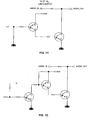
- Figures 1A-1D are examples of mute circuits commonly used on system boards.
- the circuits of Figs. 1A and 1C are activated when the mute signal (actually the inverted mute signal) to the "mute node" is in a low state, driving the mute node to ground; these circuits are said to have an "active low mute”.
- the circuits of Figs. 1B and 1D have an active high mute and are activated when the control signal to the mute node is in a high state.
- the mute circuits is activated by mute driver circuitry on the audio chip which, In turn, is enabled by a mute_control signal 202.
- Fig. 2 is an illustration of a typical prior art mute driver circuit 200.
- transistor M0 is off and M1 is on, driving the mute node 204 high.
- transistor MO is on and M1 is off, driving the mute node 204 low.
- the signal to the mute node 204 must either be high or low.
- the designer of the audio chip must either know In advance with which type of mute circuit the chip will be used and make available the appropriate chip or the system board designer must decide in advance which chip will be used and conform the mute circuit to the chip (and then be limited as to second or future sources of the chip).
- the chip may be designed with configurable polarity.
- configurable polarity requires either an extra and dedicated pin or a register which can be set through a control port whenever the chip goes through a power-on or reset.
- One disadvantage to using a register is that there may still be a delay after the chip exits the reset state until the register is configured. During this time the mute node may be In the unmute state, resulting in the undesirable clicks and pops which were to be eliminated.
- US 5,371,455 discloses a control circuit for safe charging a rechargeable battery, the control circuit comprises a forced short-circuit switch, a safety switch, an automatic change switch, a first rectification circuit, a second rectification circuit, a reverse-polarity detection circuit, a charging-signal output circuit, an oscillation circuit, and a condition-indicating signal assembly.
- Power supply can be provided from a conventional charging device or a spare battery.
- the reverse-polarity detection circuit is used for detecting the correct polarity connection; when reverse polarity is connected, the automatic change switch will correct the polarity by indicating the occurrence of such a condition with the indicating lamps in the condition-indicating signal assembly so as to provide a smooth and safe battery recharging.
- the present invention provides an automatic node polarity detector for use in conjunction with a circuit and a method for activating a circuit on a system board as claimed respectively in independent claim 1 and independent claim 13.
- An embodiment of the present invention provides an integrated circuit mountable on a system board used, for example, in a digital audio device (such as a DVD or A/V receiver).
- the integrated circuit includes a digltal-to-analog converter, possibly in conjunction with a CODEC, and the system board may include circuitry to, for example, mute the analog output of the device under certain predefined conditions.
- the integrated circuit further includes a detector which detects and stores the required polarity (although it will be appreciated that certain of the components of the detector may also be placed off-chip). When it is necessary for the circuit to be activated, the detector provides a signal of the correct polarity.
- Figs. 1A-1D are examples of mute circuits commonly used on system boards
- Fig. 2 is a prior art mute circuit driver
- Fig. 3 is a logic diagram of the present invention incorporated in a mute polarity detector
- Fig. 4 is a logic diagram an alternative embodiment of a mute polarity detector of the present invention.
- Fig. 3 is a high level logic diagram of a polarity detector 300 of the present invention included in an exemplary integrated circuit which also includes a DAC.
- the chip is mountable on a system board having, for example, a mute circuit, preferably of the type illustrated in Figs. 1C or 1D (if a circuit of Figs. 1A or 1 B are used and the input line is left floating, either circuit will self-bias to an undesirable un-muted state).
- a driver circuit 302 is also included on the chip and is similar to the driver circuit illustrated in Fig. 2 . However, rather than the control gates of both switches (such as transistors M0 and M1) being tied to a mute_control signal node as in the prior art of Fig. 2 , they are coupled to separate outputs of the detector 300.
- Inputs to the detector 300 include the mute-control signal 202, a detect_enable signal 304 and a mute_node_status 306 coupled to the mute node 204 (preferably through a buffer 308).
- Outputs include a mute_polarity signal 310 and signals 312 and 314 to the control gates of the switches M0 and M1, respectively.
- a pull-up resistor 326 may be coupled to the mute node 204 such that, if the mute node 204 is disconnected from the mute circuitry, the resistor 326 will prevent the mute node 204 from floating. It will be appreciated that a pull-down resistor may be used instead of the pull-up resistor 326.
- the detector 300 includes an OR gate 316, an AND gate 318, an XOR gate 320, a latch 322 and an inverter 324. It will be appreciated, of course, that any of these logic devices may be replaced by a functional equivalent.
- the mute-control signal 202 is coupled to an input to the XOR gate 320, the detect_enable signal 304 is inverted by the inverter 324 and coupled to an input to the AND gate 318 (alternatively, an inverted detect_enable signal may be generated elsewhere in the chip).
- the detect_enable signal 304 is also coupled to a clock input to the latch 322 and to an input to the OR gate 316.
- the outputs from the AND gate 318 and the OR gate 316 are coupled to the control gates of the switches M0 and M1, respectively.
- the mute_node_status 306 is coupled to the input to the latch 322.
- the mute_polarity signal 310 is coupled to the output of the latch 322.
- the inverted output of the latch 322 is coupled to a second input to the XOR gate 320 whose output is coupled to a second input to the OR gate 316 and to a second input of the AND gate 318.
- the mute_detect signal 304 is asserted (goes to a high state), enabling the latch 322. Simultaneously, the output of the OR gate 316 goes high and the output of the AND gate 318 goes low.
- the switches M0 and M1 thus both turn off, thereby preventing the mute node 204 from being pulled high or low and effectively isolating the mute node 204 from any of the control signals from the detector circuit 300. Consequently, the polarity (or state) of the mute node 204 is determined only by the mute circuitry on the system board and this polarity is detected by the latch 322.
- the mute enable signal 304 is deasserted and the mute polarity is retained in the latch 322.
- the output of the XOR gate 320 will be high if the mute polarity was high and will be low if the mute polarity was low.
- the mute node 204 will thus be pulled high or low as required to properly activate the mute circuitry.
- Fig. 4 is a logic diagram an alternative embodiment of a polarity detector 400 of the present invention, also used to configure as a mute node.
- the detector 400 includes an XOR gate 402 and a latch 404.
- the detect_enable signal 304 is inverted by an inverter 406 and also coupled to an input to the detect enable signal 304.
- the mute_node_status 306 is coupled to the input to the latch 404.
- the mute_polarity signal 310 is coupled to the output of the latch 404.
- the mute_control signal 202 is coupled to an input to the XOR gate 402.
- the output of the inverter 406 is coupled to the enable input of a non-overlap driver 408 (which prevents both transistors of the mute driver circuit 302 from being on simultaneously).
- the inverted output of the latch 404 is coupled to the other input of the XOR gate 402 and the output of the XOR gate 402 is coupled to the data input of the driver 408.
- the outputs of the driver 408 are coupled to inputs of the mute driver circuit 302 and the output of the mute driver circuit 302 is the mute node 204.
- a pull-up resistor 326 (or its functional equivalent) is coupled to the mute node 204 to prevent the mute node 204 from floating in the event mute circuitry is not connected to the mute node 204.
- the detect_enable signal 304 when the detect_enable signal 304 is asserted, the outputs of the non-overlap driver 408 are disabled and, as in the previous embodiment, the input to the latch 404 receives the logic level of the mute node 204. This level is latched into the latch 404.
- the detect_enable signal 304 is deasserted and the mute_control signal 202 is asserted, the inverted mute level (from the inverted output of the latch 404) is XORed with the mute_control signal 202 and the output is input to the non-overlap driver 408 to provide the correct polarity to the mute node 204.
Landscapes
- Engineering & Computer Science (AREA)
- Power Engineering (AREA)
- Physics & Mathematics (AREA)
- Mathematical Physics (AREA)
- Computing Systems (AREA)
- General Engineering & Computer Science (AREA)
- Computer Hardware Design (AREA)
- General Physics & Mathematics (AREA)
- Amplifiers (AREA)
- Signal Processing For Digital Recording And Reproducing (AREA)
- Electronic Switches (AREA)
- Noise Elimination (AREA)
- Analogue/Digital Conversion (AREA)
- Manipulation Of Pulses (AREA)
Claims (23)
- Automatischer Knotenpolaritätsdetektor (300) zur Verwendung in Verbindung mit einer Schaltung, wobei die Schaltung einen Knoten (204) aufweist und aktiviert wird, wenn der Knoten (204) in einem vorbestimmten logischen Zustand ist, welcher nach einem Rücksetzen nicht bekannt ist, der Detektor (300) Folgendes umfassend:Mittel zum Detektieren des logischen Zustands des Knotens (204) nach einem Rücksetzen; undMittel, welches auf das Mittel zum Detektieren reagiert, zum Betreiben des Knotens (204) mit der passenden Signalpolarität.
- Polaritätsdetektor nach Anspruch 1, wobei das Mittel zum Betreiben des Knotens (204) ein Mittel zum Aktivieren des Knotens (204) mit der passenden Signalpolarität umfasst, wenn ein Steuersignal (202) in einem gesetzten Zustand ist.
- Polaritätsdetektor nach Anspruch 1, wobei das Mittel zum Detektieren des logischen Zustands des Knotens Folgendes umfasst:Mittel zum Verhindern, dass der Knoten (204) ein Eingangssignal empfängt, wenn ein detect enable-Signal (304) in einem gesetzten Zustand ist;ein erstes Logikgatter (318) mit einem Ausgang in einem L-Zustand, wenn ein invertiertes detect_enable-Signal in einem nicht gesetzten Zustand ist und einem ersten von zwei Eingängen eingegeben wird;ein zweites Logikgatter (316) mit einem Ausgang in einem H-Zustand, wenn das detect_enable-Signal (304) in dem gesetzten Zustand ist und einem ersten von zwei Eingängen eingegeben wird; undeinen Signalspeicher (322) mit einem Eingang, welcher an den Knoten angeschlossen ist, wodurch, wenn das detect enable-Signal (304) in dem gesetzten Zustand ist, der Signalspeicher den logischen Zustand des Knotens speichert.
- Polaritätsdetektor nach Anspruch 3, wobei das Mittel zum Aktivieren des Knotens Folgendes umfasst:ein drittes Logikgatter (320) mit einem Ausgang, wobei der Ausgang in einem H-Zustand ist, wenn ein Steuersignal (202) in dem gesetzten Zustand ist und ein invertierter Ausgang aus dem Signalspeicher (322) in einem nicht gesetzten Zustand ist, und der Ausgang in einem L-Zustand ist, wenn das Steuersignal (202) in einem nicht gesetzten Zustand ist und der invertierte Ausgang aus dem Signalspeicher (322) in einem L-Zustand ist, wobei der Ausgang des dritten Logikgatters (320) an Folgendes angeschlossen ist:einen zweiten Eingang des ersten Logikgatters (318); undeinen zweiten Eingang des zweiten Logikgatters (316); undwodurch der Ausgang des dritten Logikgatters (320) den Knoten (204) mit der passenden Signalpolarität aktiviert, wenn das Steuersignal (202) in dem gesetzten Zustand ist.
- Polaritätsdetektor nach Anspruch 1, wobei die Schaltung eine Stummschaltung ist, der Knoten (204) ein Stummknoten ist und das Steuersignal ein mute_control-Signal (202) ist.
- Polaritätsdetektor (300) nach Anspruch 1 zur Verwendung in Verbindung mit der Schaltung nach Anspruch 1 auf einer Systemplatine, wobei das Mittel zum Detektieren Folgendes umfasst:Mittel zum Empfangen eines detect_enable-Signals (304); undMittel zum Detektieren des logischen Zustands des Knotens (204), wenn das detect_enable-Signal (304) in einem gesetzten Zustand ist;und wobei das Mittel zum Betreiben Folgendes umfasst:Mittel zum Empfangen eines Steuersignals (202); undMittel zum Aktivieren des Knotens (204) mit der passenden Signalpolarität, wenn das Steuersignal (202) in einem gesetzten Zustand ist;
- Polaritätsdetektor nach Anspruch 6, wobei die Schaltung eine Stummschaltung ist, der Knoten ein Stummknoten (204) ist und das Steuersignal ein mute_control-Signal (202) ist.
- Polaritätsdetektor nach Anspruch 7, wobei das Mittel zum Detektieren des logischen Zustands des Stummknotens Folgendes umfasst:Mittel zum Verhindern, dass der Stummknoten (204) ein Eingangssignal empfängt, wenn das detect_enable-Signal (304) in dem gesetzten Zustand ist;ein erstes Logikgatter (318) mit einem Ausgang in einem L-Zustand, wenn ein invertiertes detect_enable-Signal (304) in einem nicht gesetzten Zustand ist und einem ersten von zwei Eingängen eingegeben wird;ein zweites Logikgatter (316) mit einem Ausgang in einem H-Zustand, wenn das detect_enable-Signal (304) in dem gesetzten Zustand ist und einem ersten von zwei Eingängen eingegeben wird; undeinen Signalspeicher (322) mit einem Eingang, welcher an den Stummknoten angeschlossen ist, wodurch, wenn das detect_enable-Signal (304) in dem gesetzten Zustand ist, der Signalspeicher (322) den logischen Zustand des Stummknotens (204) speichert.
- Polaritätsdetektor nach Anspruch 8, wobei das Mittel zum Aktivieren des Stummknotens (204) Folgendes umfasst:ein drittes Logikgatter (320) mit einem Ausgang, wobei der Ausgang im H-Zustand ist, wenn das mute_control-Signal (202) in dem gesetzten Zustand ist und ein invertierter Ausgang aus dem Signalspeicher (322) in einem nicht gesetzten Zustand ist, und der Ausgang in einem L-Zustand ist, wenn das mute_control-Signal (202) in einem nicht gesetzten Zustand ist und der invertierte Ausgang aus dem Signalspeicher (322) in einem L-Zustand ist, wobei der Ausgang des dritten Logikgatters (320) an Folgendes angeschlossen ist:einen zweiten Eingang des ersten Logikgatters (318); undeinen zweiten Eingang des zweiten Logikgatters (316);wodurch der Ausgang des dritten Logikgatters (320) den Stummknoten (204) mit der passenden Signalpolarität aktiviert, wenn das mute_control-Signal (202) in dem gesetzten Zustand ist.
- Polaritätsdetektor nach Anspruch 7, wobei das Mittel zum Detektieren des logischen Zustands des Stummknotens (204) Folgendes umfasst:Mittel zum Verhindern, dass der Stummknoten (204) ein Eingangssignal empfängt, wenn das detect_enable-Signal (304) in dem gesetzten Zustand ist;einen Signalspeicher (404) mit einem Eingang, welcher an den Stummknoten (204) angeschlossen ist, wodurch, wenn das detect_enable-Signal (304) in dem gesetzten Zustand ist, der Signalspeicher (404) den logischen Zustand des Stummknotens (204) speichert; undein Logikgatter (402), Folgendes umfassend:einen ersten Eingang, welcher angeschlossen ist, um einen invertierten Ausgang aus dem Signalspeicher (404) zu empfangen;einen zweiten Eingang, welcher angeschlossen ist, um das mute_control-Signal (202) zu empfangen; undeinen Ausgang, welcher in einem L-Zustand ist, wenn der erste Eingang und der zweite Eingang in dem gleichen Zustand sind, und in einem H-Zustand ist, wenn der erste Eingang und der zweite Eingang in entgegengesetzten Zuständen sind;wobei ein invertiertes detect_enable-Signal und der Ausgang des Logikgatters (402) an jeweilige erste und zweite Eingänge einer Stummtreiberschaltung angeschlossen sind, wodurch ein Ausgang der Stummtreiberschaltung den Stummknoten (204) mit der passenden Signalpolarität aktiviert, wenn das mute_control-Signal (202) in dem gesetzten Zustand ist.
- Polaritätsdetektor nach Anspruch 10, wobei das invertierte detect_enable-Signal und der Ausgang des Logikgatters (402) an die jeweiligen ersten und zweiten Eingänge der Stummtreiberschaltung über eine Nichtüberlappungs-Treiberschaltung (408) angeschlossen sind.
- Polaritätsdetektor nach Anspruch 1, wobei die Schaltung eine integrierte Stummschaltung ist, welche auf einer Systemplatine befestigt ist, wobei die Systemplatine den Knoten aufweist und wobei der Knoten ein Stummknoten ist, wobei das Mittel zum Detektieren und das Mittel zum Betreiben Folgendes umfassen:einen ersten und einen zweiten Schalter (M1, M0) zum:Betreiben des Stummknotens (204) in einen L-Zustand, wenn der erste Schalter ausgeschaltet ist und der zweite Schalter eingeschaltet ist;Betreiben des Stummknotens in einen H-Zustand, wenn der erste Schalter eingeschaltet ist und der zweite Schalter ausgeschaltet ist; undIsolieren des Stummknotens (204) von dem Stummpolaritätsdetektor (300), wenn sowohl der erste Schalter als auch der zweite Schalter in einem ausgeschalteten Zustand sind als Reaktion auf ein detect_enable-Signal (304), welches in einem gesetzten Zustand ist;wobei ein ODER-Gatter (316) einen ersten Eingang, welcher angeschlossen ist, um das detect_enable-Signal (304) zu empfangen, und einen Ausgang aufweist, welcher angeschlossen ist, um den ersten Schalter (M1) zu steuern;wobei ein UND-Gatter (318) einen ersten Eingang, welcher angeschlossen ist, um ein invertiertes detect_enable-Signal zu empfangen, und einen Ausgang aufweist, welcher angeschlossen ist, um den zweiten Schalter (M0) zu steuern, wodurch, wenn das detect_enable-Signal (304) in dem gesetzten Zustand ist, der erste und der zweite Schalter (M1, M0) in dem ausgeschalteten Zustand sind;wobei ein Signalspeicher (322) einen ersten Eingang, welcher an den Stummknoten (204) angeschlossen ist, und einen zweiten Eingang aufweist, welcher angeschlossen ist, um das detect_enable-Signal (304) zu empfangen, wodurch, wenn das detect_enable-Signal (304) in dem gesetzten Zustand ist, der Signalspeicher (322) die Polarität des Stummknotens (204) detektiert und beibehält und, wenn das detect_enable-Signal (304) in einem nicht gesetzten Zustand ist, der Signalspeicher (322) die Polarität des Stummknotens (204) an einem Ausgang bereitstellt; undwobei ein XOR-Gatter (320) Folgendes aufweist:einen ersten Eingang, welcher angeschlossen ist, um ein mute_control-Signal (202) zu empfangen;einen zweiten Eingang, welcher angeschlossen ist, um einen invertierten Ausgang aus dem Signalspeicher (322) zu empfangen; undeinen Ausgang, welcher an einen zweiten Eingang des ODER-Gatters (316) und an einen zweiten Eingang des UND-Gatters (318) angeschlossen ist;wodurch, wenn das mute_control-Signal (202) in dem gesetzten Zustand ist:der erste Schalter (M1) eingeschaltet wird und der zweite Schalter (M0) ausgeschaltet wird, wenn das Signal an dem Ausgang des Signalspeichers (322) in einem H-Zustand ist; undder erste Schalter (M1) ausgeschaltet wird und der zweite Schalter (M0) eingeschaltet wird, wenn das Signal an dem Ausgang des Signalspeichers (322) in einem L-Zustand ist.
- Verfahren zum Aktivieren einer Schaltung auf einer Systemplatine, wobei die Schaltung aktiviert wird, wenn ein Schaltungsknoten (204) in einem vorbestimmten logischen Zustand ist, welcher nach einem Rücksetzen nicht bekannt ist, wobei das Verfahren die folgenden Schritte umfasst:Mittel zum Detektieren des logischen Zustands des Knotens (204) nach einem Rücksetzen; undMittel, welches auf das Mittel zum Detektieren reagiert, zum Betreiben des Knotens (204) mit der passenden Signalpolarität.
- Verfahren nach Anspruch 13, wobei der Schritt des Detektierens Folgendes umfasst:Verhindern, dass der Knoten (204) ein Eingangssignal empfängt, wenn ein detect_enable-Signal (304) in einem gesetzten Zustand ist;Eingeben eines invertierten detect_enable-Signals an einen ersten Eingang eines ersten Logikgatters (318) und Ausgeben eines Signals in einem L-Zustand aus dem ersten Logikgatter (318);Eingeben des detect_enable-Signals (304) an einen ersten Eingang eines zweiten Logikgatters (316) und Ausgeben eines Signals in einem H-Zustand aus dem zweiten Logikgatter (316);Eingeben des detect_enable-Signals (304) an einen ersten Eingang eines Signalspeichers (322);Eingeben des logischen Zustands des Knotens (204) an einen zweiten Eingang des Signalspeichers (322); undSpeichern des logischen Zustands des Knotens (204) in dem Signalspeicher (322).
- Verfahren nach Anspruch 13, wobei der Schritt des Aktivierens Folgendes umfasst:Ausgeben eines Signals aus einem dritten Logikgatter (320) in einem H-Zustand, wenn ein Steuersignal (202) in einem gesetzten Zustand ist und ein invertierter Ausgang aus dem Signalspeicher in einem L-Zustand ist, und Ausgeben des Signals aus einem dritten Logikgatter (320) in einem L-Zustand, wenn das Steuersignal (202) in einem nicht gesetzten Zustand ist und der invertierte Ausgang aus dem Signalspeicher in einem H-Zustand ist; undAusgeben des Signals aus dem dritten Logikgatter (320) an einen zweiten Eingang des ersten Logikgatters (318) und an einen zweiten Eingang des zweiten Logikgatters (316), wodurch der Ausgang des dritten Logikgatters (320) den Knoten (204) mit der passenden Signalpolarität aktiviert, wenn das Steuersignal (202) in dem gesetzten Zustand ist.
- Verfahren nach Anspruch 13, wobei der Schritt des Detektierens des logischen Zustands des Knotens Folgendes umfasst:Verhindern, dass der Knoten (204) ein Eingangssignal empfängt, wenn ein detect_enable-Signal (304) in einem gesetzten Zustand ist;Speichern des logischen Zustands des Knotens (204) in einem Signalspeicher (322), wenn das detect_enable-Signal (304) in dem gesetzten Zustand ist;Erzeugen einer Logikgatterausgabe, welche:in einem H-Zustand ist, wenn ein invertierter Ausgang aus dem Signalspeicher (322) und das detect_enable-Signal (304) in dem gleichen Zustand sind; undin einem L-Zustand ist, wenn der invertierte Ausgang aus dem Signalspeicher (322) und das detect_enable-Signal (304) in entgegengesetzten Zuständen sind;Anschließen des invertierten Signalspeicherausgangs und des Logikgatterausgangs an jeweilige erste und zweite Eingänge einer Treiberschaltung; undErzeugen einer Ausgabe aus der Treiberschaltung, um den Knoten (204) mit der passenden Signalpolarität zu aktivieren, wenn das Steuersignal (202) in dem gesetzten Zustand ist.
- Verfahren nach Anspruch 16, weiterhin umfassend den Schritt des Anschließens des invertierten Signalspeicherausgangs und des Logikgatterausgangs an die jeweiligen ersten und zweiten Eingänge der Stummtreiberschaltung über eine Nichtüberlappungs-Treiberschaltung (408).
- Verfahren nach Anspruch 13, wobei die Schaltung eine Stummschaltung ist, der Knoten ein Stummknoten (204) ist und das Steuersignal ein mute_control-Signal (202) ist.
- Polaritätsdetektor nach Anspruch 1 zur Verwendung in Verbindung mit einem zweiten integrierten Schaltkreis mit einer analogen Audioausgabe, wobei die Schaltung eine Stummschaltung ist und der Knoten ein Stummknoten ist, wobei das Mittel zum Detektieren Folgendes umfasst:Mittel zum Empfangen eines detect-enable-Signals (304);Mittel zum Detektieren des logischen Zustands des Stummknotens (204), wenn das detect_enable-Signal (304) in einem gesetzten Zustand ist;und wobei das Mittel zum Betreiben Folgendes umfasst:Mittel zum Empfangen eines mute_control-Signals (202); undMittel zum Aktivieren des Stummknotens (204) mit der passenden Signalpolarität, wenn das mute_control-Signal (202) in einem gesetzten Zustand ist.
- Polaritätsdetektor nach Anspruch 19, wobei das Mittel zum Detektieren des logischen Zustands des Stummknotens (204) Folgendes umfasst:Mittel zum Verhindern, dass der Stummknoten (204) ein Eingangssignal empfängt, wenn das detect_enable-Signal (304) in dem gesetzten Zustand ist;ein erstes Logikgatter (318) mit einem Ausgang in einem L-Zustand, wenn ein invertiertes detect_enable-Signal (304) in einem nicht gesetzten Zustand ist und einem ersten von zwei Eingängen des ersten Logikgatters (318) eingegeben wird;ein zweites Logikgatter (316) mit einem Ausgang in einem H-Zustand, wenn das detect_enable-Signal (304) in dem gesetzten Zustand ist und einem ersten von zwei Eingängen des zweiten Logikgatters (316) eingegeben wird; undeinen Signalspeicher (322) mit einem Eingang, welcher an den Stummknoten (204) angeschlossen ist, wodurch der Signalspeicher den logischen Zustand des Stummknotens (204) speichert, wenn das detect_enable-Signal (304) in dem gesetzten Zustand ist.
- Polaritätsdetektor nach Anspruch 20, wobei das Mittel zum Aktivieren des Stummknotens (204) Folgendes umfasst:ein drittes Logikgatter (320) mit einem Ausgang, wobei der Ausgang in einem H-Zustand ist, wenn das mute_control-Signal (202) in dem gesetzten Zustand ist und ein invertierter Ausgang aus dem Signalspeicher (322) in einem L-Zustand ist, und der Ausgang in einem L-Zustand ist, wenn das mute_control-Signal (202) in einem nicht gesetzten Zustand ist und der invertierte Ausgang aus dem Signalspeicher (322) in einem L-Zustand ist, wobei der Ausgang des dritten Logikgatters (320) an einen zweiten Eingang des ersten Logikgatters (318) und an einen zweiten Eingang des zweiten Logikgatters (316) angeschlossen ist;wodurch der Ausgang des dritten Logikgatters (320) den Stummknoten (204) mit der passenden Signalpolarität aktiviert, wenn das mute_control-Signal (202) in dem gesetzten Zustand ist.
- Polaritätsdetektor nach Anspruch 19, wobei das Mittel zum Detektieren des logischen Zustands des Stummknotens Folgendes umfasst:Mittel zum Verhindern, dass der Stummknoten (204) ein Eingangssignal empfängt, wenn das detect_enable-Signal (304) in dem gesetzten Zustand ist;einen Signalspeicher (404) mit einem Eingang, welcher an den Stummknoten (204) angeschlossen ist, wodurch der Signalspeicher (404) den Zustand des Stummknotens (204) speichert, wenn das detect_enable-Signal (304) in dem gesetzten Zustand ist;ein Logikgatter (402), Folgendes umfassend:einen ersten Eingang, welcher angeschlossen ist, um einen invertierten Ausgang aus dem Signalspeicher (404) zu empfangen;einen zweiten Eingang, welcher angeschlossen ist, um das mute_control-Signal (202) zu empfangen; undeinen Ausgang, welcher in einem L-Zustand ist, wenn der erste Eingang und der zweite Eingang in dem gleichen Zustand sind, und in einem H-Zustand ist, wenn der erste Eingang und der zweite Eingang in entgegengesetzten Zuständen sind;wobei ein invertiertes detect_enable-Signal und der Ausgang des Logikgatters an jeweilige erste und zweite Eingänge einer Stummtreiberschaltung angeschlossen sind, wodurch ein Ausgang der Stummtreiberschaltung den Stummknoten (204) mit der passenden Signalpolarität aktiviert, wenn das mute_control-Signal (202) in dem gesetzten Zustand ist.
- Polaritätsdetektor nach Anspruch 22, wobei das invertierte detect_enable-Signal und der Ausgang des Logikgatters (402) an die jeweiligen ersten und zweiten Eingänge der Stummtreiberschaltung über eine Nichtüberlappungs-Treiberschaltung (408) angeschlossen sind.
Applications Claiming Priority (3)
| Application Number | Priority Date | Filing Date | Title |
|---|---|---|---|
| US245957 | 2002-09-18 | ||
| US10/245,957 US6809572B2 (en) | 2002-09-18 | 2002-09-18 | Integrated circuit with automatic polarity detection and configuration |
| PCT/US2003/029443 WO2004027827A2 (en) | 2002-09-18 | 2003-09-16 | Integrated circuit with automatic polarity detection and configuration |
Publications (3)
| Publication Number | Publication Date |
|---|---|
| EP1547246A2 EP1547246A2 (de) | 2005-06-29 |
| EP1547246A4 EP1547246A4 (de) | 2005-11-23 |
| EP1547246B1 true EP1547246B1 (de) | 2013-02-13 |
Family
ID=31992216
Family Applications (1)
| Application Number | Title | Priority Date | Filing Date |
|---|---|---|---|
| EP03752479A Expired - Lifetime EP1547246B1 (de) | 2002-09-18 | 2003-09-16 | Integrierte schaltung mit automatischer polaritätsdetektion und konfiguration |
Country Status (7)
| Country | Link |
|---|---|
| US (1) | US6809572B2 (de) |
| EP (1) | EP1547246B1 (de) |
| JP (1) | JP4152382B2 (de) |
| KR (1) | KR20050057361A (de) |
| CN (1) | CN1682444B (de) |
| AU (1) | AU2003270767A1 (de) |
| WO (1) | WO2004027827A2 (de) |
Families Citing this family (7)
| Publication number | Priority date | Publication date | Assignee | Title |
|---|---|---|---|---|
| WO2009144608A1 (en) * | 2008-05-30 | 2009-12-03 | Nxp B.V. | Detection circuitry for detecting bonding conditions on bond pads |
| US8179161B1 (en) | 2009-05-05 | 2012-05-15 | Cypress Semiconductor Corporation | Programmable input/output circuit |
| US8487655B1 (en) | 2009-05-05 | 2013-07-16 | Cypress Semiconductor Corporation | Combined analog architecture and functionality in a mixed-signal array |
| KR101825567B1 (ko) * | 2011-08-31 | 2018-02-05 | 삼성전자 주식회사 | 단말장치의 마이크로폰 극성 제어장치 및 방법 |
| US9332345B1 (en) | 2013-04-09 | 2016-05-03 | Cirrus Logic, Inc. | Use of microphone capacitance as a switched capacitor in an input network of a delta-sigma modulator |
| US9626981B2 (en) | 2014-06-25 | 2017-04-18 | Cirrus Logic, Inc. | Systems and methods for compressing a digital signal |
| US11219821B2 (en) * | 2017-12-07 | 2022-01-11 | Microsoft Technology Licensing, Llc | Analog voltage based computing device input system |
Family Cites Families (7)
| Publication number | Priority date | Publication date | Assignee | Title |
|---|---|---|---|---|
| JPH01268428A (ja) * | 1988-04-18 | 1989-10-26 | Matsushita Electric Ind Co Ltd | 直流電源自動極性切替回路 |
| JP2797809B2 (ja) | 1992-02-03 | 1998-09-17 | 日本電気株式会社 | 自動利得制御回路 |
| US5371455A (en) * | 1993-10-08 | 1994-12-06 | Champion Freeze Drying Co., Ltd. | Control circuit for safe charging a rechargeable battery |
| JP2848222B2 (ja) | 1993-10-30 | 1999-01-20 | 日本ビクター株式会社 | ディジタル信号調整装置及び自動ミュート処理装置 |
| JPH10257160A (ja) * | 1997-03-10 | 1998-09-25 | Sharp Corp | スピーカホン装置 |
| JP2001127569A (ja) | 1999-10-28 | 2001-05-11 | Kawasaki Steel Corp | ミュート回路 |
| JP3398113B2 (ja) | 2000-02-14 | 2003-04-21 | ローム株式会社 | ミュート回路およびデジタルオーディオ増幅回路 |
-
2002
- 2002-09-18 US US10/245,957 patent/US6809572B2/en not_active Expired - Lifetime
-
2003
- 2003-09-16 EP EP03752479A patent/EP1547246B1/de not_active Expired - Lifetime
- 2003-09-16 KR KR1020057004495A patent/KR20050057361A/ko not_active Ceased
- 2003-09-16 WO PCT/US2003/029443 patent/WO2004027827A2/en not_active Ceased
- 2003-09-16 CN CN038220547A patent/CN1682444B/zh not_active Expired - Lifetime
- 2003-09-16 JP JP2004538206A patent/JP4152382B2/ja not_active Expired - Fee Related
- 2003-09-16 AU AU2003270767A patent/AU2003270767A1/en not_active Abandoned
Also Published As
| Publication number | Publication date |
|---|---|
| WO2004027827A2 (en) | 2004-04-01 |
| WO2004027827A3 (en) | 2005-04-28 |
| JP4152382B2 (ja) | 2008-09-17 |
| HK1077414A1 (en) | 2006-02-10 |
| US6809572B2 (en) | 2004-10-26 |
| KR20050057361A (ko) | 2005-06-16 |
| CN1682444B (zh) | 2011-10-26 |
| AU2003270767A1 (en) | 2004-04-08 |
| JP2005539457A (ja) | 2005-12-22 |
| EP1547246A2 (de) | 2005-06-29 |
| AU2003270767A8 (en) | 2004-04-08 |
| US20040051516A1 (en) | 2004-03-18 |
| EP1547246A4 (de) | 2005-11-23 |
| CN1682444A (zh) | 2005-10-12 |
Similar Documents
| Publication | Publication Date | Title |
|---|---|---|
| US8218793B2 (en) | Apparatus and muting circuit | |
| US6674319B1 (en) | Power down mode signaled by differential transmitter's high-Z state detected by receiver sensing same voltage on differential lines | |
| US6281730B1 (en) | Controlled slew rate driver | |
| JPH09251374A (ja) | オーディオ装置を有するコンピュータ・システム | |
| US5107142A (en) | Apparatus for minimizing the reverse bias breakdown of emitter base junction of an output transistor in a tristate bicmos driver circuit | |
| US9485568B2 (en) | Power management controller for drivers | |
| US7348794B2 (en) | Output buffer circuit | |
| US6809572B2 (en) | Integrated circuit with automatic polarity detection and configuration | |
| US7773358B2 (en) | Output current control and overload protection in digital audio amplifiers | |
| CN108076417B (zh) | 输出级电路 | |
| US7733727B2 (en) | Receiver circuit of semiconductor memory apparatus | |
| US20060023897A1 (en) | Apparatus and method for controlling output signals from an amplifier when changing state | |
| US20060220632A1 (en) | System and method for automatic power-up and power-down of an output video circuit | |
| HK1077414B (en) | Integrated circuit with automatic polarity detection and configuration | |
| JP2868980B2 (ja) | Cdロムシステムのディジタルノイズ除去回路 | |
| US6960940B1 (en) | Short circuit protection apparatus with self-clocking self-clearing latch | |
| US6833732B2 (en) | Output signal circuit capable of automatically detecting polarity | |
| US20040227556A1 (en) | High-Voltage Input Tolerant Receiver | |
| KR100860022B1 (ko) | 팝 노이즈 발생 방지 장치 | |
| US5825221A (en) | Output circuit of semiconductor device | |
| US7332899B2 (en) | Circuit arrangement for monitoring a voltage supply, and for reliable locking of signal levels when the voltage supply is below normal | |
| JP3911268B2 (ja) | レベルシフト回路 | |
| JP3245573B2 (ja) | 双方向バッファ回路 | |
| JP3597151B2 (ja) | 電源オン・オフ時サウンドノイズミュート回路 | |
| JP2006222758A (ja) | 音声ミュート制御回路を備えた電子装置 |
Legal Events
| Date | Code | Title | Description |
|---|---|---|---|
| PUAI | Public reference made under article 153(3) epc to a published international application that has entered the european phase |
Free format text: ORIGINAL CODE: 0009012 |
|
| 17P | Request for examination filed |
Effective date: 20050415 |
|
| AK | Designated contracting states |
Kind code of ref document: A2 Designated state(s): AT BE BG CH CY CZ DE DK EE ES FI FR GB GR HU IE IT LI LU MC NL PT RO SE SI SK TR |
|
| AX | Request for extension of the european patent |
Extension state: AL LT LV MK |
|
| A4 | Supplementary search report drawn up and despatched |
Effective date: 20051007 |
|
| DAX | Request for extension of the european patent (deleted) | ||
| REG | Reference to a national code |
Ref country code: HK Ref legal event code: DE Ref document number: 1077414 Country of ref document: HK |
|
| 17Q | First examination report despatched |
Effective date: 20070306 |
|
| GRAP | Despatch of communication of intention to grant a patent |
Free format text: ORIGINAL CODE: EPIDOSNIGR1 |
|
| RIN1 | Information on inventor provided before grant (corrected) |
Inventor name: YI, HELING Inventor name: OLIVENBAUM, DAVID |
|
| GRAS | Grant fee paid |
Free format text: ORIGINAL CODE: EPIDOSNIGR3 |
|
| GRAA | (expected) grant |
Free format text: ORIGINAL CODE: 0009210 |
|
| AK | Designated contracting states |
Kind code of ref document: B1 Designated state(s): AT BE BG CH CY CZ DE DK EE ES FI FR GB GR HU IE IT LI LU MC NL PT RO SE SI SK TR |
|
| REG | Reference to a national code |
Ref country code: GB Ref legal event code: FG4D |
|
| REG | Reference to a national code |
Ref country code: AT Ref legal event code: REF Ref document number: 596941 Country of ref document: AT Kind code of ref document: T Effective date: 20130215 |
|
| REG | Reference to a national code |
Ref country code: IE Ref legal event code: FG4D |
|
| REG | Reference to a national code |
Ref country code: DE Ref legal event code: R096 Ref document number: 60343257 Country of ref document: DE Effective date: 20130411 |
|
| REG | Reference to a national code |
Ref country code: NL Ref legal event code: T3 |
|
| REG | Reference to a national code |
Ref country code: AT Ref legal event code: MK05 Ref document number: 596941 Country of ref document: AT Kind code of ref document: T Effective date: 20130213 |
|
| PG25 | Lapsed in a contracting state [announced via postgrant information from national office to epo] |
Ref country code: SE Free format text: LAPSE BECAUSE OF FAILURE TO SUBMIT A TRANSLATION OF THE DESCRIPTION OR TO PAY THE FEE WITHIN THE PRESCRIBED TIME-LIMIT Effective date: 20130213 Ref country code: ES Free format text: LAPSE BECAUSE OF FAILURE TO SUBMIT A TRANSLATION OF THE DESCRIPTION OR TO PAY THE FEE WITHIN THE PRESCRIBED TIME-LIMIT Effective date: 20130524 Ref country code: AT Free format text: LAPSE BECAUSE OF FAILURE TO SUBMIT A TRANSLATION OF THE DESCRIPTION OR TO PAY THE FEE WITHIN THE PRESCRIBED TIME-LIMIT Effective date: 20130213 Ref country code: BG Free format text: LAPSE BECAUSE OF FAILURE TO SUBMIT A TRANSLATION OF THE DESCRIPTION OR TO PAY THE FEE WITHIN THE PRESCRIBED TIME-LIMIT Effective date: 20130513 Ref country code: CY Free format text: LAPSE BECAUSE OF FAILURE TO SUBMIT A TRANSLATION OF THE DESCRIPTION OR TO PAY THE FEE WITHIN THE PRESCRIBED TIME-LIMIT Effective date: 20130213 |
|
| PG25 | Lapsed in a contracting state [announced via postgrant information from national office to epo] |
Ref country code: PT Free format text: LAPSE BECAUSE OF FAILURE TO SUBMIT A TRANSLATION OF THE DESCRIPTION OR TO PAY THE FEE WITHIN THE PRESCRIBED TIME-LIMIT Effective date: 20130613 Ref country code: FI Free format text: LAPSE BECAUSE OF FAILURE TO SUBMIT A TRANSLATION OF THE DESCRIPTION OR TO PAY THE FEE WITHIN THE PRESCRIBED TIME-LIMIT Effective date: 20130213 Ref country code: GR Free format text: LAPSE BECAUSE OF FAILURE TO SUBMIT A TRANSLATION OF THE DESCRIPTION OR TO PAY THE FEE WITHIN THE PRESCRIBED TIME-LIMIT Effective date: 20130514 Ref country code: BE Free format text: LAPSE BECAUSE OF FAILURE TO SUBMIT A TRANSLATION OF THE DESCRIPTION OR TO PAY THE FEE WITHIN THE PRESCRIBED TIME-LIMIT Effective date: 20130213 Ref country code: SI Free format text: LAPSE BECAUSE OF FAILURE TO SUBMIT A TRANSLATION OF THE DESCRIPTION OR TO PAY THE FEE WITHIN THE PRESCRIBED TIME-LIMIT Effective date: 20130213 |
|
| REG | Reference to a national code |
Ref country code: HK Ref legal event code: GR Ref document number: 1077414 Country of ref document: HK |
|
| PG25 | Lapsed in a contracting state [announced via postgrant information from national office to epo] |
Ref country code: CZ Free format text: LAPSE BECAUSE OF FAILURE TO SUBMIT A TRANSLATION OF THE DESCRIPTION OR TO PAY THE FEE WITHIN THE PRESCRIBED TIME-LIMIT Effective date: 20130213 Ref country code: EE Free format text: LAPSE BECAUSE OF FAILURE TO SUBMIT A TRANSLATION OF THE DESCRIPTION OR TO PAY THE FEE WITHIN THE PRESCRIBED TIME-LIMIT Effective date: 20130213 Ref country code: RO Free format text: LAPSE BECAUSE OF FAILURE TO SUBMIT A TRANSLATION OF THE DESCRIPTION OR TO PAY THE FEE WITHIN THE PRESCRIBED TIME-LIMIT Effective date: 20130213 Ref country code: DK Free format text: LAPSE BECAUSE OF FAILURE TO SUBMIT A TRANSLATION OF THE DESCRIPTION OR TO PAY THE FEE WITHIN THE PRESCRIBED TIME-LIMIT Effective date: 20130213 Ref country code: SK Free format text: LAPSE BECAUSE OF FAILURE TO SUBMIT A TRANSLATION OF THE DESCRIPTION OR TO PAY THE FEE WITHIN THE PRESCRIBED TIME-LIMIT Effective date: 20130213 |
|
| PLBE | No opposition filed within time limit |
Free format text: ORIGINAL CODE: 0009261 |
|
| STAA | Information on the status of an ep patent application or granted ep patent |
Free format text: STATUS: NO OPPOSITION FILED WITHIN TIME LIMIT |
|
| PG25 | Lapsed in a contracting state [announced via postgrant information from national office to epo] |
Ref country code: IT Free format text: LAPSE BECAUSE OF FAILURE TO SUBMIT A TRANSLATION OF THE DESCRIPTION OR TO PAY THE FEE WITHIN THE PRESCRIBED TIME-LIMIT Effective date: 20130213 |
|
| 26N | No opposition filed |
Effective date: 20131114 |
|
| REG | Reference to a national code |
Ref country code: DE Ref legal event code: R097 Ref document number: 60343257 Country of ref document: DE Effective date: 20131114 |
|
| PG25 | Lapsed in a contracting state [announced via postgrant information from national office to epo] |
Ref country code: MC Free format text: LAPSE BECAUSE OF FAILURE TO SUBMIT A TRANSLATION OF THE DESCRIPTION OR TO PAY THE FEE WITHIN THE PRESCRIBED TIME-LIMIT Effective date: 20130213 |
|
| REG | Reference to a national code |
Ref country code: CH Ref legal event code: PL |
|
| REG | Reference to a national code |
Ref country code: IE Ref legal event code: MM4A |
|
| PG25 | Lapsed in a contracting state [announced via postgrant information from national office to epo] |
Ref country code: CH Free format text: LAPSE BECAUSE OF NON-PAYMENT OF DUE FEES Effective date: 20130930 Ref country code: IE Free format text: LAPSE BECAUSE OF NON-PAYMENT OF DUE FEES Effective date: 20130916 Ref country code: LI Free format text: LAPSE BECAUSE OF NON-PAYMENT OF DUE FEES Effective date: 20130930 |
|
| PG25 | Lapsed in a contracting state [announced via postgrant information from national office to epo] |
Ref country code: TR Free format text: LAPSE BECAUSE OF FAILURE TO SUBMIT A TRANSLATION OF THE DESCRIPTION OR TO PAY THE FEE WITHIN THE PRESCRIBED TIME-LIMIT Effective date: 20130213 |
|
| PG25 | Lapsed in a contracting state [announced via postgrant information from national office to epo] |
Ref country code: LU Free format text: LAPSE BECAUSE OF NON-PAYMENT OF DUE FEES Effective date: 20130916 Ref country code: HU Free format text: LAPSE BECAUSE OF FAILURE TO SUBMIT A TRANSLATION OF THE DESCRIPTION OR TO PAY THE FEE WITHIN THE PRESCRIBED TIME-LIMIT; INVALID AB INITIO Effective date: 20030916 |
|
| REG | Reference to a national code |
Ref country code: FR Ref legal event code: PLFP Year of fee payment: 14 |
|
| REG | Reference to a national code |
Ref country code: FR Ref legal event code: PLFP Year of fee payment: 15 |
|
| REG | Reference to a national code |
Ref country code: FR Ref legal event code: PLFP Year of fee payment: 16 |
|
| PGFP | Annual fee paid to national office [announced via postgrant information from national office to epo] |
Ref country code: NL Payment date: 20220926 Year of fee payment: 20 Ref country code: GB Payment date: 20220927 Year of fee payment: 20 Ref country code: DE Payment date: 20220928 Year of fee payment: 20 |
|
| PGFP | Annual fee paid to national office [announced via postgrant information from national office to epo] |
Ref country code: FR Payment date: 20220926 Year of fee payment: 20 |
|
| P01 | Opt-out of the competence of the unified patent court (upc) registered |
Effective date: 20230303 |
|
| REG | Reference to a national code |
Ref country code: DE Ref legal event code: R071 Ref document number: 60343257 Country of ref document: DE |
|
| REG | Reference to a national code |
Ref country code: NL Ref legal event code: MK Effective date: 20230915 |
|
| REG | Reference to a national code |
Ref country code: GB Ref legal event code: PE20 Expiry date: 20230915 |
|
| PG25 | Lapsed in a contracting state [announced via postgrant information from national office to epo] |
Ref country code: GB Free format text: LAPSE BECAUSE OF EXPIRATION OF PROTECTION Effective date: 20230915 |