EP1545043B1 - Verwendung von Takt- und Datenrückgewinnungsphase zur Bestimmung der Schleifenverzögerung einer entscheidungsrückgekoppelten Entzerrung - Google Patents
Verwendung von Takt- und Datenrückgewinnungsphase zur Bestimmung der Schleifenverzögerung einer entscheidungsrückgekoppelten Entzerrung Download PDFInfo
- Publication number
- EP1545043B1 EP1545043B1 EP04026608A EP04026608A EP1545043B1 EP 1545043 B1 EP1545043 B1 EP 1545043B1 EP 04026608 A EP04026608 A EP 04026608A EP 04026608 A EP04026608 A EP 04026608A EP 1545043 B1 EP1545043 B1 EP 1545043B1
- Authority
- EP
- European Patent Office
- Prior art keywords
- signal
- clock
- data
- decision feedback
- feedback equalizer
- Prior art date
- Legal status (The legal status is an assumption and is not a legal conclusion. Google has not performed a legal analysis and makes no representation as to the accuracy of the status listed.)
- Expired - Lifetime
Links
- 238000011084 recovery Methods 0.000 title claims description 48
- 238000004891 communication Methods 0.000 claims description 17
- 238000000034 method Methods 0.000 claims description 3
- 230000001934 delay Effects 0.000 claims 4
- 230000003287 optical effect Effects 0.000 description 24
- 238000010586 diagram Methods 0.000 description 14
- 230000007704 transition Effects 0.000 description 13
- 108091006146 Channels Proteins 0.000 description 7
- 230000000630 rising effect Effects 0.000 description 4
- 230000001360 synchronised effect Effects 0.000 description 3
- 230000001419 dependent effect Effects 0.000 description 2
- 238000005457 optimization Methods 0.000 description 2
- 230000003044 adaptive effect Effects 0.000 description 1
- 239000013078 crystal Substances 0.000 description 1
- 230000000593 degrading effect Effects 0.000 description 1
- 239000000835 fiber Substances 0.000 description 1
- 238000002347 injection Methods 0.000 description 1
- 239000007924 injection Substances 0.000 description 1
- 239000013307 optical fiber Substances 0.000 description 1
- 230000010355 oscillation Effects 0.000 description 1
- 239000004065 semiconductor Substances 0.000 description 1
- 230000035945 sensitivity Effects 0.000 description 1
- 238000000926 separation method Methods 0.000 description 1
Images


Classifications
-
- H—ELECTRICITY
- H04—ELECTRIC COMMUNICATION TECHNIQUE
- H04L—TRANSMISSION OF DIGITAL INFORMATION, e.g. TELEGRAPHIC COMMUNICATION
- H04L25/00—Baseband systems
- H04L25/02—Details ; arrangements for supplying electrical power along data transmission lines
- H04L25/03—Shaping networks in transmitter or receiver, e.g. adaptive shaping networks
- H04L25/03006—Arrangements for removing intersymbol interference
- H04L25/03012—Arrangements for removing intersymbol interference operating in the time domain
- H04L25/03019—Arrangements for removing intersymbol interference operating in the time domain adaptive, i.e. capable of adjustment during data reception
- H04L25/03057—Arrangements for removing intersymbol interference operating in the time domain adaptive, i.e. capable of adjustment during data reception with a recursive structure
-
- H—ELECTRICITY
- H03—ELECTRONIC CIRCUITRY
- H03L—AUTOMATIC CONTROL, STARTING, SYNCHRONISATION OR STABILISATION OF GENERATORS OF ELECTRONIC OSCILLATIONS OR PULSES
- H03L7/00—Automatic control of frequency or phase; Synchronisation
- H03L7/06—Automatic control of frequency or phase; Synchronisation using a reference signal applied to a frequency- or phase-locked loop
- H03L7/08—Details of the phase-locked loop
- H03L7/081—Details of the phase-locked loop provided with an additional controlled phase shifter
-
- H—ELECTRICITY
- H04—ELECTRIC COMMUNICATION TECHNIQUE
- H04B—TRANSMISSION
- H04B10/00—Transmission systems employing electromagnetic waves other than radio-waves, e.g. infrared, visible or ultraviolet light, or employing corpuscular radiation, e.g. quantum communication
- H04B10/25—Arrangements specific to fibre transmission
- H04B10/2507—Arrangements specific to fibre transmission for the reduction or elimination of distortion or dispersion
-
- H—ELECTRICITY
- H04—ELECTRIC COMMUNICATION TECHNIQUE
- H04L—TRANSMISSION OF DIGITAL INFORMATION, e.g. TELEGRAPHIC COMMUNICATION
- H04L7/00—Arrangements for synchronising receiver with transmitter
- H04L7/02—Speed or phase control by the received code signals, the signals containing no special synchronisation information
- H04L7/033—Speed or phase control by the received code signals, the signals containing no special synchronisation information using the transitions of the received signal to control the phase of the synchronising-signal-generating means, e.g. using a phase-locked loop
-
- H—ELECTRICITY
- H04—ELECTRIC COMMUNICATION TECHNIQUE
- H04L—TRANSMISSION OF DIGITAL INFORMATION, e.g. TELEGRAPHIC COMMUNICATION
- H04L25/00—Baseband systems
- H04L25/02—Details ; arrangements for supplying electrical power along data transmission lines
- H04L25/03—Shaping networks in transmitter or receiver, e.g. adaptive shaping networks
- H04L25/03006—Arrangements for removing intersymbol interference
- H04L2025/03433—Arrangements for removing intersymbol interference characterised by equaliser structure
- H04L2025/03439—Fixed structures
- H04L2025/03445—Time domain
- H04L2025/03471—Tapped delay lines
- H04L2025/03484—Tapped delay lines time-recursive
- H04L2025/0349—Tapped delay lines time-recursive as a feedback filter
-
- H—ELECTRICITY
- H04—ELECTRIC COMMUNICATION TECHNIQUE
- H04L—TRANSMISSION OF DIGITAL INFORMATION, e.g. TELEGRAPHIC COMMUNICATION
- H04L25/00—Baseband systems
- H04L25/02—Details ; arrangements for supplying electrical power along data transmission lines
- H04L25/03—Shaping networks in transmitter or receiver, e.g. adaptive shaping networks
- H04L25/03006—Arrangements for removing intersymbol interference
- H04L2025/03433—Arrangements for removing intersymbol interference characterised by equaliser structure
- H04L2025/03535—Variable structures
- H04L2025/03547—Switching between time domain structures
- H04L2025/03566—Switching between time domain structures between different tapped delay line structures
- H04L2025/03579—Modifying the tap spacing
-
- H—ELECTRICITY
- H04—ELECTRIC COMMUNICATION TECHNIQUE
- H04L—TRANSMISSION OF DIGITAL INFORMATION, e.g. TELEGRAPHIC COMMUNICATION
- H04L7/00—Arrangements for synchronising receiver with transmitter
- H04L7/0079—Receiver details
- H04L7/0087—Preprocessing of received signal for synchronisation, e.g. by code conversion, pulse generation or edge detection
Definitions
- receivers for high speed serial communication systems often include a clock and data recovery circuit that produces a clock signal synchronized with the incoming data. The clock is then used to sample or recover the individual data bits.
- typical high speed receivers may also include an adaptive equalizer, such as, for example, a decision feedback equalizer that removes or reduces channel induced inter-symbol interference.
- the extracted clock from the clock and data recovery circuit drives a retimer of the decision feedback equalizer to recover equalized data.
- variations in the delay along the processing path of the decision feedback equalizer can cause the clock and data recovery circuit to lose synchronization with the incoming data.
- US 6,556,637 describes a semiconductor device having a decision feedback equalizer.
- the decision feedback equalizer comprises a feed forward equalizer (FFE) that filters the sampled data and generates filtered data.
- An adder is connected to the FFE and adds the filtered data to a feedback signal to generate an equalization signal.
- a decision unit connected to the adder compares the equalization signal with a reference signal and generates a decision signal. The phase and frequency of a clock signal and the phase and frequency of the input signal are matched using the equalization signal and the decision signal.
- Some embodiments of the present invention provide a high speed receiver with clock and data recovery and decision feedback equalization.
- a one tap decision feedback equalizer 110 is combined with a clock and data recovery circuit 120 to provide a high performance receiver 100.
- summer 130 combines an incoming data signal 140 with an equalized feedback signal 150.
- a slicer 160 converts the output of the summer (soft decision) to a binary signal 160(a).
- the binary signal output by the slicer 160 directly drives the data input of flip flop 170 as well as a clock and data recovery circuit 120.
- the clock and data recovery circuit 120 therefore generates an extracted clock signal from the binary signal 160(a) output by the slicer rather than from the incoming data 140 as is done in conventional receivers.
- the extracted clock output by the clock and data recovery circuit 120 is then used to clock the decision feedback equalizer flip flop 170 that recovers the data from the binary signal 160(a) in response to the extracted clock.
- the clock and data recovery circuit 120 automatically aligns the rising edge of the extracted clock, for example, with transitions in the binary signal 160(a) output by the slicer 160. Therefore, the illustrated embodiment maintains the proper timing relationship between the flip flop 170 drive data and clock (i.e. the extracted clock) to ensure proper data recovery without the need for additional delay matching stages.
- a multiplier 180 again scales the recovered equalized data output by the flip flop 170 by an equalization coefficient (g1) to generate the equalized feedback signal 150.
- the value of the equalization coefficient depends on the level of inter-symbol interference that is present in the incoming data. Typically the absolute value of the equalization coefficient (usually a negative number) increases with increasing inter-symbol interference.
- a real time optimization loop (not shown), such as a least mean square optimization loop monitors the bit error rate of the incoming signal and adjusts the value of the equalization coefficient in response to changes in the bit error rate.
- Summer 130 then combines the equalized feedback signal 150 (typically a negative number) with the incoming data 140.
- the summer therefore subtracts a scaled version of the previous symbol from a current symbol to reduce or eliminate channel induced distortion such as inter-symbol interference. Therefore, in this embodiment, equalized data (i.e. data that has been processed to remove inter-symbol interference) drives the clock and data recovery circuit 120.
- the clock and data recovery circuit 120 more readily locks onto the binary signal 160(a) as compared to a conventional receiver that locks onto than the incoming data.
- the delay along the processing path of the decision feedback equalizer may cause the clock and data recovery circuit to loose synchronization with the binary signal, thereby corrupting the output of the receiver.
- FIG. 2 is an open loop diagram of the decision feedback equalizer of FIG. 1 with the processing path interrupted at the input to the decision feedback flip flop 170 which in this example is timed by clock signal 210 (CLK).
- FIG. 3 graphically illustrates one example of timing waveforms at various points along the processing path of the open loop diagram of FIG. 2 .
- the various components of the decision feedback equalizer add delay along the processing path of the equalizer.
- the decision feedback flip flop 170 latches input data signal (D1) in response to a clock signal (CLK).
- a clock and data recovery circuit 120 may be used to generate a flip flop clock signal (CLK) 210 having its leading edge aligned with the transition edges of the flip flop data signal (D1).
- CLK flip flop clock signal
- practical limitations in the design and implementation of the clock and data recovery circuit typically result in a slight offset between the phase of the input data signal (D1) and the clock signal (CLK).
- the flip flop 170 latches on the falling edge of clock signal (CLK) to generate a flip flop output signal (D2) after a flip flop clock to Q delay (illustrated as t C2Q in the open loop timing diagram of FIG. 3 ).
- t C2Q the phase offset between the transition in the input data signal (D1) and the falling edge of the flip flop clock signal is denoted t D2C in the open loop timing diagram of FIG. 3 .
- summer 130 combines a feedback equalization signal with incoming data to generate soft decision (D3) having a summer delay (t SU ) with respect to the equalization signal (D2).
- the transition edge of the binary signal output by the slicer (D4) is properly aligned with the transition point of previous flip flop input (D1).
- the total delay along the decision feedback equalizer loop (T DFE ) is not equal to a full period then the transition edge of the binary signal output by the slicer (D4) is shifted relative to the transition edge of previous flip flop input (D1).
- the clock and data recovery circuit 120 shifts the leading edge of the extracted clock signal (CLK) 210 to align it with the input data (D4).
- the shift in leading edge of the extracted clock signal (CLK) in turn alters the separation (t D2C ) between the transition in the input data signal (D1) and the falling edge of the flip flop clock signal as well as the total delay (t DFE ) along the processing path of the decision feedback equalizer.
- the total shift ()CLK) in the extracted clock signal (CLK) is proportionate to the equalization coefficient (g1) if the total delay (t DFE ) along the processing path of the decision feedback equalizer is not equal to one period of the incoming data as detailed below in Eq. (2).
- CLK K * T - t DFE 2 where K is a constant that is proportional to the equalization coefficient (g1).
- a high speed receiver in accordance with an exemplary embodiment of the present invention adjusts the total delay along the processing path of the decision feedback equalizer to provide higher receiver performance.
- a clock and data recovery circuit generates an extracted clock that has the same frequency as an incoming data signal.
- the clock and data recovery circuit further aligns one of the edges of the extracted clock, such as for example, the rising edge, with the transition edge of the incoming data signal.
- the clock and data recovery circuit also adjusts the phase of the extracted clock signal to optimize the total delay along the processing path of the decision feedback equalizer to reduce the receiver bit error rate and sensitivity to inter-symbol interference.
- FIG. 4 is a simplified block diagram of a clock and data recovery circuit 400 for generating an extracted clock signal 405 having a frequency that is synchronized with the frequency of the incoming data 410 and having a variable phase.
- the clock and data recovery circuit 400 includes a phase detector 420 that receives, by way of example, the incoming data signal 410 (e.g. the binary signal 160 (a) output by the slicer of FIG. 1 ) on a first input and the output 405 of a voltage control oscillator 450 at a second input.
- the phase detector 420 determines a phase relationship between the output 405 of the voltage control oscillator 450 and the incoming data signal 410.
- the phase detector 420 compares transitions in the incoming data signal 410 to the rising edges or the falling edges of the output 405 of the voltage control oscillator 450. The phase detector 420 then produces, by way of example, a phase error signal that is proportional to the phase relationship between the two input signals.
- a charge pump 430 then generates a current signal having a magnitude that varies as a function of the magnitude of the error signal generated by the phase detector 420.
- a loop filter 440 then filters out the high frequency components of the current signal output by charge pump 430 and forwards the filtered signal to the voltage controlled oscillator 450.
- the frequency of the output signal 405 of the voltage controller oscillator 450 is less than the frequency of the incoming data signal 410.
- the charge pump 430 increases its output current to provide a control signal which increases the frequency of the output signal 405 of the voltage control oscillator 450.
- the feedback may insure that the incoming data signal and the output signal of the voltage control oscillator have the desired frequency relationship for retiming the incoming data via a data retimer (e.g. flip flop 170 of FIG. 1 ).
- a phase adjust signal 460 may be used to create an offset in the detected phase relationship between the incoming data signal and the output of the voltage control oscillator. For example, if the phase of the incoming data signal 410 and the output signal 405 of the voltage control oscillator 450 were perfectly aligned and the offset injection signal called for a five degree phase offset, the phase detector 420 would output a phase error signal corresponding to a five degree phase difference between the two signals.
- Channel induced distortions may also increase the receiver's bit error rate.
- signal distortion may be such that in some embodiments the optimum value of the total delay along the processing path of the decision feedback equalizer may not be exactly equal to one period of the incoming data. Therefore, in one embodiment, the phase adjust signal may be optimized to compensate for the delay along the processing path of the decision feedback equalizer as well as channel induced distortion in the received signal.
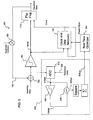
- the high speed receiver 500 illustrated in FIG. 5 includes, by way of example a monitor circuit 505 that tracks the distortion in the soft decision data output by the summer 130 of the decision feedback equalizer.
- the monitor circuit 505 generates a distortion error signal 505(a) from the soft decision data that may be used by a real time optimizer 550 to adjust the phase offset signal of the clock and data recovery circuit 120 to improve the performance of the receiver 500.
- the monitor circuit 505 may include an analog to digital converter 510 that converts the analog soft decision signal output by the summer 130 of the decision feedback equalizer to a digital signal.
- the analog to digital converter samples the analog soft decision at a relatively low rate in response to a low speed reference clock.
- the reference clock 520 may be, for example, a low-frequency signal generated by a stable oscillation source (e.g., a crystal).
- a delay lock loop (not shown) may be used to align the transition edges of the low frequency reference clock 520 with the transition edges of the clock signal which clocks the flip flop 170 of the decision feedback equalizer to ensure that the monitor circuit 505 is properly synchronized with the decision feedback equalizer.
- a delay lock loop which is suitable for synchronizing the reference clock 520 and clock 260 is disclosed in commonly owned U.S. Patent publication US 2005 134 338 entitled. "HIGH FREQUENCY BINARY PHASE DETECTOR", filed December 19, 2003.
- a digital limiter 530 compares the quantized soft decision output by the analog to digital converter 510 with a threshold and generates a binary signal (e.g., one or minus one) having a low value if the quantized signal is less than the threshold and a high value if the quantized signal is greater than or equal to the threshold.
- a combiner 540 generates an error signal 540(a) by subtracting the quantized soft decision 510(a) output by the analog to digital converter with the binary signal 530(a) output by the digital limiter.
- the error signal 540 (a) is squared and then accumulated to generate a sum square error signal.
- a real time optimizer 550 may be used to reduce the value of the sum square error signal as a function of the phase offset of the clock and data recovery circuit 120.
- FIG. 6 is a simplified block diagram of a clock and data recovery circuit 600 that includes a delay 610 coupled between the voltage control oscillator 450 and the phase detector 420 to adjust the phase of the extracted clock signal output by the oscillator 450 to compensate for changes in the delay along the processing path of the decision feedback equalizer of FIG. 1 .
- a real time optimizer 550 may again be used to vary the delay through delay element 610 to reduce the sum square error of the equalized data as previously described with respect to FIG. 5 .
- the integrated decision feedback equalizer and clock and data recovery circuit of the present invention may be integrated into any of a variety of applications.
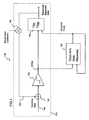
- the described exemplary integrated decision feedback equalizer and clock and data recovery circuit may be incorporated into an optical receiver assembly 710 of an optical communication system 700.
- the optical system 700 includes an optical transmitter 720 and an optical fiber network 730 that carries the optical signal to the optical receiver assembly 710.
- the present invention is not limited to a single optical transmitter and receiver. Rather practical optical communications systems may have one or more optical transmitters as well as one or more optical receivers.
- the illustrated receive path includes an optical detector 735, sensing resistor 740, one or more amplifiers 750, clock and data recovery circuit 760, and decision feedback equalizer 765.
- the optical detector 735 can be any known prior art optical detector. Such prior art detectors convert incoming optical signals into corresponding electrical output signals that can be electronically monitored.
- a transmit path includes, by way of example, one or more gain stage(s) 770 coupled to an optical transmitter 775.
- an analog data source provides an analog data signal that modulates the output of the optical transmitter
- baseband digital modulation or frequency modulation may be used.
- the gain stage(s) amplify the incoming data signal and the amplified data signal in turn drives the optical transmitter 775.
- the gain stage 770 may have multiple stages, and may receive one or more control signals for controlling various different parameters of the output of the optical transmitter.
- the optical transmitter may, for example, be a light emitting diode or a surface emitting laser or an edge emitting laser that operates at high speeds such as 10 Gigabits per second (Gbps) or higher.
- a receive fiber optic cable 730 carries an optical data signal to the optical detector 735.
- a bias voltage applied across the device generates a flow of electric current having an intensity proportional to the intensity of the incident light. In one embodiment, this current flows through sensing resistor 740, and generates a voltage.
- the sensed voltage is amplified by the one or more amplifier(s) 750.
- the output of amplifier 750 drives the decision feedback equalizer 765.
- the decision feedback equalizer includes, by way of example, a slicer that generates a binary signal that drives the clock and data recovery circuit.
- the clock and data recovery circuit generates an extracted clock signal from the binary signal which is coupled to a decision feedback equalizer retimer (as illustrated in FIG. 5 ) to retime the equalized data.
Landscapes
- Engineering & Computer Science (AREA)
- Computer Networks & Wireless Communication (AREA)
- Signal Processing (AREA)
- Physics & Mathematics (AREA)
- Electromagnetism (AREA)
- Power Engineering (AREA)
- Cable Transmission Systems, Equalization Of Radio And Reduction Of Echo (AREA)
- Dc Digital Transmission (AREA)
- Synchronisation In Digital Transmission Systems (AREA)
Claims (9)
- Kommunikationssystem mit:einem entscheidungsrückgekoppelten Entzerrer (110), der so ausgelegt ist, dass er eine kanalbezogene Störung in empfangenen Daten reduziert, wobei der entscheidungsrückgekoppelte Entzerrer (110) entzerrte Daten erzeugt; undeiner Takt- und Datenwiederherstellungsschaltung (120), die an den Entzerrer gekoppelt ist, wobei die Takt- und Datenwiederherstellungsschaltung (120) ein extrahiertes Taktsignal erzeugt, wobei das extrahierte Taktsignal einen einstellbaren Phasenoffset in Bezug auf die entzerrten Daten aufweist, um Verarbeitungsverzögerungen in dem entscheidungsrückgekoppelten Entzerrer (110) auszugleichen, und wobei der entscheidungsrückgekoppelte Entzerrer (110) einen Retimer aufweist, der wiederhergestellte entzerrte Daten aus den entzerrten Daten im Ansprechen auf das extrahierte Taktsignal erzeugt.
- Kommunikationssystem nach Anspruch 1, wobei der entscheidungsrückgekoppelte Entzerrer (110) einen Addierer (130) aufweist, der ein kombiniertes Signal durch Kombinieren eines entzerrten Rückkopplungssignals (150) mit den empfangenen Daten erzeugt, um die kanalbezogene Störung zu reduzieren.
- Kommunikationssystem nach Anspruch 2, wobei der entscheidungsrückgekoppelte Entzerrer (110) des Weiteren einen Slicer (160) aufweist, der an den Addierer (130) gekoppelt ist, wobei der Slicer (160) die entzerrten Daten durch Konvertieren des kombinierten Signals in ein binäres Signal erzeugt, und wobei die Takt- und Datenwiederherstellungsschaltung (120) das extrahierte Taktsignal erzeugt, das einen einstellbaren Phasenoffset in Bezug auf das binäre Signal hat.
- Kommunikationssystem nach Anspruch 3, wobei der Entzerrer-Retimer ein Flip-Flop (170) aufweist, das an den Slicer (160) und die Datenwiederherstellungsschaltung (120) gekoppelt ist, und wobei das Flip-Flop (170) wiederhergestellte entzerrte Daten aus dem binären Signal im Ansprechen auf das extrahierte Taktsignal erzeugt.
- System, das aufweist:einen Sender, der ein Informationssignal über ein Kommunikationsmedium sendet; undeinen Empfänger (500), der an das Kommunikationsmedium gekoppelt ist, um das gesendete Informationssignal zu empfangen, wobei der Empfänger das System der Ansprüche 1 oder 2 enthält.
- Kommunikationssystem nach Anspruch 1, wobei der entscheidungsrückgekoppelte Entzerrer (110) des Weiteren aufweist:einen Addierer (130), der das entzerrte Rückkopplungssignal (150) mit den empfangenen Daten kombiniert,einen Slicer (160), der an den Addierer (130) gekoppelt ist, wobei der Slicer (160) das kombinierte Signal in ein binäres Signal konvertiert; undeinen Multiplizierer (180), der an den Retimer gekoppelt ist;
wobeider Retimer an den Slicer (160) gekoppelt ist und die wiederhergestellten entzerrten Daten aus dem binären Signal im Ansprechen auf das extrahierte Taktsignal erzeugt;der Multiplizierer (180) einen Entzerrungskoeffizienten auf die wiederhergestellten entzerrten Daten anwendet, um das entzerrte Rückkopplungssignal (150) zu erzeugen; unddie Takt- und Datenwiederherstellungsschaltung (120) an den Slicer (160) gekoppelt ist und das extrahierte Taktsignal aus dem binären Signal erzeugt, und die Takt- und Datenwiederherstellungsschaltung (120) die Phase des extrahierten Taktsignals einstellt, um die Verarbeitungsverzögerungen in dem entscheidungsrückgekoppelten Entzerrer (110) auszugleichen. - Kommunikationssystem nach Anspruch 6, wobei die Takt- und Datenwiederherstellungsschaltung (120) aufweist:einen Phasendetektor (420) zum Erzeugen eines Phasenfehlersignals gemäß der Phasendifferenz des extrahierten Taktsignals und des binären Signals;einen spannungsgesteuerten Oszillator (450) zum Erzeugen des extrahierten Taktsignals in Abhängigkeit von dem Phasenfehlersignal; undeine Verzögerung (610), die zwischen den spannungsgesteuerten Oszillator (450) und den Phasendetektor (420) geschaltet ist, um die Phase des extrahierten Taktsignals einzustellen.
- Kommunikationssystem nach Anspruch 1, das des Weiteren aufweist:einen Echtzeit-Optimierer (550), der an die Takt- und Datenwiederherstellungsschaltung (120) gekoppelt ist, wobei der Echtzeit-Optimierer (550) ein Phaseneinstellsignal erzeugt, und wobei die Takt- und Datenwiederherstellungsschaltung (120) die Phase des extrahierten Taktsignals im Ansprechen auf das Phaseneinstellsignal einstellt, um die Verarbeitungsverzögerungen in dem entscheidungsrückgekoppelten Entzerrer (110) auszugleichen.
- Verfahren zum Reduzieren von kanalbezogenen Störungen in empfangenen Daten, das umfasst:Bereitstellen empfangener Daten für einen entscheidungsrückgekoppelten Entzerrer (110);Erzeugen, durch den entscheidungsrückgekoppelten Entzerrer (110), eines binären Signals gemäß den empfangenen Daten;Erzeugen eines Phasenverzögerungssignals, wobei das Phasenverzögerungssignal eine einstellbare Phasenverzögerung zum Ausgleichen der Verarbeitungsverzögerungen in dem entscheidungsrückgekoppelten Entzerrer (110) aufweist;Extrahieren eines Taktsignals aus dem binären Signal gemäß dem Phasenverzögerungssignal; undRetiming des binären Signals gemäß dem Taktsignal.
Applications Claiming Priority (8)
| Application Number | Priority Date | Filing Date | Title |
|---|---|---|---|
| US53096803P | 2003-12-19 | 2003-12-19 | |
| US53140303P | 2003-12-19 | 2003-12-19 | |
| US53140203P | 2003-12-19 | 2003-12-19 | |
| US530968P | 2003-12-19 | ||
| US531403P | 2003-12-19 | ||
| US531402P | 2003-12-19 | ||
| US10/774,725 US7330508B2 (en) | 2003-12-19 | 2004-02-09 | Using clock and data recovery phase adjust to set loop delay of a decision feedback equalizer |
| US774725 | 2004-02-09 |
Publications (3)
| Publication Number | Publication Date |
|---|---|
| EP1545043A2 EP1545043A2 (de) | 2005-06-22 |
| EP1545043A3 EP1545043A3 (de) | 2006-02-22 |
| EP1545043B1 true EP1545043B1 (de) | 2009-04-29 |
Family
ID=34528253
Family Applications (1)
| Application Number | Title | Priority Date | Filing Date |
|---|---|---|---|
| EP04026608A Expired - Lifetime EP1545043B1 (de) | 2003-12-19 | 2004-11-09 | Verwendung von Takt- und Datenrückgewinnungsphase zur Bestimmung der Schleifenverzögerung einer entscheidungsrückgekoppelten Entzerrung |
Country Status (4)
| Country | Link |
|---|---|
| US (1) | US7330508B2 (de) |
| EP (1) | EP1545043B1 (de) |
| CN (1) | CN100496032C (de) |
| DE (1) | DE602004020859D1 (de) |
Families Citing this family (31)
| Publication number | Priority date | Publication date | Assignee | Title |
|---|---|---|---|---|
| US7822113B2 (en) * | 2003-12-19 | 2010-10-26 | Broadcom Corporation | Integrated decision feedback equalizer and clock and data recovery |
| US7623600B2 (en) | 2004-06-02 | 2009-11-24 | Broadcom Corporation | High speed receive equalizer architecture |
| US7167410B2 (en) * | 2005-04-26 | 2007-01-23 | Magnalynx | Memory system and memory device having a serial interface |
| US7702053B2 (en) * | 2005-05-05 | 2010-04-20 | Broadcom Corporation | State based algorithm to minimize mean squared error |
| US7577193B2 (en) * | 2005-06-28 | 2009-08-18 | Intel Corporation | Adaptive equalizer |
| US7599396B2 (en) * | 2005-07-11 | 2009-10-06 | Magnalynx, Inc. | Method of encoding and synchronizing a serial interface |
| US8074126B1 (en) | 2006-06-07 | 2011-12-06 | Marvell International Ltd. | Non-intrusive eye monitor system |
| US7672417B2 (en) * | 2006-08-31 | 2010-03-02 | Montage Technology Group Limited | Clock and data recovery |
| KR100791635B1 (ko) | 2006-09-28 | 2008-01-04 | 고려대학교 산학협력단 | 고속 적응형 이퀄라이저 |
| US7756235B2 (en) * | 2006-09-29 | 2010-07-13 | Agere Systems Inc. | Methods and apparatus for digital compensation of clock errors for a clock and data recovery circuit |
| JP5174493B2 (ja) * | 2008-03-06 | 2013-04-03 | 株式会社日立製作所 | 半導体集積回路装置及びアイ開口マージン評価方法 |
| KR100965767B1 (ko) | 2008-09-08 | 2010-06-24 | 주식회사 하이닉스반도체 | 클럭 복원 회로를 구비하는 결정 피드백 등화기 및 클럭 복원 방법 |
| US8401063B2 (en) | 2008-10-24 | 2013-03-19 | Stmicroelectronics S.R.L. | Decision feedback equalization scheme with minimum correction delay |
| US8249139B2 (en) * | 2009-06-24 | 2012-08-21 | Himax Technologies Limited | Apparatus for data receiving and method for adjusting the same in real time |
| US8181058B2 (en) * | 2010-01-06 | 2012-05-15 | Oracle America, Inc. | Clock-data-recovery technique for high-speed links |
| US8259784B2 (en) * | 2010-03-26 | 2012-09-04 | Realtek Semiconductor Corp. | High-speed continuous-time feedback equalizer for serial link receiver |
| US8737490B1 (en) | 2010-08-20 | 2014-05-27 | Cadence Design Systems, Inc. | Analog-to-digital converter based decision feedback equalization |
| US8737491B1 (en) * | 2010-08-20 | 2014-05-27 | Cadence Design Systems, Inc. | Analog-to-digital converter based decision feedback equalization |
| US8509299B2 (en) | 2011-07-21 | 2013-08-13 | National Semiconductor Corporation | Decision feedback equalizer operable with multiple data rates |
| US9385858B2 (en) * | 2013-02-20 | 2016-07-05 | Avago Technologies General Ip (Singapore) Pte. Ltd. | Timing phase estimation for clock and data recovery |
| US9325489B2 (en) * | 2013-12-19 | 2016-04-26 | Xilinx, Inc. | Data receivers and methods of implementing data receivers in an integrated circuit |
| JP6476659B2 (ja) * | 2014-08-28 | 2019-03-06 | 富士通株式会社 | 信号再生回路および信号再生方法 |
| US9215104B1 (en) * | 2014-09-26 | 2015-12-15 | Intel Corporation | Floating taps for decision feedback equalizer |
| TWI565283B (zh) * | 2014-10-15 | 2017-01-01 | 創意電子股份有限公司 | 時脈資料回復電路與方法 |
| CN106533646B (zh) * | 2015-09-09 | 2019-05-31 | 创意电子股份有限公司 | 序列器/解序列器中的时钟数据恢复系统 |
| CN106301285A (zh) * | 2016-08-03 | 2017-01-04 | 深圳大学 | 基于重定时的固定系数有限冲击响应滤波器结构 |
| US10347283B2 (en) * | 2017-11-02 | 2019-07-09 | Kandou Labs, S.A. | Clock data recovery in multilane data receiver |
| US11231740B2 (en) * | 2019-02-06 | 2022-01-25 | Credo Technology Group Limited | Clock recovery using between-interval timing error estimation |
| US11743080B2 (en) * | 2020-06-29 | 2023-08-29 | Texas Instruments Incorporated | Sample-and-hold-based retimer supporting link training |
| CN112600625B (zh) * | 2020-12-08 | 2022-09-23 | 复旦大学 | 测距通信一体的空间激光外差相干解调处理模块和方法 |
| US11424968B1 (en) * | 2021-06-10 | 2022-08-23 | Credo Technology Group Limited | Retimer training during link speed negotiation and link training |
Family Cites Families (11)
| Publication number | Priority date | Publication date | Assignee | Title |
|---|---|---|---|---|
| DE19510618A1 (de) * | 1994-05-19 | 1995-11-23 | Hammerstein Gmbh C Rob | Kraftfahrzeugsitz, der im vorgeklappten Zustand der Rückenlehne längsverschiebbar ist |
| WO1999038723A1 (en) * | 1998-01-28 | 1999-08-05 | Bertrand Faure Components Ltd. | Rotary recliner control mechanism for multifunction vehicle seat applications |
| US6064272A (en) * | 1998-07-01 | 2000-05-16 | Conexant Systems, Inc. | Phase interpolated fractional-N frequency synthesizer with on-chip tuning |
| JP3946882B2 (ja) * | 1998-09-18 | 2007-07-18 | 富士通株式会社 | 信号処理回路及び信号処理回路の制御方法 |
| US6139104A (en) * | 1999-01-29 | 2000-10-31 | Johnson Controls Technology Company | Multiple function seat back adjusting mechanism |
| US6238002B1 (en) * | 1999-10-08 | 2001-05-29 | Johnson Controls Technology Company | Seat reclining mechanism with integrated seat armrest features |
| JP2001256728A (ja) * | 2000-03-10 | 2001-09-21 | Fujitsu Ltd | 半導体装置 |
| SE517967C2 (sv) * | 2000-03-23 | 2002-08-06 | Ericsson Telefon Ab L M | System och förfarande för klocksignalgenerering |
| JP3532861B2 (ja) * | 2001-02-06 | 2004-05-31 | 松下電器産業株式会社 | Pll回路 |
| US7486894B2 (en) | 2002-06-25 | 2009-02-03 | Finisar Corporation | Transceiver module and integrated circuit with dual eye openers |
| US7184478B2 (en) * | 2003-06-19 | 2007-02-27 | Applied Micro Circuits Corporation | High speed circuits for electronic dispersion compensation |
-
2004
- 2004-02-09 US US10/774,725 patent/US7330508B2/en not_active Expired - Fee Related
- 2004-11-09 EP EP04026608A patent/EP1545043B1/de not_active Expired - Lifetime
- 2004-11-09 DE DE602004020859T patent/DE602004020859D1/de not_active Expired - Lifetime
- 2004-12-17 CN CNB2004101042281A patent/CN100496032C/zh not_active Expired - Fee Related
Also Published As
| Publication number | Publication date |
|---|---|
| CN1638366A (zh) | 2005-07-13 |
| DE602004020859D1 (de) | 2009-06-10 |
| US7330508B2 (en) | 2008-02-12 |
| CN100496032C (zh) | 2009-06-03 |
| EP1545043A2 (de) | 2005-06-22 |
| US20050135470A1 (en) | 2005-06-23 |
| EP1545043A3 (de) | 2006-02-22 |
Similar Documents
| Publication | Publication Date | Title |
|---|---|---|
| EP1545043B1 (de) | Verwendung von Takt- und Datenrückgewinnungsphase zur Bestimmung der Schleifenverzögerung einer entscheidungsrückgekoppelten Entzerrung | |
| EP1545030B1 (de) | Optische Kanalentzerrung | |
| US7623600B2 (en) | High speed receive equalizer architecture | |
| US7961823B2 (en) | System and method for adjusting multiple control loops using common criteria | |
| US7616686B2 (en) | Method and apparatus for generating one or more clock signals for a decision-feedback equalizer using DFE detected data | |
| US7325175B2 (en) | Phase adjust using relative error | |
| US8184686B2 (en) | System and method for recovering data received over a communication channel | |
| US6038266A (en) | Mixed mode adaptive analog receive architecture for data communications | |
| US9294314B2 (en) | Receiver having limiter-enhanced data eye openings | |
| EP1585279A2 (de) | Empfängerschaltkreis mit Entzerrer | |
| US8283982B2 (en) | Decision feedback equalizer circuit | |
| US20050078780A1 (en) | Adaptive equalization system for a signal receiver | |
| US20110274154A1 (en) | Compensated Phase Detector for Generating One or More Clock Signals Using DFE Detected Data in a Receiver | |
| US20060093028A1 (en) | Serial data link using decision feedback equalization | |
| US20050238092A1 (en) | Method and system for error estimation for adaptive equalization in communication systems | |
| US7436882B2 (en) | Decision feedback equalizer and clock and data recovery circuit for high speed applications | |
| EP1545044B1 (de) | Entscheidungsrückgekoppelte Entzerrer und Takt- und Daten-Rückgewinnungsschaltung für Hochgeschwindigkeitsanwendungen | |
| US20050254569A1 (en) | System and method for generating equalization coefficients | |
| US7702053B2 (en) | State based algorithm to minimize mean squared error | |
| US20040032905A1 (en) | Receiver for high rate digital communication system | |
| US7606301B2 (en) | Method and apparatus for adaptively establishing a sampling phase for decision-feedback equalization | |
| US20050249275A1 (en) | Timing recovery method and device for combining pre-filtering and feed-forward equalizing functions | |
| US20050213995A1 (en) | Low power and low jitter optical receiver for fiber optic communication link | |
| US20050135473A1 (en) | Filter with signal taps temporally spaced at fractional symbol intervals | |
| US12407546B2 (en) | Decision-feedback equalizer using feedback filter with controllable delay circuit and associated method |
Legal Events
| Date | Code | Title | Description |
|---|---|---|---|
| PUAI | Public reference made under article 153(3) epc to a published international application that has entered the european phase |
Free format text: ORIGINAL CODE: 0009012 |
|
| AK | Designated contracting states |
Kind code of ref document: A2 Designated state(s): AT BE BG CH CY CZ DE DK EE ES FI FR GB GR HU IE IS IT LI LU MC NL PL PT RO SE SI SK TR |
|
| AX | Request for extension of the european patent |
Extension state: AL HR LT LV MK YU |
|
| PUAL | Search report despatched |
Free format text: ORIGINAL CODE: 0009013 |
|
| AK | Designated contracting states |
Kind code of ref document: A3 Designated state(s): AT BE BG CH CY CZ DE DK EE ES FI FR GB GR HU IE IS IT LI LU MC NL PL PT RO SE SI SK TR |
|
| AX | Request for extension of the european patent |
Extension state: AL HR LT LV MK YU |
|
| 17P | Request for examination filed |
Effective date: 20060822 |
|
| AKX | Designation fees paid |
Designated state(s): DE FR GB |
|
| 17Q | First examination report despatched |
Effective date: 20070309 |
|
| RAP1 | Party data changed (applicant data changed or rights of an application transferred) |
Owner name: BROADCOM CORPORATION |
|
| GRAP | Despatch of communication of intention to grant a patent |
Free format text: ORIGINAL CODE: EPIDOSNIGR1 |
|
| GRAS | Grant fee paid |
Free format text: ORIGINAL CODE: EPIDOSNIGR3 |
|
| GRAA | (expected) grant |
Free format text: ORIGINAL CODE: 0009210 |
|
| AK | Designated contracting states |
Kind code of ref document: B1 Designated state(s): DE FR GB |
|
| REG | Reference to a national code |
Ref country code: GB Ref legal event code: FG4D |
|
| REF | Corresponds to: |
Ref document number: 602004020859 Country of ref document: DE Date of ref document: 20090610 Kind code of ref document: P |
|
| PLBE | No opposition filed within time limit |
Free format text: ORIGINAL CODE: 0009261 |
|
| STAA | Information on the status of an ep patent application or granted ep patent |
Free format text: STATUS: NO OPPOSITION FILED WITHIN TIME LIMIT |
|
| 26N | No opposition filed |
Effective date: 20100201 |
|
| REG | Reference to a national code |
Ref country code: FR Ref legal event code: ST Effective date: 20100730 |
|
| PG25 | Lapsed in a contracting state [announced via postgrant information from national office to epo] |
Ref country code: FR Free format text: LAPSE BECAUSE OF NON-PAYMENT OF DUE FEES Effective date: 20091130 |
|
| PGFP | Annual fee paid to national office [announced via postgrant information from national office to epo] |
Ref country code: GB Payment date: 20161128 Year of fee payment: 13 |
|
| REG | Reference to a national code |
Ref country code: DE Ref legal event code: R082 Ref document number: 602004020859 Country of ref document: DE Representative=s name: BOSCH JEHLE PATENTANWALTSGESELLSCHAFT MBH, DE Ref country code: DE Ref legal event code: R081 Ref document number: 602004020859 Country of ref document: DE Owner name: AVAGO TECHNOLOGIES INTERNATIONAL SALES PTE. LT, SG Free format text: FORMER OWNER: BROADCOM CORP., IRVINE, CALIF., US Ref country code: DE Ref legal event code: R081 Ref document number: 602004020859 Country of ref document: DE Owner name: AVAGO TECHNOLOGIES GENERAL IP (SINGAPORE) PTE., SG Free format text: FORMER OWNER: BROADCOM CORP., IRVINE, CALIF., US |
|
| REG | Reference to a national code |
Ref country code: GB Ref legal event code: 732E Free format text: REGISTERED BETWEEN 20171005 AND 20171011 |
|
| GBPC | Gb: european patent ceased through non-payment of renewal fee |
Effective date: 20171109 |
|
| REG | Reference to a national code |
Ref country code: DE Ref legal event code: R082 Ref document number: 602004020859 Country of ref document: DE Representative=s name: BOSCH JEHLE PATENTANWALTSGESELLSCHAFT MBH, DE Ref country code: DE Ref legal event code: R081 Ref document number: 602004020859 Country of ref document: DE Owner name: AVAGO TECHNOLOGIES INTERNATIONAL SALES PTE. LT, SG Free format text: FORMER OWNER: AVAGO TECHNOLOGIES GENERAL IP (SINGAPORE) PTE. LTD., SINGAPORE, SG |
|
| PG25 | Lapsed in a contracting state [announced via postgrant information from national office to epo] |
Ref country code: GB Free format text: LAPSE BECAUSE OF NON-PAYMENT OF DUE FEES Effective date: 20171109 |
|
| PGFP | Annual fee paid to national office [announced via postgrant information from national office to epo] |
Ref country code: DE Payment date: 20211110 Year of fee payment: 18 |
|
| REG | Reference to a national code |
Ref country code: DE Ref legal event code: R119 Ref document number: 602004020859 Country of ref document: DE |
|
| PG25 | Lapsed in a contracting state [announced via postgrant information from national office to epo] |
Ref country code: DE Free format text: LAPSE BECAUSE OF NON-PAYMENT OF DUE FEES Effective date: 20230601 |