EP1545009A2 - Mehrkanal-Analog-Digital-Wandler, Verfahren und Messgerät mit einem Eingangskanal welcher mit einer vorbestimmten Vorspannung versehen ist - Google Patents
Mehrkanal-Analog-Digital-Wandler, Verfahren und Messgerät mit einem Eingangskanal welcher mit einer vorbestimmten Vorspannung versehen ist Download PDFInfo
- Publication number
- EP1545009A2 EP1545009A2 EP04030033A EP04030033A EP1545009A2 EP 1545009 A2 EP1545009 A2 EP 1545009A2 EP 04030033 A EP04030033 A EP 04030033A EP 04030033 A EP04030033 A EP 04030033A EP 1545009 A2 EP1545009 A2 EP 1545009A2
- Authority
- EP
- European Patent Office
- Prior art keywords
- analog
- input
- digital
- value
- output
- Prior art date
- Legal status (The legal status is an assumption and is not a legal conclusion. Google has not performed a legal analysis and makes no representation as to the accuracy of the status listed.)
- Withdrawn
Links
Images


Classifications
-
- H—ELECTRICITY
- H03—ELECTRONIC CIRCUITRY
- H03M—CODING; DECODING; CODE CONVERSION IN GENERAL
- H03M1/00—Analogue/digital conversion; Digital/analogue conversion
- H03M1/06—Continuously compensating for, or preventing, undesired influence of physical parameters
- H03M1/0617—Continuously compensating for, or preventing, undesired influence of physical parameters characterised by the use of methods or means not specific to a particular type of detrimental influence
- H03M1/0624—Continuously compensating for, or preventing, undesired influence of physical parameters characterised by the use of methods or means not specific to a particular type of detrimental influence by synchronisation
-
- G—PHYSICS
- G06—COMPUTING OR CALCULATING; COUNTING
- G06F—ELECTRIC DIGITAL DATA PROCESSING
- G06F3/00—Input arrangements for transferring data to be processed into a form capable of being handled by the computer; Output arrangements for transferring data from processing unit to output unit, e.g. interface arrangements
- G06F3/05—Digital input using the sampling of an analogue quantity at regular intervals of time, input from a/d converter or output to d/a converter
-
- H—ELECTRICITY
- H03—ELECTRONIC CIRCUITRY
- H03M—CODING; DECODING; CODE CONVERSION IN GENERAL
- H03M3/00—Conversion of analogue values to or from differential modulation
- H03M3/30—Delta-sigma modulation
- H03M3/322—Continuously compensating for, or preventing, undesired influence of physical parameters
- H03M3/324—Continuously compensating for, or preventing, undesired influence of physical parameters characterised by means or methods for compensating or preventing more than one type of error at a time, e.g. by synchronisation or using a ratiometric arrangement
-
- H—ELECTRICITY
- H03—ELECTRONIC CIRCUITRY
- H03M—CODING; DECODING; CODE CONVERSION IN GENERAL
- H03M1/00—Analogue/digital conversion; Digital/analogue conversion
- H03M1/12—Analogue/digital converters
- H03M1/1205—Multiplexed conversion systems
- H03M1/122—Shared using a single converter or a part thereof for multiple channels, e.g. a residue amplifier for multiple stages
- H03M1/1225—Shared using a single converter or a part thereof for multiple channels, e.g. a residue amplifier for multiple stages using time-division multiplexing
-
- H—ELECTRICITY
- H03—ELECTRONIC CIRCUITRY
- H03M—CODING; DECODING; CODE CONVERSION IN GENERAL
- H03M3/00—Conversion of analogue values to or from differential modulation
- H03M3/30—Delta-sigma modulation
- H03M3/458—Analogue/digital converters using delta-sigma modulation as an intermediate step
- H03M3/466—Multiplexed conversion systems
- H03M3/472—Shared, i.e. using a single converter for multiple channels
- H03M3/474—Shared, i.e. using a single converter for multiple channels using time-division multiplexing
Definitions
- the invention relates to analog-to-digital converters and, more particularly, to meters employing analog-to-digital converters for a plurality of alternating current power lines.
- the invention also relates to a method of analog-to-digital conversion and, more particularly, to such a method that synchronizes serially communicated output digital values from analog-to-digital conversions.
- a typical mechanism for resolving this issue is to employ dedicated hardware to provide a suitable synchronization signal. For example, if the starting point of a clock associated with one set of serial data for the different channels of an analog-to-digital (A/D) converter is known; then the dedicated hardware can be employed to assure synchronization (and, thus, provide a subsequent starting point) for a subsequent second set of data for those different channels. However, in the absence of such a synchronization signal, another mechanism is required.
- Channel synchronization can apply to any count of plural channels.
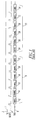
- Figure 1 shows, for six channels, the relative timing of serial data including a serial enable (SE) input signal 2, a serial data output frame sync (SDOFS) output signal 4, and a serial data output (SDO) signal 6 from a six-channel, serial output A/D converter (not shown) for two successive sets 8,10 of six samples.
- Serial data is normally read from the A/D converter with simultaneously sampled channels appearing in consecutive order (i.e., samples 12,14,16,18,20,22 of the first set 8; samples 24,26,28,30,32,34 of the second set 10). This process is continuous until the sampling system of the A/D converter is reset or loses power.
- some A/D converters output one SDOFS output signal for only the first of six samples.
- the present invention introduces a unique direct current offset to one input channel, such as, for example, to one of the alternating current waveforms input by a plurality of input channels of a serial output analog-to-digital (A/D) converter.
- A/D analog-to-digital
- an analog-to-digital converter apparatus comprises: a plurality of first input channels, each of the first input channels including an alternating current signal having a direct current value of about zero; a second input channel having a predetermined direct current bias value, which is different than zero; means for biasing and scaling each of the first and second input channels and providing a plurality of analog outputs; means for providing a plurality of analog to digital conversions for each of the analog outputs and outputting a plurality of digital values; means for serially communicating the digital values for a first set of the analog to digital conversions before serially communicating the digital values for a subsequent second set of the analog to digital conversions without providing any synchronization of the digital values for both of the first and second sets of the analog to digital conversions; and means for serially receiving the serially communicated digital values and saving the same.
- the second input channel may include a predetermined direct current voltage.
- the second input channel may include an alternating current signal having a direct current value of about zero, and the second input channel may be biased by a predetermined direct current value, which is different than zero.
- a method of analog-to-digital conversion comprises: employing a plurality of first input channels, each of the first input channels including an alternating current signal having a direct current value of about zero; employing a second input channel having a predetermined direct current bias value, which is different than zero; biasing and scaling each of the first input channels and providing a plurality of analog outputs; providing a plurality of analog to digital conversions for each of the analog outputs and the second input channel and outputting a plurality of output digital values; serially communicating the output digital values for a first set of the analog to digital conversions before serially communicating the output digital values for a subsequent second set of the analog to digital conversions without providing any synchronization of the digital values for both of the first and second sets of the analog to digital conversions; serially receiving the serially communicated output digital values and storing corresponding input digital values for each of the first and second input channels; and processing the input digital values.
- the method may further comprise averaging the input digital values for each of the first and second input channels; and identifying from the averaged input digital values one or more of the first and second input channels having a direct current offset value, which is greater than a predetermined value.
- the method may further comprise inputting a plurality of alternating current line signals at the first input channels; employing a line cycle with the line signals; selecting a time period corresponding to an integer count of the line cycle; and averaging the input digital values over the time period.
- the method may further comprise determining whether one or more of the first input channels has a direct current offset value, which is greater than the predetermined value.
- the method may further comprise determining that the second input channel has a direct current offset value, which is less than the predetermined value; determining that only one of the first input channels has the direct current offset value, which is greater than the predetermined value; and responsively rearranging the input digital values for the first input channels for the time period.
- the method may further comprise determining that none of the first input channels has the direct current offset value, which is greater than the predetermined value; determining that the second input channel has a direct current offset value, which is greater than the predetermined value; and employing the input digital values for the first input channels for the time period.
- the method may further comprise determining that more than one of the first input channels has the direct current offset value, which is greater than the predetermined value; and responsively discarding the input digital values for the first input channels for the time period.
- a meter for a plurality of power lines comprises: a plurality of first input channels, each of the first input channels including an alternating current signal having a direct current value of about zero, the first input channels include a plurality of alternating current line voltage signals and a plurality of alternating current line current signals; a second input channel having an analog output with a predetermined direct current bias value, which is different than zero; a plurality of biasing and scaling circuits each of which inputs a corresponding one of the alternating current line voltage signals and the alternating current line current signals, and outputs a corresponding analog output; a plurality of analog to digital converters each of which inputs a corresponding one of the analog outputs of the biasing and scaling circuits and the second input channel and outputs a corresponding digital value; a serial output circuit serially communicating the corresponding digital values for a first set of analog to digital conversions before serially communicating the digital values for a subsequent second set of the analog to digital conversions without providing any synchronization of the first input channels
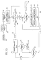
- the system 42 includes a plurality of first input channels 44 and a second input channel 46.
- the first input channels 44 include alternating current signals having a direct current value of about zero.
- the second input channel 46 has a predetermined direct current bias value, which is different than zero.
- the first input channels 44 include a plurality of alternating current (e.g. , 50 Hz; 60 Hz; 400 Hz) line voltage (e.g., 110 VAC; 220 VAC; 480 VAC; 600 VAC) signals V A 48, V B 50, V C 52 and 53.
- the signals 48,50,52 are from a three-phase AC power source (not shown).
- the second input channel 46 includes an alternating current line voltage signal V N 54, which, for example, corresponds to a neutral line (not shown) of the AC power source.
- the system 42 also includes a plurality of analog bias and scaling circuits 56,58,60,61 for biasing and scaling the signals 48,50,52,53 and providing corresponding analog outputs 62,64,66,67, respectively.
- the system 42 further includes an analog bias and scaling circuit 68 for biasing and scaling the signal 54 and providing a corresponding analog output 70.
- the alternating current line voltage signal V N 54 has a direct current value of about zero
- the second input channel 46 is biased by a predetermined direct current bias value, such as predetermined direct current voltage VDC 72, which is different than zero ( e.g ., a suitable percentage of the full scale range of the analog outputs 62,64,66,67,70).
- the A/D converter 40 includes a plurality of analog inputs 74,76,78,80,82 for the respective analog outputs 62,64,66,67,70, and a serial data output (SDO) 84.
- SDO serial data output
- the A/D converter 40 functions to provide a plurality of analog to digital conversions for each of the analog outputs 62,64,66,67,70 and to provide a plurality of corresponding digital values 83.
- the A/D converter 40 functions to serially communicate those digital values 83 from the serial data output 84 for a first set of the analog to digital conversions before serially communicating the digital values for a subsequent second set of the analog to digital conversions, without providing any synchronization of the digital values 83 for both of the first and second sets of the analog to digital conversions.
- the serial data output 84 includes a serial data stream 86, which provides no synchronization of the sequential sets of the digital values 83 for the first and second input channels 44,46.
- the system 42 further includes a suitable circuit, such as, for example, a processor (e.g ., digital signal processor (DSP) 88), which serially receives the serially communicated digital values 83 from the serial data stream 86 and saves the same.
- DSP digital signal processor
- the DSP 88 includes a serial port 90, a direct memory access (DMA) controller 92, a memory 94 and a processor 96.
- the serial port 90 includes an input 98, which serially receives the serially communicated digital values 83 from the serial data output 84.
- the serial port 90 converts the serial data stream 86 to a sequence of digital values 99, which are transferred by the DMA controller 92 for storage in the memory 94 as input digital values (in an array 267) for subsequent processing by the processor 96. In this manner, the serial port 90 and the DMA controller 92 move streams of serial data into the memory 94.
- DSP 88 any suitable processor and/or digital circuit may be employed for serially receiving and manipulating the serial data stream 86.
- the A/D digital values 83 in the serial data stream 86 are from the plural A/D channels (not shown) of the A/D converter 40. These values 83 stream through the single serial port 90, in order that the data from all channels 44,46 is in consecutive memory locations in the memory array 267.
- DC offset keying By employing DC offset keying with the single second channel 46, it is possible to determine if the data samples for the first channels 44 are in their intended locations in the memory array 267. Furthermore, as will be discussed below in connection with Figures 12A and 12B, because the data is in consecutive memory locations, a detected shift in the data samples may readily be corrected.
- Figure 3 shows an example of a six channel serial output A/D converter 40' including five first input channels 100 and a second input channel 102.
- the A/D converter 40' in this example is a model AD73360L six-input channel analog front end marketed by Analog Devices of Norwood, Massachusetts.
- the first input channels 100 include a plurality of alternating current line current signals I A 104, I B 106, I C 108 and I N 110, and an alternating current line voltage signal V A 112.
- These alternating current line current signals 104 and 106,108,110 correspond, for example, to the alternating current line voltage signal 112 and the alternating current line voltage signals 50,52,54 of Figure 2, respectively.
- the second input channel 102 includes an alternating current line current signal I G 114, which corresponds to a ground line (not shown) of a three-phase AC power source (not shown).
- the signal I G 114 has a direct current value of about zero.
- a plurality of analog bias and scaling circuits 116,118,120,122,124,126 for biasing and scaling the analog input signals 112,104,106,108,110,114 and providing corresponding analog outputs 128,130,132,134,136,138, respectively.
- analog outputs 128,130,132,134,136,138 are input by respective analog inputs 140,142,144,146,148,150 of the A/D converter 40'.
- the circuit 116 is similar to the circuit 152 of Figure 4.
- the circuits 118,120,122,124 are similar to the circuit 154 of Figure 8.
- the circuit 126 is similar to the circuit 156 of Figure 9.
- that circuit 126 biases the second input channel 102 with a predetermined direct current bias value, which is different than zero. That bias value is determined by a reference voltage 202 from a buffer amplifier 205, and by resistors 230,238.
- the AD73360L A/D converter 40' is a six-input channel, 16-bit, analog front end including six independent encoder channels corresponding to the six analog inputs 140,142,144,146,148,150. As shown following the analog input 140, each of these channels includes a signal conditioner 158, a switched capacitor programmable gain amplifier (PGA) 160, a sigma-delta analog-to-digital (A/D) converter (ADC) 162 and a decimator 164. An on-board digital filter (not shown), which forms part of the sigma-delta ADC 162, also performs critical system-level filtering. Each of the ADCs, such as 162, corresponds to one of the alternating current signals of the first and second input channels 100,102.
- a serial I/O port 166 receives digital values from the decimators, such as 164, and provides a suitable interface 167 to a processor (not shown) and/or another cascaded A/D converter (not shown).
- the interface 167 includes a RESET input 168, which receives an active low reset signal, in order to reset the entire A/D converter 40' including control registers (not shown) and other digital circuitry (not shown).
- a MCLK input 170 receives a master clock input from a suitable external clock signal source (not shown).
- a SCLK output 172 provides an output serial clock, which has a rate that determines the serial transfer rate to/from the serial I/O port 166.
- the frequency of the SCLK output 172 is equal to the frequency of the master clock MCLK input 170 divided by an integer number, which is the product of an external master clock rate divider (not shown) and a serial clock rate divider (not shown).
- the SE input 174 is an asynchronous input enable for the serial I/O port 166.
- the SE input 174 is set low, the outputs of the port 166 are three-stated and the inputs thereof are ignored.
- the SE input 174 is set high, the control and data registers (not shown) of the port 166 are at their original values.
- the SDOFS output 176 provides the framing signal output for serial transfers on the SDO output 178.
- the signal of the SDOFS output 176 is one bit wide and is active one SCLK period before the first bit (i.e., most significant bit in the example) of each output word.
- the SDO output 178 provides a serial data output for data (e.g., a serial stream of digital values) and control information to be output and clocked on the positive edge of the signal on the SCLK output 172 when the signal on the SE input 174 is set high.
- data e.g., a serial stream of digital values
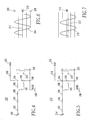
- the analog bias and scaling circuit 152 is for a power system alternating current line voltage input, V IN 180, such as the input signals 48,50,52,53 of Figure 2 or the input signal 112 of Figure 3.
- the circuit 152 includes a divider 181 formed by resistors 182,184,186,188,190 and an output 192 defined by nodes 194 and 196.
- the node 196 is electrically connected to a suitable analog ground AGND 198.
- the circuit 152 suitably reduces the alternating current voltage of the corresponding alternating current line voltage input 180.
- Another resistor 200 is electrically connected between the divider node 194 and the direct current reference voltage, Vref 202, which biases the differential output 192 to be at least zero volts.
- the output 192 may include a filter capacitor 203, as shown.
- the incoming AC waveforms of the input signals 48,50,52,53 of Figure 2 or the input signal 112 of Figure 3 have no inherent DC offset, in order that any long-term DC offset is assumed to be a measurement error. This is true for the AC voltage of the voltage input V IN 180, which is measured through the voltage divider, 181, and for the AC current of the current input I IN 203 of the circuit 154 of Figure 8.
- the signal 204 of the output 192 of Figure 5 has a sinusoidal waveform, which ranges between a peak full scale (FS) value 206 and a minimum value (0) 208.
- the average value of the signal 204 is preferably selected by the circuit 152 ( Figure 5) to provide a mid scale (MS) value 210 of the corresponding A/D converter, such as 40 or 40'.
- MS mid scale
- the minimum value (0) 208 is 0000H
- the mid scale (MS) value 210 is 7FFFH
- the peak full scale (FS) value 206 is FFFFH.
- the signal 204' of the output 192' of the circuit 154 has a sinusoidal waveform, which ranges between a peak full scale (FS) value 206' and a minimum value (0) 208'.
- the average value of the signal 204' is preferably selected by the circuit 154 to provide a mid scale (MS) value 210' of the corresponding A/D converter, such as 40'.
- Figure 5 shows an analog bias and scaling circuit 212 for a power system alternating current line voltage input, V N 214, such as the input alternating current line voltage signal V N 54 of Figure 2 for a neutral line of an AC power source (not shown).
- the circuit 212 is structurally very similar to the circuit 152 of Figure 4, with one exception.
- the resistors 190,200 have about the same resistance values, in order that the signal 204 ( Figure 6) from the output 192 has an average value 211, which is about equal to the mid scale (MS) value 210.
- the resistors 190,216 have different resistance values ( e .
- the resistance of the resistor 216 is suitably greater than the resistance of resistor 190), in order that the signal 218 ( Figure 7) from the output 220 has an average value, which is suitably less than the mid scale (MS) value 210.
- MS mid scale
- the (MS) value 210 is 7FFFH
- the average value 222 is about 45% of the peak full scale (FS) value 206, FFFFH of Figure 6, or about 7332H in this example.
- the divider output 220 is biased to be a predetermined DC voltage.
- relatively low-amplitude AC signals are employed in the synchronization channel through an intentional DC offset.
- a signal having zero AC signal is most preferred, since it provides a DC measure that is independent of time.
- a DC offset having a relatively small AC signal will not approach the minimum or maximum values of the A/D converter numbering system (e.g., where, for example, for a 16-bit system, 7FFFH is the mid scale (MS) value, which is defined to be zero). Since, for example, V N 54 ( Figure 2) and I G 114 ( Figure 3) are usually about zero, each is an example of a preferred synchronization channel.
- the DC measure over an integer number of cycles is determined by a frequency measurement at step 256 ( Figure 12A). If the frequency measurement is in error or delayed, then the DC component could be off by a significant amount.
- the peak to peak value of the signal 204 may be at or about the peak full scale (FS) value 206, while the peak to peak value of the signal 218 ( Figure 7) is typically much less than the peak full scale (FS) value 206.
- the average value of the signal 204 is essentially the MS value 210 or is essentially 50% of the FS value 206, while the average value of the signal 218 is intentionally biased to be different from the MS value 210 (e.g., about 45% of the FS value 206). Although 45% is disclosed, any suitable percentage (e.g., without limitation, 25%; 40%; 48%; 49%; 51%; 52%; 60%; 75%) or offset above or below the MS value 210 may be employed.
- the analog bias and scaling circuit 154 is for a power system alternating current line current input, I IN 203, such as the input signals 104,106,108,110 of Figure 3.
- the circuit 154 includes a current transformer 224 having a primary winding 226, a secondary winding 228 and a burden resistor 230.
- the terminals 232,234 of the burden resistor 230 are electrically connected in parallel with the secondary winding 228.
- the second terminal 234 is biased by a direct current reference voltage, Vref 202', which may be the same as the reference voltage, Vref 202 of Figures 4 and 5.
- the reference voltage 202' biases the signal 204' ( Figure 10) of the output 192' of the circuit 154, in order that the average value of the signal 204' is the mid scale (MS) value 210' ( Figure 10) of the corresponding A/D converter (not shown).
- the output 192' may include a filter capacitor 235, as shown.
- Figure 9 shows the analog bias and scaling circuit 156 for the power system alternating current line current input, I G 236, such as the input signal 114 of Figure 3.
- the circuit 156 is structurally very similar to the circuit 154 of Figure 8, with one exception.
- the first terminal 232 of the burden resistor 230 is electrically connected by a resistor 238 to an analog ground 198', which may be the same as the analog ground 198 of Figures 4 and 5.
- the resistors 238,230 have different resistance values (e.g., the resistance of the resistor 238 is suitably greater (e.g., 10 times) than the resistance of resistor 230), in order that the signal 240 ( Figure 11) from the output 242 has an average value, which is suitably less than the mid scale (MS) value 210'.
- MS mid scale
- the (MS) value 210' is 7FFFH
- the average value 244 is about 45% of the peak full scale (FS) value 206', FFFFH of Figure 10, or about 7332H in this example.
- the circuit output 242 is biased to be a predetermined DC voltage.
- the peak to peak value of the signal 204' may be at or about the peak full scale (FS) value 206' of Figure 10, while the peak to peak value of the signal 240 is typically much less than the peak full scale (FS) value 206'.
- the average value of the signal 204' of Figure 10 is essentially the MS value 210' or essentially 50% of the FS value 206', while the average value of the signal 240 of Figure 11 of the output 242 is intentionally biased to be different from the MS value 210' (e.g., about 45% of the FS value 206' of Figure 10). Although 45% is disclosed, any suitable percentage ( e.g ., without limitation, 25%; 40%; 48%; 49%; 51%; 52%; 60%; 75%) or offset above or below the MS value 210' may be employed.
- the respective bias resistors 216 and 238 introduce suitable DC offset voltages.
- a DC offset may be introduced to either an unused A/D channel or to an A/D channel that is not operatively associated with one of the three power-line phases.
- the offset is introduced to V N 214 of Figure 5, V NG (not shown) or I G 236 of Figure 9 rather than the phase voltage signals V A 48, V B 50, V C 52, V AN (not shown), V BN (not shown) or V CN (not shown), or the phase current signals I A 104, I B 106, I C 108 or IN 110 of Figures 2 and 3.
- Figures 12A and 12B show a SyncProcess routine 250 executed by the processor 96 of Figure 2, although this routine is applicable to any of the A/D converter systems disclosed herein.
- the routine 250 starts, at 252, and initializes three variables, Sample, ChanSum [] (for each channel) and ERROR, to zero, and variable "i" to one at 254.
- the Line Frequency associated with the alternating current signals such as the line voltage signals 48,50,52 of Figure 2 is determined.
- a predetermined frequency value from memory 94 may be employed.
- the average cycle time of the alternating current signals may be suitably determined and inverted, in order to obtain the average frequency value.
- a preferably integer count of cycles in a predetermined measurement period is determined based upon the Line Frequency. For example, if the predetermined measurement period is selected to be 200 ms, then the integer count of line cycles (CyclesPer200ms) would be 10 line cycles at 50 Hz or 12 line cycles at 60 Hz.
- the precision is not critical. However, for other purposes, accurate removal of the DC component may be desirable.
- the average value of the corresponding AC data is accumulated over the period of an integer number of line cycles.
- the data is accumulated over the period of 200 ms to account for both 50 Hz and 60 Hz applications ( e.g ., 10 and 12 cycles, respectively).
- variable j is set equal to zero.
- the variable j which was initialized to zero at step 261, is between 0 and one less than the count of channels, NumChan (e.g., 6 as shown in Figure 3; any suitable channel count). If not, then the variable, Sample; is incremented, at 264, before step 260 is repeated.
- the variable SerialADCval is determined from a StoredSample array 267 in the memory 94 of Figure 2.
- the StoredSample array 267 is indexed, at 266, by i*Sample + j.
- step 262 If there are samples for more than one measurement period in the memory array 267 (e.g., a circular buffer), then "i" is suitably controlled outside of the routine 250, in order to point to the corresponding measurement period of interest. Alternatively, the variable “i” need not be employed if samples from only one measurement period are in the memory array 267.
- the variable SerialADCval is added to an intermediate channel sum value, ChanSum[j], for the current channel of interest, j. Then, at 270, the variable j is incremented before step 262 is repeated.
- step 274 determines the average value, ChanAvg[j] for the current channel of interest, j, based upon the final channel sum value, ChanSum[j], from step 268, divided by the count of samples, Sample, from step 264.
- step 276 it is determined if the ChanAvg[j] for the current channel is greater than a predetermined threshold value (e.g ., without limitation, 5% of the full scale (FS) value). If so, then a flag for the current channel of interest, Flag[j], is set true at 278.
- a predetermined threshold value e.g ., without limitation, 5% of the full scale (FS) value
- Step 276 identifies all channels having at least a predetermined DC offset. In practice, all non-intentional DC offsets are effectively cancelled by suitable calibration settings in the A/D converter 40, in order that the net DC offset on all channels is about zero. If, however, the samples for the different channels are shifted, then the purposefully offset synchronization channel 46 of Figure 2 and at least one other channel will have a significant DC offset (e.g., about 5%FS or greater) as detected at step 276.
- a significant DC offset e.g., about 5%FS or greater
- a count, NumOffsetChan, of the channels having a significant DC offset is determined based upon a count (e.g., zero, one or more) of the flags, Flag[], which are true.
- NumOffsetChan is equal to one and if the Flag[] for the channel having the intentional DC offset (e.g ., Flag[5] for channel 102 of Figure 3, wherein 0 [j [ 5 for that six-channel system) is true. If so, since this is the normally expected situation, the variables OffsetSam and Error are reset to zero at 288 and 290, respectively.
- NumOffsetChan is equal to one and if the Flag[] for the channel having the intentional DC offset is false (or if any one of the other Flag[] variables is true).
- the variable OffsetSam is set equal to the variable FlaggedChan (e.g ., the value of j such that Flag[j] is true) less the variable SyncChan ( e.g ., 5 for channel 102 of Figure 3). Then, at 296, the variable Error is reset to zero.
- the array 267 of Figure 2 normally contains the following sequence of channel data: "0,1,2,3,4,5,6,7,8,9,10,11,0,1,2,3,4,5,6,7,8,9,10,11,".
- the channel #5 is the synchronization channel (i.e., having the normally expected DC offset)
- channel #2 is the channel with the detected DC offset
- the channel sampling is off by three sample times.
- the correct channel data is indexed by i*Sample + j + OffsetSam.
- NumOffsetChan i.e., the count of channels, including the SyncChan, having an offset
- the last measurement period e.g. 200 ms.
- a non-recoverable sampling error has occurred within the last measurement period.
- all data in the StoredSample array 267 in the memory 94 for that period is responsively discarded at 300.
- the variable Error is incremented.
- the processor 96 of Figure 2 employs all of the digital values in the array 267 for the first input channels 44 for the previous time period ( e.g ., 200 ms).
- the processor 96 restarts the A/D digital conversions, the A/D converter 40 ( Figure 2) serially communicates the output digital values on output 84 for a subsequent set of the A/D conversions, the DSP 88 serially receives the serially communicated output digital values through the serial port 90, and the DMA controller 92 stores the corresponding input digital values 99 in the memory 94 for each of the first and second input channels (e.g., 44 and 46 of Figure 2).
- one or two of the single AD73360L A/D converter 40' of Figure 3 may be employed to measure the voltages and currents in all phases of a plural-phase power supply (not shown).
- the simultaneous sampling architecture of the converter 40' is ideal for this application where simultaneous sampling is critical to maintaining the relative phase information between the plural voltage and current phases.
- two or more A/D channels may be employed to measure the voltages in each phase via the circuit 152 of Figure 4.
- Two or more A/D channels may be employed to measure the current flowing in each phase via the circuit 154 of Figure 8.
- any suitable current-sensing isolation amplifiers and/or Hall-effect sensors may be employed.
- a suitable processor such as the DSP 88 of Figure 2 is employed to perform the mathematical calculations on the digital values provided by the A/D converter 40'.
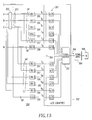
- Figure 13 shows an example meter 350 including an A/D converter 352 having 12 channels 354 for a three-phase power line 353.
- the channels 354 input three phase voltages V A , V B , V C , one neutral voltage V N , three phase currents I A , I B , I C , one neutral current I N , one ground current I G , and three additional phase voltages V AG , V BC , V CG , which are referenced, for example, on the primary side of a transformer (T) 355. All of the channels 354 are associated with alternating current signals having a direct current value of about zero.
- All but one or two of these channels 354 are part of first channels 44', which employ biasing and scaling circuits (BSCs) 356,357, which input a corresponding one of the alternating current line voltage signals and the alternating current line current signals, and which output a corresponding analog output.
- BSCs biasing and scaling circuits
- one (or both) of the neutral voltage V N and the ground current I G are associated with a second channel 46' and biasing and scaling circuits (BSCBs) 358,359 employing a predetermined direct current bias value, which is different than zero.
- the A/D converter 352 employs a plurality of analog-to-digital (A/D) converters 360 each of which inputs a corresponding one of the analog outputs of the biasing and scaling circuits 356,357,358,359 and outputs a corresponding digital value.
- the A/D converter 352 includes a serial output circuit 362 serially communicating the corresponding digital values for a first set of analog to digital conversions before serially communicating the digital values for a subsequent second set of the analog to digital conversions without providing any synchronization of the corresponding digital values for both of the first and second sets of the analog to digital conversions.
- a suitable serial input circuit 364 serially receives the serially communicated digital values 366 and saves the same in a memory (M) 368.
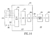
- Figure 14 shows another plural channel serial output A/D converter 370 and system 372.
- the A/D converter 370 includes a single analog-to-digital (A/D) converter 374 having an analog multiplexer 376 with a plurality of analog inputs 378, with each of the analog inputs 378 corresponding to one of the first and second input channels 380,382.
- the channel 382 includes an alternating current signal having a DC offset.
- a serial output (SO) circuit 384 outputs the digital values 366 to the serial input circuit 364.
Landscapes
- Engineering & Computer Science (AREA)
- Theoretical Computer Science (AREA)
- Human Computer Interaction (AREA)
- Physics & Mathematics (AREA)
- General Engineering & Computer Science (AREA)
- General Physics & Mathematics (AREA)
- Analogue/Digital Conversion (AREA)
Applications Claiming Priority (2)
| Application Number | Priority Date | Filing Date | Title |
|---|---|---|---|
| US10/740,130 US6906655B1 (en) | 2003-12-18 | 2003-12-18 | Plural channel analog-to-digital converter, method and meter employing an input channel with a predetermined direct current bias |
| US740130 | 2003-12-18 |
Publications (2)
| Publication Number | Publication Date |
|---|---|
| EP1545009A2 true EP1545009A2 (de) | 2005-06-22 |
| EP1545009A3 EP1545009A3 (de) | 2005-08-17 |
Family
ID=34523206
Family Applications (1)
| Application Number | Title | Priority Date | Filing Date |
|---|---|---|---|
| EP04030033A Withdrawn EP1545009A3 (de) | 2003-12-18 | 2004-12-17 | Mehrkanal-Analog-Digital-Wandler, Verfahren und Messgerät mit einem Eingangskanal welcher mit einer vorbestimmten Vorspannung versehen ist |
Country Status (4)
| Country | Link |
|---|---|
| US (1) | US6906655B1 (de) |
| EP (1) | EP1545009A3 (de) |
| CA (1) | CA2490304C (de) |
| ZA (1) | ZA200410164B (de) |
Cited By (2)
| Publication number | Priority date | Publication date | Assignee | Title |
|---|---|---|---|---|
| DE102007001221A1 (de) * | 2007-01-05 | 2008-07-10 | Texas Instruments Deutschland Gmbh | Mehrphasen-Elektroenergiezähler |
| WO2008081047A3 (en) * | 2007-01-05 | 2008-10-09 | Texas Instruments Deutschland | Poly-phase electric energy meter |
Families Citing this family (13)
| Publication number | Priority date | Publication date | Assignee | Title |
|---|---|---|---|---|
| JP4248998B2 (ja) * | 2003-11-18 | 2009-04-02 | ナイルス株式会社 | エンコーダ |
| US7705756B2 (en) * | 2006-11-03 | 2010-04-27 | Slicex, Inc. | Multi-channel analog-to-digital converter |
| US7400283B1 (en) * | 2006-12-19 | 2008-07-15 | Actel Corporation | Mixed signal system-on-a-chip integrated simultaneous multiple sample/hold circuits and embedded analog comparators |
| US8194789B2 (en) * | 2007-12-05 | 2012-06-05 | Hunt Technologies, Llc | Input signal combiner system and method |
| JP5327085B2 (ja) * | 2010-02-01 | 2013-10-30 | 株式会社デンソー | A/d変換処理装置 |
| US9479188B1 (en) * | 2010-05-28 | 2016-10-25 | Maxim Integrated Products, Inc. | Programmable multichannel signal selector |
| KR101133352B1 (ko) * | 2010-12-22 | 2012-04-19 | 한국전력공사 | 전자식 전력량계 및 전력량 계산 방법 |
| JP2012146268A (ja) * | 2011-01-14 | 2012-08-02 | Kyocera Corp | 携帯電子機器、制御方法及び制御プログラム |
| US9063178B2 (en) * | 2011-07-27 | 2015-06-23 | Eaton Corporation | System for measuring current and method of making same |
| EP3217560A1 (de) * | 2016-03-11 | 2017-09-13 | Socionext Inc. | Analog/digital-umsetzung |
| WO2019020357A1 (de) * | 2017-07-26 | 2019-01-31 | Tridonic Gmbh & Co Kg | Schaltungsanordnung und verfahren zur ermittlung eines einen stromistwert repräsentierenden signals |
| EP3527996B1 (de) * | 2018-02-19 | 2023-03-29 | Siemens Aktiengesellschaft | Messanordnung und verfahren zum messen elektrischer signale |
| US12562930B2 (en) * | 2022-11-18 | 2026-02-24 | The United States Of America As Represented By The Secretary Of The Navy | Sensor system |
Family Cites Families (5)
| Publication number | Priority date | Publication date | Assignee | Title |
|---|---|---|---|---|
| US4656585A (en) * | 1984-02-03 | 1987-04-07 | Sundstrand Data Control Inc. | Aircraft flight data recorder data acquisition system |
| JPS62217988A (ja) * | 1986-03-19 | 1987-09-25 | 双葉電子工業株式会社 | 模型飛行機等無線遠隔操縦装置におけるチヤンネル変更装置 |
| US5099239A (en) * | 1989-09-21 | 1992-03-24 | Xerox Corporation | Multi-channel analogue to digital convertor |
| SE500357C2 (sv) * | 1992-01-31 | 1994-06-06 | Silicon Construction Sweden Ab | Arrangemang för analog/digital-omvandling |
| JP3911386B2 (ja) * | 2000-12-12 | 2007-05-09 | 富士通テン株式会社 | Dma通信制御方法、転送データ処理方法、dma通信制御装置、及びエンジン制御装置 |
-
2003
- 2003-12-18 US US10/740,130 patent/US6906655B1/en not_active Expired - Lifetime
-
2004
- 2004-12-15 ZA ZA200410164A patent/ZA200410164B/xx unknown
- 2004-12-15 CA CA2490304A patent/CA2490304C/en not_active Expired - Fee Related
- 2004-12-17 EP EP04030033A patent/EP1545009A3/de not_active Withdrawn
Cited By (6)
| Publication number | Priority date | Publication date | Assignee | Title |
|---|---|---|---|---|
| DE102007001221A1 (de) * | 2007-01-05 | 2008-07-10 | Texas Instruments Deutschland Gmbh | Mehrphasen-Elektroenergiezähler |
| WO2008081047A3 (en) * | 2007-01-05 | 2008-10-09 | Texas Instruments Deutschland | Poly-phase electric energy meter |
| WO2008081046A3 (en) * | 2007-01-05 | 2008-10-30 | Texas Instruments Deutschland | Polyphase electric energy meter |
| US7589516B2 (en) | 2007-01-05 | 2009-09-15 | Texas Instruments Incorporated | Poly-phase electric energy meter |
| US7689374B2 (en) | 2007-01-05 | 2010-03-30 | Texas Instruments Deutschland Gmbh | Polyphase electric energy meter |
| DE102007001221B4 (de) * | 2007-01-05 | 2011-09-22 | Texas Instruments Deutschland Gmbh | Mehrphasen-Elektroenergiezähler |
Also Published As
| Publication number | Publication date |
|---|---|
| EP1545009A3 (de) | 2005-08-17 |
| ZA200410164B (en) | 2005-07-19 |
| US6906655B1 (en) | 2005-06-14 |
| CA2490304A1 (en) | 2005-06-18 |
| US20050134490A1 (en) | 2005-06-23 |
| CA2490304C (en) | 2013-01-22 |
Similar Documents
| Publication | Publication Date | Title |
|---|---|---|
| US6906655B1 (en) | Plural channel analog-to-digital converter, method and meter employing an input channel with a predetermined direct current bias | |
| US7652602B2 (en) | Signal interface circuit | |
| US6243034B1 (en) | Integrating analog to digital converter with improved resolution | |
| US7106233B2 (en) | Integrated galvanomagnetic sensor array system | |
| EP1875611B1 (de) | Auswählbare abtastauslösung in echtzeit für mehrere eingänge eines analog-digital-wandlers | |
| US7768253B2 (en) | Sampling module and a method of sampling one or more analogue characteristics of a power transmission system | |
| EP0104999B1 (de) | Vorrichtung zur Umschaltung der Verstärkung mit vermindertem Fehler für ein Wattmeter | |
| US4907165A (en) | Electric energy measuring method | |
| EP0551503A1 (de) | Integrierender analog-digitalumsetzer mit mittel zur reduzierung von "rolloverfehler" | |
| US5373292A (en) | Integration type D-A/A-D Conversion apparatus capable of shortening conversion processing time | |
| JPH10232250A (ja) | rmsコンバータ、rms値測定装置、およびrms値計算方法 | |
| US8280655B2 (en) | Digital power monitoring circuit and system | |
| JP2003179493A (ja) | データ取得装置 | |
| DK166750B1 (da) | Fremgangsmaade til bestemmelse af vaerdier af analoge spaendinger, som optraeder paa abonnenttilslutningsledninger i et fortrinsvis digitalt telefonformidlingssystem, og en kobling til udoevelse af fremgangsmaaden | |
| US20020027454A1 (en) | Multi-channel precision synchronous voltage-to-frequency converter | |
| JPS62115857A (ja) | 半導体集積回路装置 | |
| RU2097777C1 (ru) | Многоканальный преобразователь сигналов резистивных датчиков во временной интервал | |
| GB2227381A (en) | Analogue to digital converters | |
| RU2195767C1 (ru) | Устройство для преобразования напряжения переменного тока в код | |
| SU1046928A1 (ru) | Цифровой вольтметр | |
| SU1272263A1 (ru) | Устройство дл измерени посто нного тока | |
| JPS632488B2 (de) | ||
| RU2060586C1 (ru) | Преобразователь напряжения в интервал времени | |
| CN116481599A (zh) | 多通道信号采集设备和传感器系统 | |
| SU1449845A1 (ru) | Многоканальное измерительное устройство дл дифференциальных индуктивных датчиков |
Legal Events
| Date | Code | Title | Description |
|---|---|---|---|
| PUAI | Public reference made under article 153(3) epc to a published international application that has entered the european phase |
Free format text: ORIGINAL CODE: 0009012 |
|
| AK | Designated contracting states |
Kind code of ref document: A2 Designated state(s): AT BE BG CH CY CZ DE DK EE ES FI FR GB GR HU IE IS IT LI LT LU MC NL PL PT RO SE SI SK TR |
|
| AX | Request for extension of the european patent |
Extension state: AL BA HR LV MK YU |
|
| PUAL | Search report despatched |
Free format text: ORIGINAL CODE: 0009013 |
|
| AK | Designated contracting states |
Kind code of ref document: A3 Designated state(s): AT BE BG CH CY CZ DE DK EE ES FI FR GB GR HU IE IS IT LI LT LU MC NL PL PT RO SE SI SK TR |
|
| AX | Request for extension of the european patent |
Extension state: AL BA HR LV MK YU |
|
| 17P | Request for examination filed |
Effective date: 20060207 |
|
| AKX | Designation fees paid |
Designated state(s): ES FR GB |
|
| REG | Reference to a national code |
Ref country code: DE Ref legal event code: 8566 |
|
| 17Q | First examination report despatched |
Effective date: 20061018 |
|
| GRAP | Despatch of communication of intention to grant a patent |
Free format text: ORIGINAL CODE: EPIDOSNIGR1 |
|
| INTG | Intention to grant announced |
Effective date: 20130408 |
|
| RAP1 | Party data changed (applicant data changed or rights of an application transferred) |
Owner name: EATON CORPORATION |
|
| STAA | Information on the status of an ep patent application or granted ep patent |
Free format text: STATUS: THE APPLICATION IS DEEMED TO BE WITHDRAWN |
|
| 18D | Application deemed to be withdrawn |
Effective date: 20130820 |