EP1544906A1 - Verfahren und einrichtung zur laserstrahlverarbeitung eines siliziumsubstrats und verfahren und einrichtung zum laserstrahlschneiden einer siliziumverdrahtung - Google Patents
Verfahren und einrichtung zur laserstrahlverarbeitung eines siliziumsubstrats und verfahren und einrichtung zum laserstrahlschneiden einer siliziumverdrahtung Download PDFInfo
- Publication number
- EP1544906A1 EP1544906A1 EP03771391A EP03771391A EP1544906A1 EP 1544906 A1 EP1544906 A1 EP 1544906A1 EP 03771391 A EP03771391 A EP 03771391A EP 03771391 A EP03771391 A EP 03771391A EP 1544906 A1 EP1544906 A1 EP 1544906A1
- Authority
- EP
- European Patent Office
- Prior art keywords
- silicon
- laser
- silicon substrate
- micron
- laser beam
- Prior art date
- Legal status (The legal status is an assumption and is not a legal conclusion. Google has not performed a legal analysis and makes no representation as to the accuracy of the status listed.)
- Withdrawn
Links
Images


Classifications
-
- H—ELECTRICITY
- H10—SEMICONDUCTOR DEVICES; ELECTRIC SOLID-STATE DEVICES NOT OTHERWISE PROVIDED FOR
- H10D—INORGANIC ELECTRIC SEMICONDUCTOR DEVICES
- H10D84/00—Integrated devices formed in or on semiconductor substrates that comprise only semiconducting layers, e.g. on Si wafers or on GaAs-on-Si wafers
- H10D84/201—Integrated devices formed in or on semiconductor substrates that comprise only semiconducting layers, e.g. on Si wafers or on GaAs-on-Si wafers characterised by the integration of only components covered by H10D1/00 or H10D8/00, e.g. RLC circuits
- H10D84/204—Integrated devices formed in or on semiconductor substrates that comprise only semiconducting layers, e.g. on Si wafers or on GaAs-on-Si wafers characterised by the integration of only components covered by H10D1/00 or H10D8/00, e.g. RLC circuits of combinations of diodes or capacitors or resistors
- H10D84/212—Integrated devices formed in or on semiconductor substrates that comprise only semiconducting layers, e.g. on Si wafers or on GaAs-on-Si wafers characterised by the integration of only components covered by H10D1/00 or H10D8/00, e.g. RLC circuits of combinations of diodes or capacitors or resistors of only capacitors
-
- B—PERFORMING OPERATIONS; TRANSPORTING
- B23—MACHINE TOOLS; METAL-WORKING NOT OTHERWISE PROVIDED FOR
- B23K—SOLDERING OR UNSOLDERING; WELDING; CLADDING OR PLATING BY SOLDERING OR WELDING; CUTTING BY APPLYING HEAT LOCALLY, e.g. FLAME CUTTING; WORKING BY LASER BEAM
- B23K26/00—Working by laser beam, e.g. welding, cutting or boring
- B23K26/36—Removing material
- B23K26/40—Removing material taking account of the properties of the material involved
-
- B—PERFORMING OPERATIONS; TRANSPORTING
- B23—MACHINE TOOLS; METAL-WORKING NOT OTHERWISE PROVIDED FOR
- B23K—SOLDERING OR UNSOLDERING; WELDING; CLADDING OR PLATING BY SOLDERING OR WELDING; CUTTING BY APPLYING HEAT LOCALLY, e.g. FLAME CUTTING; WORKING BY LASER BEAM
- B23K26/00—Working by laser beam, e.g. welding, cutting or boring
- B23K26/60—Preliminary treatment
-
- H—ELECTRICITY
- H10—SEMICONDUCTOR DEVICES; ELECTRIC SOLID-STATE DEVICES NOT OTHERWISE PROVIDED FOR
- H10D—INORGANIC ELECTRIC SEMICONDUCTOR DEVICES
- H10D84/00—Integrated devices formed in or on semiconductor substrates that comprise only semiconducting layers, e.g. on Si wafers or on GaAs-on-Si wafers
- H10D84/201—Integrated devices formed in or on semiconductor substrates that comprise only semiconducting layers, e.g. on Si wafers or on GaAs-on-Si wafers characterised by the integration of only components covered by H10D1/00 or H10D8/00, e.g. RLC circuits
- H10D84/204—Integrated devices formed in or on semiconductor substrates that comprise only semiconducting layers, e.g. on Si wafers or on GaAs-on-Si wafers characterised by the integration of only components covered by H10D1/00 or H10D8/00, e.g. RLC circuits of combinations of diodes or capacitors or resistors
- H10D84/209—Integrated devices formed in or on semiconductor substrates that comprise only semiconducting layers, e.g. on Si wafers or on GaAs-on-Si wafers characterised by the integration of only components covered by H10D1/00 or H10D8/00, e.g. RLC circuits of combinations of diodes or capacitors or resistors of only resistors
-
- H—ELECTRICITY
- H10—SEMICONDUCTOR DEVICES; ELECTRIC SOLID-STATE DEVICES NOT OTHERWISE PROVIDED FOR
- H10W—GENERIC PACKAGES, INTERCONNECTIONS, CONNECTORS OR OTHER CONSTRUCTIONAL DETAILS OF DEVICES COVERED BY CLASS H10
- H10W20/00—Interconnections in chips, wafers or substrates
- H10W20/01—Manufacture or treatment
- H10W20/031—Manufacture or treatment of conductive parts of the interconnections
- H10W20/067—Manufacture or treatment of conductive parts of the interconnections by modifying the pattern of conductive parts
- H10W20/068—Manufacture or treatment of conductive parts of the interconnections by modifying the pattern of conductive parts by using a laser, e.g. laser cutting or laser direct writing
-
- H—ELECTRICITY
- H10—SEMICONDUCTOR DEVICES; ELECTRIC SOLID-STATE DEVICES NOT OTHERWISE PROVIDED FOR
- H10W—GENERIC PACKAGES, INTERCONNECTIONS, CONNECTORS OR OTHER CONSTRUCTIONAL DETAILS OF DEVICES COVERED BY CLASS H10
- H10W20/00—Interconnections in chips, wafers or substrates
- H10W20/40—Interconnections external to wafers or substrates, e.g. back-end-of-line [BEOL] metallisations or vias connecting to gate electrodes
- H10W20/49—Adaptable interconnections, e.g. fuses or antifuses
- H10W20/493—Fuses, i.e. interconnections changeable from conductive to non-conductive
- H10W20/494—Fuses, i.e. interconnections changeable from conductive to non-conductive changeable by the use of an external beam, e.g. laser beam or ion beam
-
- B—PERFORMING OPERATIONS; TRANSPORTING
- B23—MACHINE TOOLS; METAL-WORKING NOT OTHERWISE PROVIDED FOR
- B23K—SOLDERING OR UNSOLDERING; WELDING; CLADDING OR PLATING BY SOLDERING OR WELDING; CUTTING BY APPLYING HEAT LOCALLY, e.g. FLAME CUTTING; WORKING BY LASER BEAM
- B23K2101/00—Articles made by soldering, welding or cutting
- B23K2101/36—Electric or electronic devices
- B23K2101/40—Semiconductor devices
-
- B—PERFORMING OPERATIONS; TRANSPORTING
- B23—MACHINE TOOLS; METAL-WORKING NOT OTHERWISE PROVIDED FOR
- B23K—SOLDERING OR UNSOLDERING; WELDING; CLADDING OR PLATING BY SOLDERING OR WELDING; CUTTING BY APPLYING HEAT LOCALLY, e.g. FLAME CUTTING; WORKING BY LASER BEAM
- B23K2103/00—Materials to be soldered, welded or cut
- B23K2103/50—Inorganic materials other than metals or composite materials
Definitions
- the present invention relates to a laser processing method and device for the same, wherein splattering of molten silicon does not take place during laser processing of silicon substrates used in semiconductor devices.
- a system made from semiconductor devices may use tens of thousands to hundreds of thousands of parts such as transistors and diodes. If a malfunction in even one of these parts were to render the system inoperable, it would not be possible to provide increased reliability and redundancy. Therefore, devices can have built-in means for correcting problems in the entire device caused by malfunctions in individual parts by providing ahead of time multiple redundant circuits with short-circuit sections. This makes it possible to cut off and remove a section where a malfunction took place.
- Fig. 1 is a simplified drawing of an example of an electronic circuit in which fine adjustments to device performances can be made.
- Fig. 1 (a) shows an electronic circuit in which fine adjustments can be made to capacitance.
- Fig. 1 (b) shows an electronic circuit in which fine adjustments can be made to resistance.
- a capacitor 2-1 and capacitors 2-2 - 2-5 are connected in parallel, and short-circuit sections 3-2 - 3-5 are disposed at the wiring for the capacitors 2-2 - 2-5.
- opening some or all of the short-circuit sections 3-2 - 3-5 allows fine adjustments of the overall capacitance of the electronic circuit 1a to be made.
- a resistor 4-1 and resistors 4-2 - 4-5 are connected in series, and the resistors 4-2 - 4-5 are connected in parallel to short-circuit sections 5-2 - 5-5.
- a laser with a high energy density is applied because of the need to melt and vaporize the silicon substrate.
- a beam with an energy density of approximately 110,000 J/m 2 must generally be applied.
- Fig. 2 illustrates the formation of a hole in a mirror surface of a silicon substrate using a laser.
- Fig. 2 (a) is a simplified cross-section drawing showing the state of the silicon surface when processing takes place.
- Fig. 2 (b) shows the energy distribution of the laser.
- Fig. 2 (c) shows the distribution of the effective energy of the laser.
- Fig. 2 (a) when applying a laser beam 7 to the surface of a silicon substrate 6-1 to form a hole, the silicon substrate 6-1 melts and spatters, creating spatterings 6-2. When these spatterings 6-2 are created, they can obstruct the insulation properties of the semiconductor devices and can adhese to nearby parts and lead to malfunctions. As a result, the reliability of the device is significantly decreased.
- the present inventor investigated the causes of the spatterings 6-2 shown in Fig. 2 (a) and observed the following.
- the energy density of the laser 7 applied to the perimeter area of the hole is low from the start.
- the effective energy is low and the silicon substrate 6-1 is liquefied rather than being vaporized.
- the liquefied silicon around the perimeter area of the hole is spattered around the hole by the pressure from the vaporized silicon near the center.
- the present inventor performed similar tests with the position with the highest laser energy density shifted away from the center of the hole toward the perimeter area. It was found that silicon spattered most on the side opposite from the direction in which the position with the highest energy density was shifted. This occurred because the perimeter area on the side away from the direction of the shift of the highest energy density position had more liquefied silicon than the perimeter area of the hole on the side toward the direction of the shift.
- the object of the present invention is to provide a laser processing method and device for the same that prevents spattering of melted silicon, that provides superior processing precision, and that allows efficient hole-forming and cutting of a silicon substrate.
- the present invention essentially provides a silicon substrate laser processing method described in (1) below and a laser processing device described in (2) below. This processing method and processing device are especially useful in cutting silicon wiring.
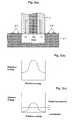
- Fig. 3 illustrates the forming of a hole in silicon according to the method of the present invention.
- Fig. 3 (a) is a simplified cross-section drawing showing the surface of the silicon when the process is being performed.
- Fig. 3 (b) shows the distribution of laser energy.
- Fig. 3 (c) shows the distribution of effective energy from the laser.
- a laser 7 is applied to silicon on the surface of which are formed projections and indentations to provide a predetermined roughness.
- the hole can be formed without the creation of the spatterings 6-2 formed in Fig. 2 (a) described above. This is because the laser 7 applied to the rough silicon surface undergoes irregular reflection and is absorbed into the silicon more easily.
- Fig. 3 (c) while the effective energy of the laser 7 is less than the applied energy, a high level can be maintained overall. As a result, silicon is vaporized not only near the center of the hole but also at the perimeter section, so that the spattering of silicon can be prevented.
- the present inventors performed various studies based on the above observations, and based on the results, completed the laser processing method of the present invention, in which projections and indentations of 0.05 micron - 1 micron Ra are formed on the surface of the silicon substrate and a laser is applied.
- the lower limit of the Ra of the silicon substrate surface is set to 0.05 microns.
- the lower limit is preferably 0.1 micron.
- the upper limit of the Ra of the silicon substrate surface is set to 1 micron.
- the upper limit is preferably 0.5 micron.
- the roughness (Ra) of the silicon substrate surface is adjusted to 0.05 micron - 1 micron, and then a laser is applied.
- This laser processing method is especially useful when cutting silicon wiring.
- Means for adjusting the silicon substrate surface roughness (Ra) to 0.05 micron - 1 micron can include, for example, (1) through (5) below.
- a resist is applied to a silicon substrate on which an oxide film is formed.
- the substrate is then developed and rinsed, after which dry etching or wet etching is performed.
- a mask opening is formed on the silicon substrate, and C 3 F 8 or C 4 F 8 plasma is used to form a deposition film on the opening that is non-uniform over a very fine level. This is then exposed to SF 8 plasma. As a result, isotropic etching is begun from the sections with a thinner deposition film, and etching takes place starting from the sections where the deposition film has been removed. Indentations and projections can be formed to a predetermined roughness on the silicon substrate surface by adjusting the diameter of the mask opening, the plasma exposure time, the chamber pressure, the electrical power applied to the substrate, and the like.
- a focused silicon ion beam is applied in a localized manner to an oxide film formed on the silicon substrate. Patterning is performed on the oxide film by removing the sections on exposed to the ion beam using 2.5% HF. Then, the oxide film is used as a mask to perform anisotropic etching using hydrazine. Since the sections of the oxide film exposed to the ion beam have a greater etching rate in response to HF, indentations and projections can be formed to a predetermined roughness on the silicon substrate surface by adjusting the conditions of the focused silicon ion beam applied to the oxide film (e.g., acceleration voltage, exposure time).
- the conditions of the focused silicon ion beam applied to the oxide film e.g., acceleration voltage, exposure time.
- an in-feed grinder is used with wafer rotation to perform surface grinding of a silicon wafer with a diamond wheel.
- Indentations and projections can be formed to a predetermined roughness on the silicon substrate surface by adjusting spindle speed, grinding time, the count of the diamond wheel, and the like.
- This method is an application of the pigment discharge method using in inkjet printers. More specifically, inkjet printers print onto paper by discharging a fast-drying solvent such as MEK (methyl ethyl ketone) in which an inorganic pigment such as carbon black is dispersed. Indentations and projections can be formed to a predetermined roughness on the silicon substrate surface by adjusting the particle diameter of the sprayed pigment within a predetermined range.
- a fast-drying solvent such as MEK (methyl ethyl ketone) in which an inorganic pigment such as carbon black is dispersed.
- Indentations and projections can be formed to a predetermined roughness on the silicon substrate surface by adjusting the particle diameter of the sprayed pigment within a predetermined range.
- the laser beam can be applied with a solid-state laser (light source: ruby, YAG (yttrium-aluminum-garnet), glass, alexandrite, or the like), a gas laser (light source: CO 2 , CO, Ar ion, or the like), an excimer laser (light source: Ar F, Kr F, XeCl, Xe F, or the like), a metal vapor laser (light source: Cu ion or the like), a dye laser (e.g., a Dye laser), or the like, but it would be preferable to use a YAG laser or a CO 2 laser because of the high output that can be obtained.
- a solid-state laser light source: ruby, YAG (yttrium-aluminum-garnet), glass, alexandrite, or the like
- a gas laser light source: CO 2 , CO, Ar ion, or the like
- an excimer laser light source: Ar F, Kr F, Xe
- a YAG laser and a nonlinear crystal can be used to form a hole with a diameter of approximately 15 microns and a depth of approximately 40 microns.
- a laser can be applied under the conditions described below. As described above, if these conditions are met, good processing efficiency can be maintained, and spattering of melted silicon does not take place even at the laser energy densities used.
- the present invention makes it possible to prevent spattering of melted silicon.
Landscapes
- Engineering & Computer Science (AREA)
- Physics & Mathematics (AREA)
- Optics & Photonics (AREA)
- Plasma & Fusion (AREA)
- Mechanical Engineering (AREA)
- Laser Beam Processing (AREA)
- Internal Circuitry In Semiconductor Integrated Circuit Devices (AREA)
Applications Claiming Priority (3)
| Application Number | Priority Date | Filing Date | Title |
|---|---|---|---|
| JP2002220036 | 2002-07-29 | ||
| JP2002220036 | 2002-07-29 | ||
| PCT/JP2003/009557 WO2004012253A1 (ja) | 2002-07-29 | 2003-07-28 | シリコン基板のレーザ処理方法およびその装置、ならびにシリコン配線のレーザ切断方法およびその装置 |
Publications (2)
| Publication Number | Publication Date |
|---|---|
| EP1544906A1 true EP1544906A1 (de) | 2005-06-22 |
| EP1544906A4 EP1544906A4 (de) | 2008-08-13 |
Family
ID=31184749
Family Applications (1)
| Application Number | Title | Priority Date | Filing Date |
|---|---|---|---|
| EP03771391A Withdrawn EP1544906A4 (de) | 2002-07-29 | 2003-07-28 | Verfahren und einrichtung zur laserstrahlverarbeitung eines siliziumsubstrats und verfahren und einrichtung zum laserstrahlschneiden einer siliziumverdrahtung |
Country Status (3)
| Country | Link |
|---|---|
| EP (1) | EP1544906A4 (de) |
| AU (1) | AU2003252278A1 (de) |
| WO (1) | WO2004012253A1 (de) |
Family Cites Families (5)
| Publication number | Priority date | Publication date | Assignee | Title |
|---|---|---|---|---|
| JPS58170037A (ja) * | 1982-03-31 | 1983-10-06 | Toshiba Corp | 配線の切断方法及び切断装置 |
| JPH08191038A (ja) * | 1995-01-11 | 1996-07-23 | Kawasaki Steel Corp | 半導体基板へのマーキング方法 |
| JPH09270400A (ja) * | 1996-01-31 | 1997-10-14 | Shin Etsu Handotai Co Ltd | 半導体ウェーハの製造方法 |
| DE10012840C2 (de) * | 2000-03-16 | 2001-08-02 | Wacker Siltronic Halbleitermat | Verfahren zur Herstellung einer Vielzahl von polierten Halbleiterscheiben |
| JP2003045828A (ja) * | 2001-08-01 | 2003-02-14 | Sony Corp | 半導体処理方法および処理装置 |
-
2003
- 2003-07-28 AU AU2003252278A patent/AU2003252278A1/en not_active Abandoned
- 2003-07-28 EP EP03771391A patent/EP1544906A4/de not_active Withdrawn
- 2003-07-28 WO PCT/JP2003/009557 patent/WO2004012253A1/ja not_active Ceased
Also Published As
| Publication number | Publication date |
|---|---|
| AU2003252278A1 (en) | 2004-02-16 |
| WO2004012253A1 (ja) | 2004-02-05 |
| EP1544906A4 (de) | 2008-08-13 |
Similar Documents
| Publication | Publication Date | Title |
|---|---|---|
| US6720522B2 (en) | Apparatus and method for laser beam machining, and method for manufacturing semiconductor devices using laser beam machining | |
| US4826785A (en) | Metallic fuse with optically absorptive layer | |
| US10741399B2 (en) | Femtosecond laser-induced formation of submicrometer spikes on a semiconductor substrate | |
| US4935801A (en) | Metallic fuse with optically absorptive layer | |
| JP3660294B2 (ja) | 半導体装置の製造方法 | |
| CN102007653B (zh) | 以修整的激光脉冲用于激光钻孔之方法与装置 | |
| KR100456931B1 (ko) | 투영마스크제조방법 | |
| JP2597818B2 (ja) | マイクロフューズの削除方法 | |
| CN102388438B (zh) | 用于处理基板的方法、用于生产半导体芯片的方法和用于生产具有树脂粘结剂层的半导体芯片的方法 | |
| US4877480A (en) | Lithographic technique using laser for fabrication of electronic components and the like | |
| CN1330580A (zh) | 激光处理 | |
| JP6095320B2 (ja) | 液体吐出ヘッド用基板の製造方法 | |
| EP2266134B1 (de) | Verarbeiten von mehrschichtigen halbleiterwafern | |
| JP2006032419A (ja) | ウエーハのレーザー加工方法 | |
| DE102020101520B4 (de) | Halbleitervorrichtung und verfahren | |
| EP0256938B1 (de) | Lithographisches Verfahren unter Anwendung von Laser zur Herstellung von elektronischen Elementen und ähnlichen | |
| US20050150877A1 (en) | Method and device for laser beam processing of silicon substrate, and method and device for laser beam cutting of silicon wiring | |
| US5288664A (en) | Method of forming wiring of semiconductor device | |
| EP1544906A1 (de) | Verfahren und einrichtung zur laserstrahlverarbeitung eines siliziumsubstrats und verfahren und einrichtung zum laserstrahlschneiden einer siliziumverdrahtung | |
| JP2002337347A (ja) | 液体吐出ヘッドおよびその製造方法 | |
| EP1800791A1 (de) | Verfahren zur Schaffung eines Kontaktloches mit Hilfe eines Laserstrahls | |
| JP3998974B2 (ja) | 回路基板のパターニング方法 | |
| JP2004074279A (ja) | シリコン基板のレーザ処理方法およびその装置、ならびにシリコン配線のレーザ切断方法およびその装置 | |
| JP4422528B2 (ja) | 荷電粒子線用転写マスクの製造方法 | |
| JP2008085118A (ja) | 半導体装置の製造方法 |
Legal Events
| Date | Code | Title | Description |
|---|---|---|---|
| PUAI | Public reference made under article 153(3) epc to a published international application that has entered the european phase |
Free format text: ORIGINAL CODE: 0009012 |
|
| 17P | Request for examination filed |
Effective date: 20050228 |
|
| AK | Designated contracting states |
Kind code of ref document: A1 Designated state(s): AT BE BG CH CY CZ DE DK EE ES FI FR GB GR HU IE IT LI LU MC NL PT RO SE SI SK TR |
|
| AX | Request for extension of the european patent |
Extension state: AL LT LV MK |
|
| DAX | Request for extension of the european patent (deleted) | ||
| RBV | Designated contracting states (corrected) |
Designated state(s): DE GB |
|
| A4 | Supplementary search report drawn up and despatched |
Effective date: 20080711 |
|
| STAA | Information on the status of an ep patent application or granted ep patent |
Free format text: STATUS: THE APPLICATION HAS BEEN WITHDRAWN |
|
| 17Q | First examination report despatched |
Effective date: 20081002 |
|
| 18W | Application withdrawn |
Effective date: 20081002 |