EP1544668A1 - Method of sealing an array of cell microstructures using microencapsulated adhesive - Google Patents
Method of sealing an array of cell microstructures using microencapsulated adhesive Download PDFInfo
- Publication number
- EP1544668A1 EP1544668A1 EP20040029259 EP04029259A EP1544668A1 EP 1544668 A1 EP1544668 A1 EP 1544668A1 EP 20040029259 EP20040029259 EP 20040029259 EP 04029259 A EP04029259 A EP 04029259A EP 1544668 A1 EP1544668 A1 EP 1544668A1
- Authority
- EP
- European Patent Office
- Prior art keywords
- substrate
- microcapsules
- end portion
- adhesive
- wall microstructure
- Prior art date
- Legal status (The legal status is an assumption and is not a legal conclusion. Google has not performed a legal analysis and makes no representation as to the accuracy of the status listed.)
- Withdrawn
Links
- 239000000853 adhesive Substances 0.000 title claims abstract description 81
- 230000001070 adhesive effect Effects 0.000 title claims abstract description 81
- 238000000034 method Methods 0.000 title claims abstract description 41
- 238000007789 sealing Methods 0.000 title claims abstract description 13
- 239000000758 substrate Substances 0.000 claims abstract description 125
- 239000003094 microcapsule Substances 0.000 claims abstract description 98
- 239000000126 substance Substances 0.000 claims abstract description 43
- 238000000576 coating method Methods 0.000 claims description 45
- 239000007788 liquid Substances 0.000 claims description 36
- 239000011248 coating agent Substances 0.000 claims description 29
- 239000002245 particle Substances 0.000 claims description 19
- 239000004824 Multi-part adhesive Substances 0.000 claims description 12
- 239000000843 powder Substances 0.000 claims description 11
- GWEVSGVZZGPLCZ-UHFFFAOYSA-N Titan oxide Chemical compound O=[Ti]=O GWEVSGVZZGPLCZ-UHFFFAOYSA-N 0.000 claims description 6
- 239000011521 glass Substances 0.000 claims description 6
- 239000013060 biological fluid Substances 0.000 claims description 5
- 239000011859 microparticle Substances 0.000 claims description 5
- 239000004973 liquid crystal related substance Substances 0.000 claims description 4
- 239000000314 lubricant Substances 0.000 claims description 4
- 239000002304 perfume Substances 0.000 claims description 4
- 238000003618 dip coating Methods 0.000 claims description 3
- 238000004070 electrodeposition Methods 0.000 claims description 3
- 238000007788 roughening Methods 0.000 claims description 3
- 238000007650 screen-printing Methods 0.000 claims description 3
- 238000004528 spin coating Methods 0.000 claims description 3
- 238000005507 spraying Methods 0.000 claims description 3
- 238000010345 tape casting Methods 0.000 claims description 3
- 238000012546 transfer Methods 0.000 claims description 3
- 238000013019 agitation Methods 0.000 claims description 2
- 238000000151 deposition Methods 0.000 claims description 2
- 238000005530 etching Methods 0.000 claims description 2
- 238000007761 roller coating Methods 0.000 claims description 2
- 238000003825 pressing Methods 0.000 claims 1
- 210000004027 cell Anatomy 0.000 description 30
- 239000000463 material Substances 0.000 description 11
- 239000002103 nanocoating Substances 0.000 description 9
- 238000010276 construction Methods 0.000 description 8
- 239000010410 layer Substances 0.000 description 8
- BLRPTPMANUNPDV-UHFFFAOYSA-N Silane Chemical compound [SiH4] BLRPTPMANUNPDV-UHFFFAOYSA-N 0.000 description 7
- 229910000077 silane Inorganic materials 0.000 description 7
- 239000012790 adhesive layer Substances 0.000 description 6
- 230000008569 process Effects 0.000 description 6
- 230000009471 action Effects 0.000 description 4
- 230000003287 optical effect Effects 0.000 description 4
- 101100386510 Mus musculus Dazap2 gene Proteins 0.000 description 3
- 210000002421 cell wall Anatomy 0.000 description 3
- NBVXSUQYWXRMNV-UHFFFAOYSA-N fluoromethane Chemical compound FC NBVXSUQYWXRMNV-UHFFFAOYSA-N 0.000 description 3
- 150000002484 inorganic compounds Chemical class 0.000 description 3
- 229910010272 inorganic material Inorganic materials 0.000 description 3
- 230000005855 radiation Effects 0.000 description 3
- 239000004593 Epoxy Substances 0.000 description 2
- 238000003491 array Methods 0.000 description 2
- 230000006835 compression Effects 0.000 description 2
- 238000007906 compression Methods 0.000 description 2
- 238000004049 embossing Methods 0.000 description 2
- PCHJSUWPFVWCPO-UHFFFAOYSA-N gold Chemical compound [Au] PCHJSUWPFVWCPO-UHFFFAOYSA-N 0.000 description 2
- 229910052737 gold Inorganic materials 0.000 description 2
- 239000010931 gold Substances 0.000 description 2
- FFUAGWLWBBFQJT-UHFFFAOYSA-N hexamethyldisilazane Chemical compound C[Si](C)(C)N[Si](C)(C)C FFUAGWLWBBFQJT-UHFFFAOYSA-N 0.000 description 2
- 239000007769 metal material Substances 0.000 description 2
- 239000000203 mixture Substances 0.000 description 2
- 238000000206 photolithography Methods 0.000 description 2
- 150000004756 silanes Chemical class 0.000 description 2
- 239000002356 single layer Substances 0.000 description 2
- WYTZZXDRDKSJID-UHFFFAOYSA-N (3-aminopropyl)triethoxysilane Chemical compound CCO[Si](OCC)(OCC)CCCN WYTZZXDRDKSJID-UHFFFAOYSA-N 0.000 description 1
- 108010010803 Gelatin Proteins 0.000 description 1
- BQCADISMDOOEFD-UHFFFAOYSA-N Silver Chemical compound [Ag] BQCADISMDOOEFD-UHFFFAOYSA-N 0.000 description 1
- 238000010521 absorption reaction Methods 0.000 description 1
- XAGFODPZIPBFFR-UHFFFAOYSA-N aluminium Chemical compound [Al] XAGFODPZIPBFFR-UHFFFAOYSA-N 0.000 description 1
- 229910052782 aluminium Inorganic materials 0.000 description 1
- 238000013459 approach Methods 0.000 description 1
- 230000009286 beneficial effect Effects 0.000 description 1
- 230000008901 benefit Effects 0.000 description 1
- 230000000975 bioactive effect Effects 0.000 description 1
- 238000007664 blowing Methods 0.000 description 1
- 239000002775 capsule Substances 0.000 description 1
- 150000001875 compounds Chemical class 0.000 description 1
- 239000007822 coupling agent Substances 0.000 description 1
- 238000011161 development Methods 0.000 description 1
- 238000006073 displacement reaction Methods 0.000 description 1
- 230000000694 effects Effects 0.000 description 1
- 239000012530 fluid Substances 0.000 description 1
- 229920002313 fluoropolymer Polymers 0.000 description 1
- 229920000159 gelatin Polymers 0.000 description 1
- 239000008273 gelatin Substances 0.000 description 1
- 235000019322 gelatine Nutrition 0.000 description 1
- 235000011852 gelatine desserts Nutrition 0.000 description 1
- 238000007496 glass forming Methods 0.000 description 1
- 239000003292 glue Substances 0.000 description 1
- 230000005484 gravity Effects 0.000 description 1
- 230000001788 irregular Effects 0.000 description 1
- 230000002427 irreversible effect Effects 0.000 description 1
- 238000004519 manufacturing process Methods 0.000 description 1
- 239000008204 material by function Substances 0.000 description 1
- 238000001053 micromoulding Methods 0.000 description 1
- 230000005012 migration Effects 0.000 description 1
- 238000013508 migration Methods 0.000 description 1
- 239000003607 modifier Substances 0.000 description 1
- 238000000465 moulding Methods 0.000 description 1
- 238000001579 optical reflectometry Methods 0.000 description 1
- 150000002894 organic compounds Chemical class 0.000 description 1
- 238000004806 packaging method and process Methods 0.000 description 1
- 229920002120 photoresistant polymer Polymers 0.000 description 1
- 239000000049 pigment Substances 0.000 description 1
- 238000001020 plasma etching Methods 0.000 description 1
- 229920000642 polymer Polymers 0.000 description 1
- 239000002861 polymer material Substances 0.000 description 1
- 230000002028 premature Effects 0.000 description 1
- 125000002924 primary amino group Chemical group [H]N([H])* 0.000 description 1
- 108090000623 proteins and genes Proteins 0.000 description 1
- 102000004169 proteins and genes Human genes 0.000 description 1
- 230000001846 repelling effect Effects 0.000 description 1
- 230000000717 retained effect Effects 0.000 description 1
- 239000000565 sealant Substances 0.000 description 1
- 239000002094 self assembled monolayer Substances 0.000 description 1
- 239000013545 self-assembled monolayer Substances 0.000 description 1
- 229910052709 silver Inorganic materials 0.000 description 1
- 239000004332 silver Substances 0.000 description 1
- PYJJCSYBSYXGQQ-UHFFFAOYSA-N trichloro(octadecyl)silane Chemical compound CCCCCCCCCCCCCCCCCC[Si](Cl)(Cl)Cl PYJJCSYBSYXGQQ-UHFFFAOYSA-N 0.000 description 1
- 239000005052 trichlorosilane Substances 0.000 description 1
- 238000005406 washing Methods 0.000 description 1
Images


Classifications
-
- G—PHYSICS
- G02—OPTICS
- G02F—OPTICAL DEVICES OR ARRANGEMENTS FOR THE CONTROL OF LIGHT BY MODIFICATION OF THE OPTICAL PROPERTIES OF THE MEDIA OF THE ELEMENTS INVOLVED THEREIN; NON-LINEAR OPTICS; FREQUENCY-CHANGING OF LIGHT; OPTICAL LOGIC ELEMENTS; OPTICAL ANALOGUE/DIGITAL CONVERTERS
- G02F1/00—Devices or arrangements for the control of the intensity, colour, phase, polarisation or direction of light arriving from an independent light source, e.g. switching, gating or modulating; Non-linear optics
- G02F1/01—Devices or arrangements for the control of the intensity, colour, phase, polarisation or direction of light arriving from an independent light source, e.g. switching, gating or modulating; Non-linear optics for the control of the intensity, phase, polarisation or colour
- G02F1/13—Devices or arrangements for the control of the intensity, colour, phase, polarisation or direction of light arriving from an independent light source, e.g. switching, gating or modulating; Non-linear optics for the control of the intensity, phase, polarisation or colour based on liquid crystals, e.g. single liquid crystal display cells
- G02F1/133—Constructional arrangements; Operation of liquid crystal cells; Circuit arrangements
- G02F1/1333—Constructional arrangements; Manufacturing methods
- G02F1/133377—Cells with plural compartments or having plurality of liquid crystal microcells partitioned by walls, e.g. one microcell per pixel
-
- G—PHYSICS
- G02—OPTICS
- G02F—OPTICAL DEVICES OR ARRANGEMENTS FOR THE CONTROL OF LIGHT BY MODIFICATION OF THE OPTICAL PROPERTIES OF THE MEDIA OF THE ELEMENTS INVOLVED THEREIN; NON-LINEAR OPTICS; FREQUENCY-CHANGING OF LIGHT; OPTICAL LOGIC ELEMENTS; OPTICAL ANALOGUE/DIGITAL CONVERTERS
- G02F1/00—Devices or arrangements for the control of the intensity, colour, phase, polarisation or direction of light arriving from an independent light source, e.g. switching, gating or modulating; Non-linear optics
- G02F1/01—Devices or arrangements for the control of the intensity, colour, phase, polarisation or direction of light arriving from an independent light source, e.g. switching, gating or modulating; Non-linear optics for the control of the intensity, phase, polarisation or colour
- G02F1/13—Devices or arrangements for the control of the intensity, colour, phase, polarisation or direction of light arriving from an independent light source, e.g. switching, gating or modulating; Non-linear optics for the control of the intensity, phase, polarisation or colour based on liquid crystals, e.g. single liquid crystal display cells
- G02F1/133—Constructional arrangements; Operation of liquid crystal cells; Circuit arrangements
- G02F1/1333—Constructional arrangements; Manufacturing methods
- G02F1/1341—Filling or closing of cells
-
- G—PHYSICS
- G02—OPTICS
- G02F—OPTICAL DEVICES OR ARRANGEMENTS FOR THE CONTROL OF LIGHT BY MODIFICATION OF THE OPTICAL PROPERTIES OF THE MEDIA OF THE ELEMENTS INVOLVED THEREIN; NON-LINEAR OPTICS; FREQUENCY-CHANGING OF LIGHT; OPTICAL LOGIC ELEMENTS; OPTICAL ANALOGUE/DIGITAL CONVERTERS
- G02F1/00—Devices or arrangements for the control of the intensity, colour, phase, polarisation or direction of light arriving from an independent light source, e.g. switching, gating or modulating; Non-linear optics
- G02F1/01—Devices or arrangements for the control of the intensity, colour, phase, polarisation or direction of light arriving from an independent light source, e.g. switching, gating or modulating; Non-linear optics for the control of the intensity, phase, polarisation or colour
- G02F1/165—Devices or arrangements for the control of the intensity, colour, phase, polarisation or direction of light arriving from an independent light source, e.g. switching, gating or modulating; Non-linear optics for the control of the intensity, phase, polarisation or colour based on translational movement of particles in a fluid under the influence of an applied field
- G02F1/166—Devices or arrangements for the control of the intensity, colour, phase, polarisation or direction of light arriving from an independent light source, e.g. switching, gating or modulating; Non-linear optics for the control of the intensity, phase, polarisation or colour based on translational movement of particles in a fluid under the influence of an applied field characterised by the electro-optical or magneto-optical effect
- G02F1/167—Devices or arrangements for the control of the intensity, colour, phase, polarisation or direction of light arriving from an independent light source, e.g. switching, gating or modulating; Non-linear optics for the control of the intensity, phase, polarisation or colour based on translational movement of particles in a fluid under the influence of an applied field characterised by the electro-optical or magneto-optical effect by electrophoresis
-
- G—PHYSICS
- G02—OPTICS
- G02F—OPTICAL DEVICES OR ARRANGEMENTS FOR THE CONTROL OF LIGHT BY MODIFICATION OF THE OPTICAL PROPERTIES OF THE MEDIA OF THE ELEMENTS INVOLVED THEREIN; NON-LINEAR OPTICS; FREQUENCY-CHANGING OF LIGHT; OPTICAL LOGIC ELEMENTS; OPTICAL ANALOGUE/DIGITAL CONVERTERS
- G02F1/00—Devices or arrangements for the control of the intensity, colour, phase, polarisation or direction of light arriving from an independent light source, e.g. switching, gating or modulating; Non-linear optics
- G02F1/01—Devices or arrangements for the control of the intensity, colour, phase, polarisation or direction of light arriving from an independent light source, e.g. switching, gating or modulating; Non-linear optics for the control of the intensity, phase, polarisation or colour
- G02F1/165—Devices or arrangements for the control of the intensity, colour, phase, polarisation or direction of light arriving from an independent light source, e.g. switching, gating or modulating; Non-linear optics for the control of the intensity, phase, polarisation or colour based on translational movement of particles in a fluid under the influence of an applied field
- G02F1/1675—Constructional details
- G02F1/1679—Gaskets; Spacers; Sealing of cells; Filling or closing of cells
-
- Y—GENERAL TAGGING OF NEW TECHNOLOGICAL DEVELOPMENTS; GENERAL TAGGING OF CROSS-SECTIONAL TECHNOLOGIES SPANNING OVER SEVERAL SECTIONS OF THE IPC; TECHNICAL SUBJECTS COVERED BY FORMER USPC CROSS-REFERENCE ART COLLECTIONS [XRACs] AND DIGESTS
- Y10—TECHNICAL SUBJECTS COVERED BY FORMER USPC
- Y10T—TECHNICAL SUBJECTS COVERED BY FORMER US CLASSIFICATION
- Y10T428/00—Stock material or miscellaneous articles
- Y10T428/24—Structurally defined web or sheet [e.g., overall dimension, etc.]
- Y10T428/24174—Structurally defined web or sheet [e.g., overall dimension, etc.] including sheet or component perpendicular to plane of web or sheet
Definitions
- the microcapsules can be applied or otherwise deposited on the desired surface or wall microstructure in any suitable manner, such as dip-coating, spray-coating, spin-coating, roller-coating, screen printing, electrodeposition, doctorblading or other transfer techniques of blowing, sprinkling or propelling the microcapsules.
- the microcapsules can be retained on the desired surface or wall microstructure in any suitable manner, such as by using electrostatic forces, an adhesive substance, or in certain microcapsule arrangements by utilizing properties of the microcapsules themselves. For example, for microcapsules having gelatin-based shells, the microcapsules can be applied along the surface before the shells are completely dry.
- the adhesive substance within the unruptured microcapsules can also cure or be cured.
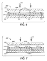
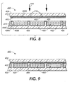
- One example of a suitable manner of securing microcapsules 312 to end portion 310 is by using a suitable adhesive layer (not shown) disposed along end portion 310 , for example, in a manner similar to layer 114 shown in and described with regard to FIGURE 3.
- An arrow 316 indicates displacement of second substrate 304 toward wall microstructure 306 to assemble microcell structure 300 . It will be appreciated that the construction of microcell structure 300, once assembled, will be substantially similar to structure 100 shown in and described with regard to FIGURE 4. However, the plurality of unruptured microcapsules 112A shown in FIGURE 4 will be eliminated or significantly reduced in structure 300 .
- microencapsulation is generally well known by those of skill in the art.
- the microcapsules used in any one application will typically have properties to achieve the objectives of the application.
- the adhesive and microcapsules it is generally desirable for the adhesive and microcapsules to have a relatively high level of optical clarity and/or transparency, with the refractive index being about the same as that of the contents of the microcell to minimize scattering.
Landscapes
- Physics & Mathematics (AREA)
- Nonlinear Science (AREA)
- General Physics & Mathematics (AREA)
- Optics & Photonics (AREA)
- Chemical & Material Sciences (AREA)
- Crystallography & Structural Chemistry (AREA)
- Mathematical Physics (AREA)
- Health & Medical Sciences (AREA)
- Life Sciences & Earth Sciences (AREA)
- Chemical Kinetics & Catalysis (AREA)
- Electrochemistry (AREA)
- Molecular Biology (AREA)
- Electrochromic Elements, Electrophoresis, Or Variable Reflection Or Absorption Elements (AREA)
- Devices For Indicating Variable Information By Combining Individual Elements (AREA)
- Adhesives Or Adhesive Processes (AREA)
Applications Claiming Priority (2)
| Application Number | Priority Date | Filing Date | Title |
|---|---|---|---|
| US10/739,621 US7279064B2 (en) | 2003-12-18 | 2003-12-18 | Method of sealing an array of cell microstructures using microencapsulated adhesive |
| US739621 | 2007-04-24 |
Publications (1)
| Publication Number | Publication Date |
|---|---|
| EP1544668A1 true EP1544668A1 (en) | 2005-06-22 |
Family
ID=34523190
Family Applications (1)
| Application Number | Title | Priority Date | Filing Date |
|---|---|---|---|
| EP20040029259 Withdrawn EP1544668A1 (en) | 2003-12-18 | 2004-12-09 | Method of sealing an array of cell microstructures using microencapsulated adhesive |
Country Status (3)
| Country | Link |
|---|---|
| US (2) | US7279064B2 (https=) |
| EP (1) | EP1544668A1 (https=) |
| JP (1) | JP4562511B2 (https=) |
Cited By (3)
| Publication number | Priority date | Publication date | Assignee | Title |
|---|---|---|---|---|
| CN100430811C (zh) * | 2005-07-29 | 2008-11-05 | 精工爱普生株式会社 | 电泳显示板、电泳显示装置及电泳显示板的制造方法 |
| EP2073057A3 (en) * | 2007-12-17 | 2009-07-15 | Palo Alto Research Center Incorporated | Display |
| EP2074478A4 (en) * | 2007-03-08 | 2011-01-19 | Ricoh Co Ltd | DISPLAY ELEMENT, IMAGE DISPLAY AND PICTURE DISPLAY SYSTEM |
Families Citing this family (34)
| Publication number | Priority date | Publication date | Assignee | Title |
|---|---|---|---|---|
| US7557981B2 (en) * | 2000-03-03 | 2009-07-07 | Sipix Imaging, Inc. | Electrophoretic display and process for its manufacture |
| US6831770B2 (en) * | 2000-03-03 | 2004-12-14 | Sipix Imaging, Inc. | Electrophoretic display and novel process for its manufacture |
| US7715088B2 (en) | 2000-03-03 | 2010-05-11 | Sipix Imaging, Inc. | Electrophoretic display |
| US7052571B2 (en) * | 2000-03-03 | 2006-05-30 | Sipix Imaging, Inc. | Electrophoretic display and process for its manufacture |
| US20070237962A1 (en) * | 2000-03-03 | 2007-10-11 | Rong-Chang Liang | Semi-finished display panels |
| US7158282B2 (en) * | 2000-03-03 | 2007-01-02 | Sipix Imaging, Inc. | Electrophoretic display and novel process for its manufacture |
| US7233429B2 (en) | 2000-03-03 | 2007-06-19 | Sipix Imaging, Inc. | Electrophoretic display |
| US7118838B2 (en) * | 2004-03-26 | 2006-10-10 | Brother International Corporation | Method, apparatus and media for displaying information |
| US7710371B2 (en) * | 2004-12-16 | 2010-05-04 | Xerox Corporation | Variable volume between flexible structure and support surface |
| US7517043B2 (en) * | 2004-12-16 | 2009-04-14 | Xerox Corporation | Fluidic structures |
| KR100700523B1 (ko) * | 2005-02-11 | 2007-03-29 | 엘지전자 주식회사 | 충돌 대전형 전자종이 표시소자 및 그 제조 방법 |
| US7324264B2 (en) * | 2006-02-23 | 2008-01-29 | Eastman Kodak Company | Electro-optical modulating display and method of making the same |
| US20070205979A1 (en) * | 2006-03-02 | 2007-09-06 | Bigelow Donald O | Electro-optical modulating display devices comprising and array of microcells and a method for making such devices |
| US7403325B2 (en) * | 2006-05-19 | 2008-07-22 | Xerox Corporation | Electrophoretic display device |
| JP5263493B2 (ja) * | 2007-09-28 | 2013-08-14 | Nok株式会社 | 燃料電池における部品接合構造 |
| KR101054938B1 (ko) * | 2008-08-11 | 2011-08-05 | 삼성전기주식회사 | 전자종이 표시소자 및 그 제조방법 |
| KR101101518B1 (ko) * | 2009-03-17 | 2012-01-04 | 삼성전기주식회사 | 전기영동 표시장치 및 그 제조방법 |
| KR101043329B1 (ko) * | 2008-08-22 | 2011-06-22 | 삼성전기주식회사 | 전자종이 표시소자 및 그 제조방법 |
| US8159741B2 (en) | 2008-08-22 | 2012-04-17 | Samsung Electro-Mechanics Co., Ltd. | Electronic paper display device and manufacturing method thereof |
| KR101613635B1 (ko) * | 2008-10-31 | 2016-04-20 | 삼성전자주식회사 | 마이크로캡슐, 이를 포함하는 구조체, 이를 포함하는 물품 및 이의 제조 방법 |
| TWI554987B (zh) * | 2010-05-27 | 2016-10-21 | 元太科技工業股份有限公司 | 電子紙顯示器 |
| JP5556497B2 (ja) | 2010-08-17 | 2014-07-23 | 富士ゼロックス株式会社 | 表示媒体、表示媒体の作製方法、及び表示装置 |
| JP2012159634A (ja) * | 2011-01-31 | 2012-08-23 | Mitsubishi Pencil Co Ltd | 電気泳動表示装置の製造方法 |
| US8976349B2 (en) * | 2012-03-30 | 2015-03-10 | Delta Electronics, Inc. | Method of manufacturing particle-based image display |
| JP5904117B2 (ja) * | 2012-12-26 | 2016-04-13 | 富士ゼロックス株式会社 | 表示媒体、表示装置、表示媒体の製造方法 |
| US10087344B2 (en) | 2015-10-30 | 2018-10-02 | E Ink Corporation | Methods for sealing microcell containers with phenethylamine mixtures |
| KR102758806B1 (ko) * | 2016-12-22 | 2025-01-23 | 엘지디스플레이 주식회사 | 게이트 연성 필름을 포함하는 디스플레이 장치 |
| TW201840307A (zh) | 2017-03-24 | 2018-11-16 | 美商伊英克加利福尼亞有限責任公司 | 用於遞送活性分子的微胞系統 |
| WO2019099323A1 (en) * | 2017-11-14 | 2019-05-23 | E Ink California, Llc | Microcell systems for delivering hydrophilic active molecules |
| US11266832B2 (en) | 2017-11-14 | 2022-03-08 | E Ink California, Llc | Electrophoretic active delivery system including porous conductive electrode layer |
| US10973131B2 (en) * | 2018-07-03 | 2021-04-06 | International Business Machines Corporation | Method of manufacturing printed circuit boards |
| KR102797900B1 (ko) | 2019-11-27 | 2025-04-21 | 이 잉크 코포레이션 | 전기 침식 밀봉층을 갖는 마이크로셀들을 포함하는 유익제 전달 시스템 |
| EP4236927A4 (en) | 2020-10-29 | 2024-10-16 | E Ink Corporation | MICROCELL SYSTEMS FOR DELIVERY OF HYDROPHILIC ACTIVE MOLECULES |
| EP4236926A4 (en) | 2020-10-29 | 2024-08-28 | E Ink Corporation | MICROCELL SYSTEMS FOR DELIVERY OF BENEFICIAL AGENTS |
Citations (5)
| Publication number | Priority date | Publication date | Assignee | Title |
|---|---|---|---|---|
| WO2002001281A2 (en) * | 2000-06-28 | 2002-01-03 | Sipix Imaging, Inc. | Manufacturing process for electrophoretic display |
| US20020008898A1 (en) * | 2000-05-30 | 2002-01-24 | Seiko Epson Corporation | Electrophoretic display and method for producing same |
| US20030035885A1 (en) * | 2001-06-04 | 2003-02-20 | Zang Hongmei | Composition and process for the sealing of microcups in roll-to-roll display manufacturing |
| WO2003069407A1 (en) * | 2002-02-18 | 2003-08-21 | Synelec Telecom Multimedia | Display screen and its method of production |
| JP2004326011A (ja) | 2003-04-28 | 2004-11-18 | Bridgestone Corp | 画像表示装置の製造方法及び画像表示装置 |
Family Cites Families (10)
| Publication number | Priority date | Publication date | Assignee | Title |
|---|---|---|---|---|
| JPS63273680A (ja) * | 1987-04-30 | 1988-11-10 | Kyocera Corp | カプセル型接着剤およびカプセル型接着剤を用いた接着方法 |
| JP2906612B2 (ja) * | 1990-08-10 | 1999-06-21 | 富士通株式会社 | マイクロカプセル型導電性接着剤と接着方法 |
| JPH0675211A (ja) * | 1992-08-26 | 1994-03-18 | Sharp Corp | 光学部品の接着方法 |
| US6930818B1 (en) | 2000-03-03 | 2005-08-16 | Sipix Imaging, Inc. | Electrophoretic display and novel process for its manufacture |
| JP2002174831A (ja) * | 2000-12-07 | 2002-06-21 | Minolta Co Ltd | 可逆性画像表示媒体及びその製作方法 |
| DK1229181T3 (da) * | 2001-02-02 | 2006-02-20 | Fritz Egger Gmbh & Co | Bygningskomponent og fremgangsmåde til fremstilling af en sådan bygningskomponent |
| US6577433B1 (en) * | 2002-01-16 | 2003-06-10 | Xerox Corporation | Electrophoretic displays, display fluids for use therein, and methods of displaying images |
| US7123238B2 (en) * | 2002-01-16 | 2006-10-17 | Xerox Corporation | Spacer layer for electrophoretic display device |
| FR2836242B1 (fr) * | 2002-02-18 | 2004-04-30 | Synelec Telecom Multimedia | Procede de fabrication d'un ecran de retroprojection |
| TWI270835B (en) * | 2002-10-29 | 2007-01-11 | Matsushita Electric Industrial Co Ltd | Display device and generation method of image display particle |
-
2003
- 2003-12-18 US US10/739,621 patent/US7279064B2/en not_active Expired - Fee Related
-
2004
- 2004-12-09 EP EP20040029259 patent/EP1544668A1/en not_active Withdrawn
- 2004-12-17 JP JP2004366900A patent/JP4562511B2/ja not_active Expired - Fee Related
-
2007
- 2007-08-31 US US11/848,591 patent/US7583430B2/en not_active Expired - Fee Related
Patent Citations (5)
| Publication number | Priority date | Publication date | Assignee | Title |
|---|---|---|---|---|
| US20020008898A1 (en) * | 2000-05-30 | 2002-01-24 | Seiko Epson Corporation | Electrophoretic display and method for producing same |
| WO2002001281A2 (en) * | 2000-06-28 | 2002-01-03 | Sipix Imaging, Inc. | Manufacturing process for electrophoretic display |
| US20030035885A1 (en) * | 2001-06-04 | 2003-02-20 | Zang Hongmei | Composition and process for the sealing of microcups in roll-to-roll display manufacturing |
| WO2003069407A1 (en) * | 2002-02-18 | 2003-08-21 | Synelec Telecom Multimedia | Display screen and its method of production |
| JP2004326011A (ja) | 2003-04-28 | 2004-11-18 | Bridgestone Corp | 画像表示装置の製造方法及び画像表示装置 |
Cited By (4)
| Publication number | Priority date | Publication date | Assignee | Title |
|---|---|---|---|---|
| CN100430811C (zh) * | 2005-07-29 | 2008-11-05 | 精工爱普生株式会社 | 电泳显示板、电泳显示装置及电泳显示板的制造方法 |
| EP2074478A4 (en) * | 2007-03-08 | 2011-01-19 | Ricoh Co Ltd | DISPLAY ELEMENT, IMAGE DISPLAY AND PICTURE DISPLAY SYSTEM |
| US7936498B2 (en) | 2007-03-08 | 2011-05-03 | Ricoh Company, Ltd. | Display element, image display device, and image display system |
| EP2073057A3 (en) * | 2007-12-17 | 2009-07-15 | Palo Alto Research Center Incorporated | Display |
Also Published As
| Publication number | Publication date |
|---|---|
| JP4562511B2 (ja) | 2010-10-13 |
| US7279064B2 (en) | 2007-10-09 |
| JP2005182043A (ja) | 2005-07-07 |
| US20070286986A1 (en) | 2007-12-13 |
| US7583430B2 (en) | 2009-09-01 |
| US20050133154A1 (en) | 2005-06-23 |
Similar Documents
| Publication | Publication Date | Title |
|---|---|---|
| US7583430B2 (en) | Method of sealing an array of cell microstructures using microencapsulated adhesive | |
| US10072185B2 (en) | Self-heating sealant or adhesive employing multi-compartment microcapsules | |
| US9835925B1 (en) | Electro-optic displays, and processes for the production thereof | |
| JP4519124B2 (ja) | 微小流動性デバイスの内部の壁 | |
| CN1203353C (zh) | 制造电泳显示器的方法 | |
| Singha et al. | Surfactant-mediated collapse of liquid marbles and directed assembly of particles at the liquid surface | |
| CN102402093B (zh) | 电光显示装置及其制造方法 | |
| JP5157200B2 (ja) | ハニカム構造シートの製造方法及び表示パネルの製造方法 | |
| US9896389B2 (en) | Heat-generating multi-compartment microcapsules | |
| CN102289125A (zh) | 电泳显示装置 | |
| Zhang et al. | Liquid marbles under electric fields: New capabilities for non-wetting droplet manipulation and beyond | |
| Lekshmi et al. | Droplet-impact driven formation of ultralow volume liquid marbles with enhanced mechanical stability and sensing ability | |
| US20050045539A1 (en) | Control device and method for controlling liquid droplets | |
| JP4608816B2 (ja) | 表示装置の製造方法 | |
| CN114265256A (zh) | 一种电子纸显示设备的制造方法及电子纸显示设备 | |
| Song et al. | Control of orientation, formation of ordered structures, and self-sorting of surface-functionalized microcubes at the air–water interface | |
| Sakurai et al. | Aqueous Bubbles Stabilized with Millimeter-Sized Polymer Plates | |
| WO2008039140A1 (en) | A cell for confinement of very small volumes of soft matter and fluids | |
| JP5533384B2 (ja) | 電気泳動粒子を含む分散液を封入する封入方法 | |
| JP2004524570A (ja) | 電気泳動媒体 | |
| CN118131544A (zh) | 电子纸显示面板和制备方法 | |
| CN116018553B (zh) | 用于电泳显示器的反射性微单元及其制造方法 | |
| TWI815316B (zh) | 製造用於電泳顯示器之積層體之方法 | |
| EP1537910A1 (en) | Method and apparatus for forming a chemical gradient on a substrate | |
| US20060022367A1 (en) | Display element and manufacturing method thereof |
Legal Events
| Date | Code | Title | Description |
|---|---|---|---|
| PUAI | Public reference made under article 153(3) epc to a published international application that has entered the european phase |
Free format text: ORIGINAL CODE: 0009012 |
|
| AK | Designated contracting states |
Kind code of ref document: A1 Designated state(s): AT BE BG CH CY CZ DE DK EE ES FI FR GB GR HU IE IS IT LI LT LU MC NL PL PT RO SE SI SK TR |
|
| AX | Request for extension of the european patent |
Extension state: AL BA HR LV MK YU |
|
| 17P | Request for examination filed |
Effective date: 20051222 |
|
| AKX | Designation fees paid |
Designated state(s): DE FR GB |
|
| 17Q | First examination report despatched |
Effective date: 20110120 |
|
| STAA | Information on the status of an ep patent application or granted ep patent |
Free format text: STATUS: THE APPLICATION IS DEEMED TO BE WITHDRAWN |
|
| 18D | Application deemed to be withdrawn |
Effective date: 20150804 |