EP1540362B1 - Magnetic sensing device - Google Patents
Magnetic sensing device Download PDFInfo
- Publication number
- EP1540362B1 EP1540362B1 EP03784822A EP03784822A EP1540362B1 EP 1540362 B1 EP1540362 B1 EP 1540362B1 EP 03784822 A EP03784822 A EP 03784822A EP 03784822 A EP03784822 A EP 03784822A EP 1540362 B1 EP1540362 B1 EP 1540362B1
- Authority
- EP
- European Patent Office
- Prior art keywords
- magnetic
- integrated circuit
- layer
- magnetic sensing
- sensing device
- Prior art date
- Legal status (The legal status is an assumption and is not a legal conclusion. Google has not performed a legal analysis and makes no representation as to the accuracy of the status listed.)
- Expired - Lifetime
Links
- 230000005291 magnetic effect Effects 0.000 title claims description 179
- 239000000463 material Substances 0.000 claims description 22
- 229910052751 metal Inorganic materials 0.000 claims description 15
- 239000002184 metal Substances 0.000 claims description 15
- 230000013011 mating Effects 0.000 claims description 11
- 229910000595 mu-metal Inorganic materials 0.000 claims description 5
- 229910000889 permalloy Inorganic materials 0.000 claims description 5
- 239000007769 metal material Substances 0.000 claims description 3
- 230000005672 electromagnetic field Effects 0.000 description 11
- PXHVJJICTQNCMI-UHFFFAOYSA-N Nickel Chemical compound [Ni] PXHVJJICTQNCMI-UHFFFAOYSA-N 0.000 description 9
- XEEYBQQBJWHFJM-UHFFFAOYSA-N Iron Chemical compound [Fe] XEEYBQQBJWHFJM-UHFFFAOYSA-N 0.000 description 7
- 238000000034 method Methods 0.000 description 6
- 229910052759 nickel Inorganic materials 0.000 description 5
- 230000008569 process Effects 0.000 description 5
- 230000008859 change Effects 0.000 description 4
- 239000010949 copper Substances 0.000 description 4
- 229910052742 iron Inorganic materials 0.000 description 4
- 238000005259 measurement Methods 0.000 description 4
- 238000010521 absorption reaction Methods 0.000 description 3
- 239000002800 charge carrier Substances 0.000 description 3
- 229910052802 copper Inorganic materials 0.000 description 3
- 238000000623 plasma-assisted chemical vapour deposition Methods 0.000 description 3
- RYGMFSIKBFXOCR-UHFFFAOYSA-N Copper Chemical compound [Cu] RYGMFSIKBFXOCR-UHFFFAOYSA-N 0.000 description 2
- BOTDANWDWHJENH-UHFFFAOYSA-N Tetraethyl orthosilicate Chemical compound CCO[Si](OCC)(OCC)OCC BOTDANWDWHJENH-UHFFFAOYSA-N 0.000 description 2
- 238000001505 atmospheric-pressure chemical vapour deposition Methods 0.000 description 2
- 230000015572 biosynthetic process Effects 0.000 description 2
- 238000005229 chemical vapour deposition Methods 0.000 description 2
- 239000011651 chromium Substances 0.000 description 2
- 239000004020 conductor Substances 0.000 description 2
- 238000000151 deposition Methods 0.000 description 2
- 238000010586 diagram Methods 0.000 description 2
- 239000003302 ferromagnetic material Substances 0.000 description 2
- 238000007737 ion beam deposition Methods 0.000 description 2
- 238000004518 low pressure chemical vapour deposition Methods 0.000 description 2
- 239000011572 manganese Substances 0.000 description 2
- 230000035699 permeability Effects 0.000 description 2
- 230000035945 sensitivity Effects 0.000 description 2
- VYZAMTAEIAYCRO-UHFFFAOYSA-N Chromium Chemical compound [Cr] VYZAMTAEIAYCRO-UHFFFAOYSA-N 0.000 description 1
- 229910017881 Cu—Ni—Fe Inorganic materials 0.000 description 1
- 238000006842 Henry reaction Methods 0.000 description 1
- PWHULOQIROXLJO-UHFFFAOYSA-N Manganese Chemical compound [Mn] PWHULOQIROXLJO-UHFFFAOYSA-N 0.000 description 1
- 229910003271 Ni-Fe Inorganic materials 0.000 description 1
- XUIMIQQOPSSXEZ-UHFFFAOYSA-N Silicon Chemical compound [Si] XUIMIQQOPSSXEZ-UHFFFAOYSA-N 0.000 description 1
- QVGXLLKOCUKJST-UHFFFAOYSA-N atomic oxygen Chemical compound [O] QVGXLLKOCUKJST-UHFFFAOYSA-N 0.000 description 1
- 229910052804 chromium Inorganic materials 0.000 description 1
- 229910017052 cobalt Inorganic materials 0.000 description 1
- 239000010941 cobalt Substances 0.000 description 1
- GUTLYIVDDKVIGB-UHFFFAOYSA-N cobalt atom Chemical compound [Co] GUTLYIVDDKVIGB-UHFFFAOYSA-N 0.000 description 1
- 230000000295 complement effect Effects 0.000 description 1
- 238000010276 construction Methods 0.000 description 1
- 230000005684 electric field Effects 0.000 description 1
- 238000004070 electrodeposition Methods 0.000 description 1
- 238000005516 engineering process Methods 0.000 description 1
- 230000004907 flux Effects 0.000 description 1
- 229910052746 lanthanum Inorganic materials 0.000 description 1
- FZLIPJUXYLNCLC-UHFFFAOYSA-N lanthanum atom Chemical compound [La] FZLIPJUXYLNCLC-UHFFFAOYSA-N 0.000 description 1
- 230000005426 magnetic field effect Effects 0.000 description 1
- 229910052748 manganese Inorganic materials 0.000 description 1
- 238000004519 manufacturing process Methods 0.000 description 1
- 229910044991 metal oxide Inorganic materials 0.000 description 1
- 150000004706 metal oxides Chemical class 0.000 description 1
- 150000002739 metals Chemical class 0.000 description 1
- 229910052760 oxygen Inorganic materials 0.000 description 1
- 239000001301 oxygen Substances 0.000 description 1
- 238000005498 polishing Methods 0.000 description 1
- 239000004065 semiconductor Substances 0.000 description 1
- 229910052710 silicon Inorganic materials 0.000 description 1
- 239000010703 silicon Substances 0.000 description 1
- 239000002210 silicon-based material Substances 0.000 description 1
- 229910052712 strontium Inorganic materials 0.000 description 1
- CIOAGBVUUVVLOB-UHFFFAOYSA-N strontium atom Chemical compound [Sr] CIOAGBVUUVVLOB-UHFFFAOYSA-N 0.000 description 1
- 239000000126 substance Substances 0.000 description 1
- 238000007740 vapor deposition Methods 0.000 description 1
Images


Classifications
-
- G—PHYSICS
- G01—MEASURING; TESTING
- G01R—MEASURING ELECTRIC VARIABLES; MEASURING MAGNETIC VARIABLES
- G01R33/00—Arrangements or instruments for measuring magnetic variables
- G01R33/02—Measuring direction or magnitude of magnetic fields or magnetic flux
- G01R33/06—Measuring direction or magnitude of magnetic fields or magnetic flux using galvano-magnetic devices
- G01R33/09—Magnetoresistive devices
-
- Y—GENERAL TAGGING OF NEW TECHNOLOGICAL DEVELOPMENTS; GENERAL TAGGING OF CROSS-SECTIONAL TECHNOLOGIES SPANNING OVER SEVERAL SECTIONS OF THE IPC; TECHNICAL SUBJECTS COVERED BY FORMER USPC CROSS-REFERENCE ART COLLECTIONS [XRACs] AND DIGESTS
- Y10—TECHNICAL SUBJECTS COVERED BY FORMER USPC
- Y10T—TECHNICAL SUBJECTS COVERED BY FORMER US CLASSIFICATION
- Y10T428/00—Stock material or miscellaneous articles
- Y10T428/11—Magnetic recording head
- Y10T428/1193—Magnetic recording head with interlaminar component [e.g., adhesion layer, etc.]
Definitions
- the present invention relates to magnetic sensors, and more particularly, to shielding a magnetic sensing device from electromagnetic signals generated from within.
- Magnetic sensors are typically used for direction finding or other means of navigation.
- the technology for sensing magnetic fields has evolved due to the need for improved sensitivity, smaller size, and compatibility with electronic systems.
- MR magnetoresistive
- MR sensors provide a solid-state solution for building compass navigation systems. Their high sensitivity and effective repeatability, along with small size, results in a high accuracy magnetic sensor. However, integrating an MR sensor with electronic circuitry may not result in accurate magnetic measurements. Electromagnetic signals, such as current signals, within the electronic circuitry may interfere with signals from the Earth's magnetic field, and therefore, an accurate measurement of the Earth's magnetic field may not be obtained. An electric current always produces a magnetic field, which will interfere with a measurement of a low intensity magnetic field.
- Existing MR sensor systems lack an ability to eliminate or reduce the magnetic field effects generated by electronics within the system, and so it is desirable to provide a device that eliminates stray electromagnetic signals in order to accurately measure a magnetic field.
- US-A-5041780 , US-A-5570015 and EP-A-0390582 all disclose magnetic sensing devices with sensing layers.
- a magnetic sensing device comprising:
- a magnetic sensing device may accurately measure magnetic fields while in close proximity, to an integrated circuit.
- the magnetic sensing device may have a magnetic sensor mounted over an integrated circuit to produce a system-on-a-chip.
- a magnetic shielding layer and/or magnetic absorption layer may be deposited between the magnetic sensor and the integrated circuit to provide a buffer layer that reduces and/or eliminates stray electromagnetic signals generated by the integrated circuit.
- the magnetic sensor may accurately measure a magnetic field external to the device, which is independent of a magnetic field generated by electrical currents within the integrated circuit.
- FIG. 1 an exemplary embodiment of a magnetic sensing system 100 is illustrated. While FIG. 1 illustrates the magnetic sensing system 100, other packages and/or a combination of sensors may be used as well. In addition, it should be understood that the magnetic sensing system 100 illustrated in FIG. 1 and other arrangements described herein are set forth for purposes of example only, and other arrangements and elements can be used instead and some elements may be omitted altogether, depending on manufacturing and/or consumer preferences.
- the magnetic sensing system 100 has an integrated circuit 102, a magnetic buffer layer 104, and a magnetic sensor 106.
- the integrated circuit 102, the magnetic buffer layer 104, and the magnetic sensor 106 may all be enclosed within a package 108, such as a plastic package, an electronic integrated circuit package that has multiple pin-outs, or a nonmagnetic molded package.
- the package may also be a small outline integrated circuit (SOIC) package that has a copper lead frame.
- SOIC small outline integrated circuit
- the magnetic sensing system 100 may also contain other sensing and/or electronic elements.
- the magnetic buffer layer 104 is positioned over the integrated circuit 102 and the magnetic sensor 106 is positioned over the magnetic buffer layer 104.
- the magnetic sensor 106 may be positioned to be substantially aligned with the integrated circuit 102, or the magnetic sensor 106 may be positioned to be directly over the integrated circuit 102.
- the magnetic sensor 106, magnetic buffer layer 104, and the integrated circuit 102 may be positioned in entirely different arrangements as well. However, in the exemplary embodiment, it may be necessary to at least position the magnetic buffer layer 104 between the magnetic sensor 106 and the integrated circuit 102.
- the integrated circuit 102 of the magnetic sensing system 100 may be a printed circuit board (PCB), an electronics board, an integrated circuit chip, or any integrated circuit operable to process electrical signals.
- the integrated circuit 102 may be a piece of silicon material or a complementary metal-oxide semiconductor (CMOS) bipolar material.
- CMOS complementary metal-oxide semiconductor
- the integrated circuit 102 may have both analog and digital outputs and may include components such as op-amps, amplifiers, or other signal-conditioning electronics.
- the integrated circuit 102 may also be other types of circuitry as well.
- a magnetic field is generated by the integrated circuit 102 when electric charge carriers, i.e. electrons, move through electrical conductors (e.g., traces) of the integrated circuit 102.
- an electric current can produce a magnetic field.
- a pulsating direct current, or an alternating current characteristically produces an electromagnetic field.
- charge carriers are accelerated (as opposed to moving at a constant velocity)
- a fluctuating magnetic field may be produced.
- This generates a fluctuating electric field, which in turn produces another varying magnetic field. This results in a growing electromagnetic field which may continue to grow without bound as the charge carriers continue to accelerate.
- the magnetic buffer layer 104 may either shield the magnetic sensor 106 from electromagnetic fields generated by current flow within the integrated circuit 102, and/or the magnetic buffer layer 104 may absorb the electromagnetic fields generated by the integrated circuit 102.
- the magnetic buffer layer 104 may also shield and/or absorb electromagnetic fields generated by other internal sources of the magnetic sensing system 100.
- the magnetic buffer layer 104 may comprise a permalloy material.
- the magnetic buffer layer 104 may comprise a Mu-metal material.
- the magnetic buffer layer 104 may comprise any material with a high magnetic permeability (i.e., a high ratio of the magnetic flux density to the magnetic field strength) and/or any magnetic resistant material.
- a permalloy material is typically comprised of nickel and iron.
- the magnetic buffer layer 104 is comprised of a permalloy material composition that has about 60-80% nickel (Ni), 10-20% iron (Fe), 5-10% copper (Cu), and 5-10% cobalt (Co) (wt. %).
- the permalloy material composition may also be between 50-80% nickel and the balance iron.
- a Mu-metal is a soft ferromagnetic material.
- the magnetic buffer layer 104 may be a Mu-metal material with approximately 77% Ni, 16 % Fe, 5% Cu, and 2% chromium (Cr).
- Other Mu-metals may be used as well, such as Ni-Fe based metals with amounts of silicon (Si) and/or other similar elements added. Other elements may also be used.
- the magnetic buffer layer 104 may be any ferromagnetic material that has a high magnetic permeability such as, for example, on the order of 10 4 H/m (Henries per meter). Other examples are possible as well.
- the magnetic buffer layer 104 may be approximately a few hundred angstroms in thickness, although the thickness may be more or less than a few hundred angstroms. For example, for a magnetic sensing system designed to measure the Earth's magnetic field, the magnetic buffer layer 104 may be approximately 100-500 angstroms.
- the magnetic buffer layer 104 may be deposited onto a mating surface of the integrated circuit 102 by an electro-deposition process such as pressure vapor deposition (PVD) or ion-beam deposition.
- the magnetic buffer layer 104 may be deposited onto the integrated circuit 102 by a chemical vapor deposition (CVD), an atmospheric pressure chemical vapor deposition (APCVD), a low-pressure chemical vapor deposition (LPCVD), a plasma enhanced chemical vapor deposition (PECVD), or other deposition techniques.
- the magnetic buffer layer 104 may be deposited only in an area between the integrated circuit 102 and the magnetic sensor 106 or possibly onto a greater area of the integrated circuit 102 to reduce and/or eliminate stray or leakage current and/or magnetic fields.
- the magnetic buffer layer 104 may be deposited over the entire mating surface of the integrated circuit 102, as defined by the area between the integrated circuit 102 and the magnetic sensor 106 or as defined by the entire surface area of the integrated circuit 102.
- the magnetic buffer layer 104 may enable the magnetic sensor 106 to measure an accurate magnetic field strength or a magnetic field direction.
- the magnetic sensor 106 may measure a highly sensitive magnetic field, such as the Earth's magnetic field, which is typically about 0.5 to 0.6 Gauss or approximately 5 x 10 -5 Tesla.
- the magnetic sensor 106 may be a thin layer of an anisotropic magnetoresistive (AMR) film material, such as 81 % Ni and 19% Fe.
- AMR anisotropic magnetoresistive
- the AMR film may have a 2-3% change in resistance when exposed to a magnetic field.
- the magnetic sensor 106 may also be a giant magnetoresistive (GMR) film material, which may comprise a Ni-Fe-Cu-Ni-Fe stack or any other combination, and may have a 3-100% change in resistance when exposed to a magnetic field.
- the magnetic sensor 106 may be a colossal magnetoresistive (CMR) film material, which may comprise lanthanum (La), strontium (Sr), manganese (Mn), and oxygen (O).
- the magnetic sensor 106 may comprise other materials as well.
- the magnetic sensor 106 may have a thickness less than approximately 200 angstroms.
- a layer of the film materials comprising the magnetic sensor 106 may be deposited over the magnetic buffer layer 104 and a desired formation of the magnetic sensor 106 may be etched within the layer of the film materials.
- the magnetic sensor 106 may be deposited on the magnetic buffer layer 104 using a PVD or ion-beam deposition process.
- the magnetic sensor 106 may include a resistive Wheatstone bridge formed by a magnetoresistive metal film. When a power supply is connected to the bridge, the magnetic sensor 106 may convert any ambient or applied magnetic field in the sensitive direction to a voltage output.
- the magnetic buffer layer 104 may enable the magnetic sensor 106 to be mounted directly over or in close proximity to the integrated circuit 102 and still maintain the ability to detect a sensitive magnetic field.
- the magnetic buffer layer 104 may prevent electromagnetic fields generated by the integrated circuit 102 from disturbing electromagnetic fields external from the magnetic sensing system 100. Without an electromagnetic shielding or absorbing layer between the magnetic sensor 106 and the integrated circuit 102, the electromagnetic fields generated by current flow within the integrated circuit 102 could saturate the magnetic sensor 106 and disallow the magnetic sensor 106 to detect an electromagnetic field external to the magnetic sensing system 100.
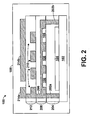
- FIG. 2 a detailed illustration of the magnetic sensing system 100 illustrated in FIG. 1 is shown.
- the integrated circuit 102 is mounted to a base of the package 108 and the magnetic buffer layer 104 is deposited onto the integrated circuit 102.
- First metal interconnects 202(a-b) are deposited over the magnetic buffer layer 104 and the integrated circuit 102.
- a dielectric layer 204 is deposited over the magnetic buffer layer 104 and the integrated circuit 102 and around the first metal interconnects 202(a-b).
- the magnetic sensor 106 may be deposited onto the dielectric layer 204 and etched to a desired formation. For example, as illustrated in FIG. 2 , the magnetic sensor 106 comprises three small parallel sections.
- a second metal interconnect 206 is deposited over the magnetic sensor 106 in a manner such that it contacts the first metal interconnects 202(a-b).
- Another dielectric layer 208 is deposited over the dielectric layer 204 and the second metal interconnect 206.
- a third metal interconnect 210 is deposited over the dielectric layer 208 in a manner such that it contacts the second metal interconnect 206.
- Another dielectric layer 212 is deposited over the third metal interconnect 210 and output metal interconnects 214(a-b) are deposited over the dielectric layer 212 such that the output metal interconnects 214(a-b) contact the third metal interconnect 210.
- the number of dielectric layers and metal interconnects described within the magnetic sensing system 100 are not critical to all embodiments of the invention, however, as other arrangements may still achieve advantages of the invention.
- the construction described herein, namely a packaged integrated circuit arrangement is just one example of the many different forms that may be used.
- the dielectric layers 204, 208, and 212 may comprise a tetra-ethyl-ortho-silicate (TEOS) material or other insulating and/or non-conducting materials.
- TEOS tetra-ethyl-ortho-silicate
- the dielectric layers 204, 208, and 212 can be approximately 1-2 microns thick.
- CMP chemical mechanical polishing
- a chemical mechanical polishing (CMP) process may be completed to smooth, flatten, and/or eliminate imperfections on the surfaces to which the dielectric layers 204, 208, and 212 may be deposited.
- the dielectric layers 204, 208, and 212 may be deposited using a PECVD process.
- a method 300 of internally shielding a magnetic sensing device is illustrated.
- a surface of an integrated circuit to which a layer of magnetic resistant material may be deposited is cleaned.
- the layer of magnetic resistant material may then be deposited upon the integrated circuit as shown at block 304, and a dielectric layer of material may be deposited onto the magnetic resistant layer, as shown at block 306.
- a magnetic sensing layer of material is then deposited onto the dielectric layer as shown at block 308, and the integrated circuit and magnetic sensor may then be packaged as shown at block 310.
- the layer of magnetic resistant material is deposited between the magnetic sensing layer and the integrated circuit to absorb electromagnetic signals generated by the integrated circuit.
- Incorporating a magnetic resistant material between the magnetic sensor and the integrated circuit may eliminate the need to compensate for a magnetic field measurement distortion due to magnetic fields generated by internal sources of a sensing system.
Landscapes
- Physics & Mathematics (AREA)
- Condensed Matter Physics & Semiconductors (AREA)
- General Physics & Mathematics (AREA)
- Measuring Magnetic Variables (AREA)
- Hall/Mr Elements (AREA)
Applications Claiming Priority (3)
| Application Number | Priority Date | Filing Date | Title |
|---|---|---|---|
| US201381 | 2002-07-23 | ||
| US10/201,381 US7037604B2 (en) | 2002-07-23 | 2002-07-23 | Magnetic sensing device |
| PCT/US2003/023389 WO2004015437A1 (en) | 2002-07-23 | 2003-07-23 | Magnetic sensing device |
Publications (2)
| Publication Number | Publication Date |
|---|---|
| EP1540362A1 EP1540362A1 (en) | 2005-06-15 |
| EP1540362B1 true EP1540362B1 (en) | 2009-05-27 |
Family
ID=30769637
Family Applications (1)
| Application Number | Title | Priority Date | Filing Date |
|---|---|---|---|
| EP03784822A Expired - Lifetime EP1540362B1 (en) | 2002-07-23 | 2003-07-23 | Magnetic sensing device |
Country Status (8)
| Country | Link |
|---|---|
| US (1) | US7037604B2 (enExample) |
| EP (1) | EP1540362B1 (enExample) |
| JP (1) | JP2005534193A (enExample) |
| CN (1) | CN1672058A (enExample) |
| AU (1) | AU2003265301A1 (enExample) |
| CA (1) | CA2493438A1 (enExample) |
| DE (1) | DE60327781D1 (enExample) |
| WO (1) | WO2004015437A1 (enExample) |
Families Citing this family (26)
| Publication number | Priority date | Publication date | Assignee | Title |
|---|---|---|---|---|
| US20040037818A1 (en) * | 1998-07-30 | 2004-02-26 | Brand Stephen J. | Treatment for diabetes |
| US7239000B2 (en) * | 2003-04-15 | 2007-07-03 | Honeywell International Inc. | Semiconductor device and magneto-resistive sensor integration |
| US6883241B2 (en) * | 2003-07-31 | 2005-04-26 | Medtronic, Inc. | Compass-based indicator with magnetic shielding |
| US7126330B2 (en) * | 2004-06-03 | 2006-10-24 | Honeywell International, Inc. | Integrated three-dimensional magnetic sensing device and method to fabricate an integrated three-dimensional magnetic sensing device |
| KR20060021649A (ko) * | 2004-09-03 | 2006-03-08 | 엘지전자 주식회사 | 고밀도 미세 패턴의 단락 도선 위치 검출을 위한 자기 센서 |
| US7064558B1 (en) * | 2004-12-16 | 2006-06-20 | Honeywell International Inc. | Millivolt output circuit for use with programmable sensor compensation integrated circuits |
| DE102005047414B4 (de) | 2005-02-21 | 2012-01-05 | Infineon Technologies Ag | Magnetoresistives Sensormodul und Verfahren zum Herstellen desselben |
| US7545662B2 (en) * | 2005-03-25 | 2009-06-09 | Taiwan Semiconductor Manufacturing Co., Ltd. | Method and system for magnetic shielding in semiconductor integrated circuit |
| DE602005017900D1 (de) * | 2005-10-10 | 2010-01-07 | Infineon Technologies Sensonor | Niederfrequenzempfänger mit Magnetfelddetektor |
| TWI295102B (en) * | 2006-01-13 | 2008-03-21 | Ind Tech Res Inst | Multi-functional substrate structure |
| SG135077A1 (en) * | 2006-02-27 | 2007-09-28 | Nanyang Polytechnic | Apparatus and method for non-invasively sensing pulse rate and blood flow anomalies |
| BRPI0605714B1 (pt) * | 2006-03-07 | 2018-06-26 | José Gouveia Abrunhosa Jorge | Dispositivo e processo para detecção de materiais magnéticos em sistemas antifurtos de tecnologia eletromagnética |
| EP2360489B1 (en) * | 2010-02-04 | 2013-04-17 | Nxp B.V. | Magnetic field sensor |
| TWI467821B (zh) * | 2010-12-31 | 2015-01-01 | Voltafield Technology Corp | 磁阻感測器及其製造方法 |
| TWI443360B (zh) * | 2011-02-22 | 2014-07-01 | Voltafield Technology Corp | 磁阻感測器及其製造方法 |
| US20140347047A1 (en) * | 2011-02-22 | 2014-11-27 | Voltafield Technology Corporation | Magnetoresistive sensor |
| ITTO20120614A1 (it) * | 2012-07-11 | 2014-01-12 | St Microelectronics Srl | Sensore magnetoresistivo integrato multistrato e relativo metodo di fabbricazione |
| EP2878966B1 (en) * | 2013-03-26 | 2017-07-26 | Asahi Kasei Microdevices Corporation | Magnetic sensor and magnetic detecting method |
| DE202013003631U1 (de) * | 2013-04-18 | 2013-04-26 | Steiner-Optik Gmbh | Batteriefachschirmung |
| US10180341B2 (en) * | 2013-10-24 | 2019-01-15 | The United States Of America As Represented By The Administrator Of Nasa | Multi-layer wireless sensor construct for use at electrically-conductive material surfaces |
| US10193228B2 (en) | 2013-10-24 | 2019-01-29 | The United States Of America As Represented By The Administrator Of Nasa | Antenna for near field sensing and far field transceiving |
| US9497846B2 (en) * | 2013-10-24 | 2016-11-15 | The United States Of America As Represented By The Administrator Of The National Aeronautics And Space Administration | Plasma generator using spiral conductors |
| CN103647022B (zh) * | 2013-12-25 | 2016-04-27 | 杭州士兰集成电路有限公司 | 各向异性磁阻传感器垂直结构及其制造方法 |
| US10145906B2 (en) | 2015-12-17 | 2018-12-04 | Analog Devices Global | Devices, systems and methods including magnetic structures |
| CN106229406A (zh) * | 2016-10-10 | 2016-12-14 | 杭州士兰集成电路有限公司 | 集成型磁开关及其制造方法 |
| US10591320B2 (en) * | 2017-12-11 | 2020-03-17 | Nxp B.V. | Magnetoresistive sensor with stray field cancellation and systems incorporating same |
Family Cites Families (20)
| Publication number | Priority date | Publication date | Assignee | Title |
|---|---|---|---|---|
| US5041780A (en) * | 1988-09-13 | 1991-08-20 | California Institute Of Technology | Integrable current sensors |
| JPH02129882U (enExample) | 1989-03-31 | 1990-10-25 | ||
| US5247278A (en) * | 1991-11-26 | 1993-09-21 | Honeywell Inc. | Magnetic field sensing device |
| US5570015A (en) * | 1992-02-05 | 1996-10-29 | Mitsubishi Denki Kabushiki Kaisha | Linear positional displacement detector for detecting linear displacement of a permanent magnet as a change in direction of magnetic sensor unit |
| US5757591A (en) * | 1996-11-25 | 1998-05-26 | International Business Machines Corporation | Magnetoresistive read/inductive write magnetic head assembly fabricated with silicon on hard insulator for improved durability and electrostatic discharge protection and method for manufacturing same |
| US5902690A (en) * | 1997-02-25 | 1999-05-11 | Motorola, Inc. | Stray magnetic shielding for a non-volatile MRAM |
| US5898548A (en) * | 1997-10-24 | 1999-04-27 | International Business Machines Corporation | Shielded magnetic tunnel junction magnetoresistive read head |
| JPH11154309A (ja) * | 1997-11-20 | 1999-06-08 | Sony Corp | 磁気抵抗効果型磁気ヘッド |
| US6048739A (en) * | 1997-12-18 | 2000-04-11 | Honeywell Inc. | Method of manufacturing a high density magnetic memory device |
| US6072382A (en) * | 1998-01-06 | 2000-06-06 | Nonvolatile Electronics, Incorporated | Spin dependent tunneling sensor |
| CN1451157A (zh) | 1999-10-05 | 2003-10-22 | 西加特技术有限责任公司 | 用于保护磁阻磁头避免静电放电的集成板上器件和方法 |
| US6462541B1 (en) | 1999-11-12 | 2002-10-08 | Nve Corporation | Uniform sense condition magnetic field sensor using differential magnetoresistance |
| WO2001071713A1 (en) * | 2000-03-22 | 2001-09-27 | Nve Corporation | Read heads in planar monolithic integrated circuit chips |
| US6452253B1 (en) * | 2000-08-31 | 2002-09-17 | Micron Technology, Inc. | Method and apparatus for magnetic shielding of an integrated circuit |
| US6717241B1 (en) * | 2000-08-31 | 2004-04-06 | Micron Technology, Inc. | Magnetic shielding for integrated circuits |
| US6515352B1 (en) * | 2000-09-25 | 2003-02-04 | Micron Technology, Inc. | Shielding arrangement to protect a circuit from stray magnetic fields |
| JP3659898B2 (ja) * | 2000-11-27 | 2005-06-15 | Tdk株式会社 | 薄膜磁気ヘッドおよびその製造方法 |
| JP2002184945A (ja) * | 2000-12-11 | 2002-06-28 | Fuji Electric Co Ltd | 磁気素子一体型半導体デバイス |
| US6724027B2 (en) * | 2002-04-18 | 2004-04-20 | Hewlett-Packard Development Company, L.P. | Magnetic shielding for MRAM devices |
| US6936763B2 (en) * | 2002-06-28 | 2005-08-30 | Freescale Semiconductor, Inc. | Magnetic shielding for electronic circuits which include magnetic materials |
-
2002
- 2002-07-23 US US10/201,381 patent/US7037604B2/en not_active Expired - Fee Related
-
2003
- 2003-07-23 CA CA002493438A patent/CA2493438A1/en not_active Abandoned
- 2003-07-23 WO PCT/US2003/023389 patent/WO2004015437A1/en not_active Ceased
- 2003-07-23 JP JP2004527657A patent/JP2005534193A/ja not_active Withdrawn
- 2003-07-23 DE DE60327781T patent/DE60327781D1/de not_active Expired - Fee Related
- 2003-07-23 AU AU2003265301A patent/AU2003265301A1/en not_active Abandoned
- 2003-07-23 CN CNA038175053A patent/CN1672058A/zh active Pending
- 2003-07-23 EP EP03784822A patent/EP1540362B1/en not_active Expired - Lifetime
Also Published As
| Publication number | Publication date |
|---|---|
| EP1540362A1 (en) | 2005-06-15 |
| US20040019272A1 (en) | 2004-01-29 |
| DE60327781D1 (de) | 2009-07-09 |
| WO2004015437A1 (en) | 2004-02-19 |
| AU2003265301A1 (en) | 2004-02-25 |
| JP2005534193A (ja) | 2005-11-10 |
| CA2493438A1 (en) | 2004-02-19 |
| US7037604B2 (en) | 2006-05-02 |
| CN1672058A (zh) | 2005-09-21 |
Similar Documents
| Publication | Publication Date | Title |
|---|---|---|
| EP1540362B1 (en) | Magnetic sensing device | |
| JP4105142B2 (ja) | 電流センサ | |
| EP1720027B1 (en) | Magnetic field detector and current detection device, position detection device and rotation detection device using the magnetic field detector | |
| US7504927B2 (en) | Current sensor | |
| EP1797496B1 (en) | Magnetic sensor for input devices | |
| US7518354B2 (en) | Multi-substrate integrated sensor | |
| US7394240B2 (en) | Current sensor | |
| US7501928B2 (en) | Current sensor | |
| JP3368964B2 (ja) | 磁化切換え形閉ループ磁力計 | |
| US20060012459A1 (en) | Sensor and method for measuring a current of charged particles | |
| EP0927361A1 (en) | Sensor comprising a wheatstone bridge | |
| KR19990022160A (ko) | 자기 저항성 브리지 소자의 브리지 회로를 포함하는자장 센서 | |
| JP2021081293A (ja) | 磁気センサ | |
| CN110345938A (zh) | 一种晶圆级的磁传感器及电子设备 | |
| WO1998048291A2 (en) | Magnetic field sensor comprising a wheatstone bridge | |
| JP2014149268A (ja) | 磁気検出装置 | |
| US12481014B2 (en) | Hybrid Hall-effect/Magnetoresistance (MR) magnetometer with self-calibration | |
| KR20050019925A (ko) | 자기 센싱 장치 | |
| CN115236568B (zh) | 基于磁通调节器的宽量程垂直敏感磁传感器及其制备方法 | |
| WO2019049414A1 (ja) | 磁気センサおよびそれを備える電流センサ | |
| CN120403717A (zh) | 磁传感器 |
Legal Events
| Date | Code | Title | Description |
|---|---|---|---|
| PUAI | Public reference made under article 153(3) epc to a published international application that has entered the european phase |
Free format text: ORIGINAL CODE: 0009012 |
|
| 17P | Request for examination filed |
Effective date: 20050201 |
|
| AK | Designated contracting states |
Kind code of ref document: A1 Designated state(s): AT BE BG CH CY CZ DE DK EE ES FI FR GB GR HU IE IT LI LU MC NL PT RO SE SI SK TR |
|
| AX | Request for extension of the european patent |
Extension state: AL LT LV MK |
|
| DAX | Request for extension of the european patent (deleted) | ||
| RBV | Designated contracting states (corrected) |
Designated state(s): CH DE FI IT LI |
|
| 17Q | First examination report despatched |
Effective date: 20061114 |
|
| GRAP | Despatch of communication of intention to grant a patent |
Free format text: ORIGINAL CODE: EPIDOSNIGR1 |
|
| GRAS | Grant fee paid |
Free format text: ORIGINAL CODE: EPIDOSNIGR3 |
|
| GRAA | (expected) grant |
Free format text: ORIGINAL CODE: 0009210 |
|
| AK | Designated contracting states |
Kind code of ref document: B1 Designated state(s): CH DE FI IT LI |
|
| REG | Reference to a national code |
Ref country code: CH Ref legal event code: EP |
|
| REF | Corresponds to: |
Ref document number: 60327781 Country of ref document: DE Date of ref document: 20090709 Kind code of ref document: P |
|
| REG | Reference to a national code |
Ref country code: CH Ref legal event code: PL |
|
| PLBE | No opposition filed within time limit |
Free format text: ORIGINAL CODE: 0009261 |
|
| STAA | Information on the status of an ep patent application or granted ep patent |
Free format text: STATUS: NO OPPOSITION FILED WITHIN TIME LIMIT |
|
| PG25 | Lapsed in a contracting state [announced via postgrant information from national office to epo] |
Ref country code: FI Free format text: LAPSE BECAUSE OF NON-PAYMENT OF DUE FEES Effective date: 20090723 Ref country code: CH Free format text: LAPSE BECAUSE OF NON-PAYMENT OF DUE FEES Effective date: 20090731 Ref country code: LI Free format text: LAPSE BECAUSE OF NON-PAYMENT OF DUE FEES Effective date: 20090731 |
|
| 26N | No opposition filed |
Effective date: 20100302 |
|
| PG25 | Lapsed in a contracting state [announced via postgrant information from national office to epo] |
Ref country code: DE Free format text: LAPSE BECAUSE OF NON-PAYMENT OF DUE FEES Effective date: 20100202 |
|
| PG25 | Lapsed in a contracting state [announced via postgrant information from national office to epo] |
Ref country code: IT Free format text: LAPSE BECAUSE OF NON-PAYMENT OF DUE FEES Effective date: 20090723 |