EP1538701A1 - Dielektrische Antenne und Kommunikationsvorrichtung mit derselben - Google Patents
Dielektrische Antenne und Kommunikationsvorrichtung mit derselben Download PDFInfo
- Publication number
- EP1538701A1 EP1538701A1 EP04028673A EP04028673A EP1538701A1 EP 1538701 A1 EP1538701 A1 EP 1538701A1 EP 04028673 A EP04028673 A EP 04028673A EP 04028673 A EP04028673 A EP 04028673A EP 1538701 A1 EP1538701 A1 EP 1538701A1
- Authority
- EP
- European Patent Office
- Prior art keywords
- electrode
- radiation electrode
- radiation
- face
- side faces
- Prior art date
- Legal status (The legal status is an assumption and is not a legal conclusion. Google has not performed a legal analysis and makes no representation as to the accuracy of the status listed.)
- Withdrawn
Links
- 238000004891 communication Methods 0.000 title claims description 25
- 230000005855 radiation Effects 0.000 claims abstract description 204
- 239000000758 substrate Substances 0.000 claims abstract description 33
- 230000008878 coupling Effects 0.000 description 14
- 238000010168 coupling process Methods 0.000 description 14
- 238000005859 coupling reaction Methods 0.000 description 14
- 230000009977 dual effect Effects 0.000 description 8
- 230000001413 cellular effect Effects 0.000 description 5
- 239000000919 ceramic Substances 0.000 description 5
- 230000008859 change Effects 0.000 description 5
- 230000003252 repetitive effect Effects 0.000 description 5
- 238000007790 scraping Methods 0.000 description 5
- 238000010030 laminating Methods 0.000 description 4
- 238000010586 diagram Methods 0.000 description 3
- 238000004519 manufacturing process Methods 0.000 description 3
- 238000005476 soldering Methods 0.000 description 3
- 230000001960 triggered effect Effects 0.000 description 3
- VYPSYNLAJGMNEJ-UHFFFAOYSA-N Silicium dioxide Chemical compound O=[Si]=O VYPSYNLAJGMNEJ-UHFFFAOYSA-N 0.000 description 2
- 230000005540 biological transmission Effects 0.000 description 2
- 230000003247 decreasing effect Effects 0.000 description 2
- 230000005284 excitation Effects 0.000 description 2
- 238000002955 isolation Methods 0.000 description 2
- 238000012986 modification Methods 0.000 description 2
- 230000004048 modification Effects 0.000 description 2
- 238000007639 printing Methods 0.000 description 2
- 238000005245 sintering Methods 0.000 description 2
- RYGMFSIKBFXOCR-UHFFFAOYSA-N Copper Chemical compound [Cu] RYGMFSIKBFXOCR-UHFFFAOYSA-N 0.000 description 1
- 239000004593 Epoxy Substances 0.000 description 1
- BQCADISMDOOEFD-UHFFFAOYSA-N Silver Chemical compound [Ag] BQCADISMDOOEFD-UHFFFAOYSA-N 0.000 description 1
- 229910010442 TiO2-SnO2 Inorganic materials 0.000 description 1
- 229910010257 TiO2—SnO2 Inorganic materials 0.000 description 1
- 238000013459 approach Methods 0.000 description 1
- 230000015572 biosynthetic process Effects 0.000 description 1
- 229910052681 coesite Inorganic materials 0.000 description 1
- 229910052802 copper Inorganic materials 0.000 description 1
- 239000010949 copper Substances 0.000 description 1
- 229910052906 cristobalite Inorganic materials 0.000 description 1
- 238000013461 design Methods 0.000 description 1
- 238000011161 development Methods 0.000 description 1
- 239000003989 dielectric material Substances 0.000 description 1
- 230000000694 effects Effects 0.000 description 1
- 238000005516 engineering process Methods 0.000 description 1
- 239000011521 glass Substances 0.000 description 1
- 238000000059 patterning Methods 0.000 description 1
- 238000007747 plating Methods 0.000 description 1
- 239000000377 silicon dioxide Substances 0.000 description 1
- 229910052709 silver Inorganic materials 0.000 description 1
- 239000004332 silver Substances 0.000 description 1
- 229910052682 stishovite Inorganic materials 0.000 description 1
- GWEVSGVZZGPLCZ-UHFFFAOYSA-N titanium dioxide Inorganic materials O=[Ti]=O GWEVSGVZZGPLCZ-UHFFFAOYSA-N 0.000 description 1
- 229910052905 tridymite Inorganic materials 0.000 description 1
Images


Classifications
-
- H—ELECTRICITY
- H01—ELECTRIC ELEMENTS
- H01Q—ANTENNAS, i.e. RADIO AERIALS
- H01Q13/00—Waveguide horns or mouths; Slot antennas; Leaky-waveguide antennas; Equivalent structures causing radiation along the transmission path of a guided wave
- H01Q13/08—Radiating ends of two-conductor microwave transmission lines, e.g. of coaxial lines, of microstrip lines
-
- H—ELECTRICITY
- H01—ELECTRIC ELEMENTS
- H01Q—ANTENNAS, i.e. RADIO AERIALS
- H01Q9/00—Electrically-short antennas having dimensions not more than twice the operating wavelength and consisting of conductive active radiating elements
- H01Q9/04—Resonant antennas
- H01Q9/0407—Substantially flat resonant element parallel to ground plane, e.g. patch antenna
- H01Q9/0421—Substantially flat resonant element parallel to ground plane, e.g. patch antenna with a shorting wall or a shorting pin at one end of the element
-
- H—ELECTRICITY
- H01—ELECTRIC ELEMENTS
- H01Q—ANTENNAS, i.e. RADIO AERIALS
- H01Q1/00—Details of, or arrangements associated with, antennas
- H01Q1/12—Supports; Mounting means
- H01Q1/22—Supports; Mounting means by structural association with other equipment or articles
- H01Q1/24—Supports; Mounting means by structural association with other equipment or articles with receiving set
-
- H—ELECTRICITY
- H01—ELECTRIC ELEMENTS
- H01Q—ANTENNAS, i.e. RADIO AERIALS
- H01Q1/00—Details of, or arrangements associated with, antennas
- H01Q1/12—Supports; Mounting means
- H01Q1/22—Supports; Mounting means by structural association with other equipment or articles
- H01Q1/24—Supports; Mounting means by structural association with other equipment or articles with receiving set
- H01Q1/241—Supports; Mounting means by structural association with other equipment or articles with receiving set used in mobile communications, e.g. GSM
- H01Q1/242—Supports; Mounting means by structural association with other equipment or articles with receiving set used in mobile communications, e.g. GSM specially adapted for hand-held use
- H01Q1/243—Supports; Mounting means by structural association with other equipment or articles with receiving set used in mobile communications, e.g. GSM specially adapted for hand-held use with built-in antennas
-
- H—ELECTRICITY
- H01—ELECTRIC ELEMENTS
- H01Q—ANTENNAS, i.e. RADIO AERIALS
- H01Q1/00—Details of, or arrangements associated with, antennas
- H01Q1/36—Structural form of radiating elements, e.g. cone, spiral, umbrella; Particular materials used therewith
- H01Q1/38—Structural form of radiating elements, e.g. cone, spiral, umbrella; Particular materials used therewith formed by a conductive layer on an insulating support
-
- H—ELECTRICITY
- H01—ELECTRIC ELEMENTS
- H01Q—ANTENNAS, i.e. RADIO AERIALS
- H01Q13/00—Waveguide horns or mouths; Slot antennas; Leaky-waveguide antennas; Equivalent structures causing radiation along the transmission path of a guided wave
- H01Q13/20—Non-resonant leaky-waveguide or transmission-line antennas; Equivalent structures causing radiation along the transmission path of a guided wave
- H01Q13/24—Non-resonant leaky-waveguide or transmission-line antennas; Equivalent structures causing radiation along the transmission path of a guided wave constituted by a dielectric or ferromagnetic rod or pipe
-
- H—ELECTRICITY
- H01—ELECTRIC ELEMENTS
- H01Q—ANTENNAS, i.e. RADIO AERIALS
- H01Q5/00—Arrangements for simultaneous operation of antennas on two or more different wavebands, e.g. dual-band or multi-band arrangements
- H01Q5/30—Arrangements for providing operation on different wavebands
- H01Q5/378—Combination of fed elements with parasitic elements
Definitions
- the present invention relates to a dielectric antenna adapted to communicate signals in dual band with one antenna and to a communication device incorporating such an antenna. More particularly, the present invention relates to a dielectric antenna which is loaded on personal computers, cellular phones, portable remote terminals and so forth, suitable for use in LANs (Local Area Networks).
- LANs Local Area Networks
- wireless LAN Utilization of wireless LAN becomes popular in recent years, the wireless LAN using radio waves for exchanging data between units of electronic equipment; for example, among personal computers and between a personal computer and a cellular phone.
- a frequency band of 2.4 GHz only and a dielectric antenna as an antenna generally employing a dielectric substrate and a radiation electrode formed with a conductive film for downsizing purposes.
- the data exchanged over the wireless LAN has come to include data such as images having a large quantity of information. Consequently, it is proposed to use different frequency bands; namely, a frequency band of 5.2 GHz so that data having a large quantity of information is communicated at a high transmission rate and a frequency band of 2.4 GHz offering a long communication distance so that ordinary data is communicated out of the information communicated over the wireless LAN.
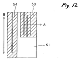
- a known antenna of a one-chip type corresponding to dual band and having a feeder-side radiation electrode 53 and a non-feeder-side radiation electrode 54 that are formed side by side on the top face of a rectangular dielectric substrate 51 such that excitation directions A and B cross at right angles (cf., Japanese Patent Publication No. 2001-7639A, for example).
- the surface area of an antenna tends to become large because two of the radiation electrodes are disposed in parallel on the face side of the dielectric substrate and this results in failing to meet the demands for downsizing.
- the problem in this case is that the electrodes will interfere with each other when the space therebetween is narrow and the adjustment of the resonance frequency on one side affects the matching characteristic and resonance frequency in the other frequency band, thus making the adjustment difficult.
- the space between the radiation electrodes has to be increased to avoid the above isolation problem as much as possible, another problem arising from increasing the space between the two radiation electrodes is that the surface area of the antenna becomes still larger.
- a dielectric antenna comprising:
- the "electromagnetic coupling” includes at least one of coupling by direct joint, capacity coupling and magnetic coupling.
- the first radiation electrode and the second radiation electrode can be arranged on a small body of the dielectric substrate while maintaining a relatively large distance between both radiation electrodes. Since the interference between the radiation electrodes can be made small, it is possible to suppress the affection to the resonance frequencies and the matching characteristics due to the interference.
- both radiation electrodes can be connected to the same feeder electrode. Even if the second radiation electrode is directly connected to the feeder electrode, by narrowing the distance between the power feeding ends, the second radiation electrode can be electrically coupled with the feeder electrode by way of the first radiation electrode. As a result, signals associated with two frequencies can be communicated via the single power feeder while maintaining the independent adjustability for the resonance frequencies and the matching characteristics of the radiation electrodes.
- the first radiation electrode extends parallel to at least one of the second face and a first one of the side faces.
- the first radiation electrode has a first end which is made open and a second end which is connected to the ground electrode.
- the feeder electrode extends parallel to one of the first one of the side faces and a second one of the side faces.
- the second radiation electrode extends parallel to one of the second one of the side faces.
- the first radiation electrode includes a first section extending parallel to the second face, and a second section extending parallel to at least one of the side faces so as to connect the first section and the grounding electrode.
- the resonance frequency and the matching characteristics of the first radiation electrode can be adjusted by changing the width of the second section.
- the second radiation electrode has a first end which is made open and a second end which is connected to the ground electrode; and the second radiation electrode extends so as to have at least one curved portion. In this case, by narrowing a width of the curved portion, the resonance frequency of the second radiation electrode can be adjusted.
- the second radiation electrode extends in a meandering manner.
- the space dominated by the second radiation electrode can be reduced while maintaining the resonance frequency thereof.
- the area that the first radiation electrode and the second radiation electrode are closely opposed can be reduced. Accordingly, the independent adjustment of the characteristics of the first radiation electrode and the second radiation electrode can be facilitated since the coupling between both of the radiation electrodes becomes weak.
- the first radiation electrode is provided on a first one of the side faces
- the second radiation electrode is provided on a second one of the side faces which opposes to the first one of the side faces.
- the distance between the first radiation electrode and the second radiation electrode is further enlarged, so that the coupling between both of the radiation electrodes becomes weak. Accordingly, the independent adjustment of the characteristics of the first radiation electrode and the second radiation electrode can be facilitated.
- the first radiation electrode and the feeder electrode are directly connected.
- the terminal is provided on the first face while being insulated from the grounding electrode.
- a power feeding section on a circuit board and the terminal can be easily connected by simply mounting the antenna on the circuit board.
- a communication device comprising:
- the data communication described the above can be executed without requiring a space and without changing the arrangement of the conventional circuit board installed in the communication device.
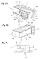
- FIGs. 1A and 1B show a dielectric antenna according to a first embodiment of the invention.
- a first radiation electrode 2 for use mainly in a first frequency band f 1 is provided as a conductive film formed on a dielectric substrate 1.
- One end 21 of the first radiation electrode 2 is provided as an open end on a top face 11 of the dielectric substrate 1.
- the first radiation electrode 2 is extended by way of the top face 11 and a side face 12 and connected to a grounding electrode 5 formed on a bottom face 16 opposing to the top face 11.
- the longitudinal dimension (L 1 +L 2 ) from the one end 21 to the other end 22 of the radiation electrode 2 is set equal to an electrical length of approximately 1/4 of the wavelength of the desired first frequency band ( ⁇ 1 ).
- this physical length is inversely proportional to the square root of the relative dielectric constant ⁇ r of the dielectric substrate 1 (proportional to ⁇ r -1/2 ), the physical length can be shortened as described above by using a dielectric substrate 1 having a greater dielectric constant.
- the dielectric substrate 1 is desirably made of ordinary ceramics having a relative dielectric constant of about 8, for example, may be used though ceramics such as BaO-TiO 2 -SnO 2 , MgO-CaO-TiO 2 or the like is preferred in point of downsizing as the relative dielectric constant becomes about 20 or greater. Further, the dielectric substrate 1 may be formed integrally of dielectric material such as ceramics, formed by laminating and sintering thin ceramic sheets provided with proper conductive films thereon or formed by laminating glass epoxy films provided with proper conductive films.
- the width W of the first radiation electrode 2 is set substantially equal to the width of the dielectric substrate 1. The greater the width W of the radiation electrode 1, the wider the band characteristics become, which is desirable.
- the first radiation electrode 2 is formed over a first side face 12 from the top face 11 but also side radiation electrodes 23 and 24 are formed on the second side face 13 and the third side face 14 that are adjacent to the first side face 12.
- the side radiation electrode 23 formed on the second side face 13 is connected to a feeder electrode 3 (described later), while the side radiation electrode 24 formed on the third side face 14 is directly connected to the grounding electrode 5.
- the resonance frequencies of side radiation electrodes 23 and 24 formed on the respective second and third side faces 13 and 14 are lowered by narrowing their width "d" and when their resonance frequencies change under the influence of the second radiation electrode 4, which will be described later, the side radiation electrodes 23 and 24 are subjected to adjustment by changing the width of the side radiation electrodes 23 and 24.
- the radiation electrode 2 is not limited in configuration to the example shown above but may be provided on any one of the side faces other than the top face unless close coupling is established between the radiation electrode 2 and the second radiation electrode 4.
- the feeder electrode 3 is directly connected to the first radiation electrode 2.
- the wider portion is defined as a part of the first radiation electrode 2 (the side radiation electrode 23) and the narrower portion is defined as the feeder electrode 3 herein for convenience.
- the width of the feeder electrode 3 may be coincident with that of the side radiation electrode 23, or it may cause the entire part of the electrode formed on the second side face 13 to serve as the feeder electrode 3.
- the feeder electrode 3 is connected to a portion of the radiation electrode 2, having a predetermined impedance to form an inverted-F antenna.
- the end portion of the feeder electrode 3 is made the feeder terminal 31 provided separately from the grounding electrode 5 as shown in Fig. 1 B. When the end portion thereof is mounted onto a circuit board (not shown), it is directly connected to the feeder portion of the circuit board by soldering.
- the feeder electrode 3 is provided in various places as will be described later.
- a second radiation electrode 4 is a radiation electrode for use mainly in the second frequency band f 2 and is formed on the second side face 13 of the dielectric substrate 1, so that it is electromagnetically coupled with the feeder electrode 3 and/or the first radiation electrode 2 and resonated in the second frequency band.
- the second radiation electrode 4 is formed closer to the feeder electrode 3 so that it is coupled with the feeder electrode 3 more strongly; in other words, the second radiation electrode 4 is formed so that it is weakly coupled with the main part of the first radiation electrode 2 formed on the top face 11 of the dielectric substrate 1 whereby to increase the distance B between the second radiation electrode 4 and the first radiation electrode 2 as much as possible.
- the second radiation electrode 4 is formed such that it is extended in the longitudinal direction and bent toward the grounding electrode 5 with its length L 3 being equal to an electrical length of approximately 1/4 of the wavelength of the second frequency band ( ⁇ 2 ). Even in this case, further, the resonance frequency can be lowered by scraping a bent portion 41 so as to reduce width "h” whereby to increase L 3 .
- the resonance frequency and matching characteristic are caused to change by coupling the second radiation electrode 4 with the first radiation electrode 2, the adjustment can be made by changing the width "h" of the bent portion 41.
- the second radiation electrode 4 may be formed from the second side face 13 to a fourth side face 15 opposing the first side face 12 or may be in a meandering form as will be described later. With the second radiation electrode 4 formed on the third side face 14, the second radiation electrode 4 may be formed so that it is coupled with the feeder electrode 3 via the first radiation electrode 2 without being directly coupled with the feeder electrode 3.
- the grounding electrode 5 is provided over the substantially whole bottom face 16 excluding a portion where the feeder terminal 31 is provided. Part of the grounding electrode 5 is partly continued to the second and third side faces 13, 14 as a fixing terminal 51.
- the grounding electrode 5 is mounted onto a circuit board (not shown), it is fixed to the earth-line of the circuit board by soldering, whereby the fixation of the antenna and the electrical connection of the grounding electrode 5 can be conducted simultaneously.
- the grounding electrode 5, the first and second radiation electrodes 2 and 4, the feeder electrode 3 and so forth in position on the dielectric substrate 1 by printing conductive films such as silver films or vacuum plating and patterning is preferred because these component parts are formable with ease
- the way to form them is not limited to this example but may include a structure in which conductive lines or plates made of copper are provided in prescribed locations on the dielectric substrate 1.
- a belt-shaped via contact is formed on each of the dielectric sheets and by laminating the sheets whereby to form a conductive film in the vertical direction and the dielectric film is provided on the side after the formation of a laminated dielectric sheet body so as to form an electrode.
- an electrode can be formed inside by covering the face with the dielectric sheet.
- the first radiation electrode 2 so configured as described the above serves as an inverted-F antenna as shown by an equivalent circuit diagram in Fig. 1 C.
- the second radiation electrode 4 is electromagnetically coupled with the feeder electrode 3, that is, the feeder terminal 31 by the distance A with respect to the feeder electrode 3 and the distance B with respect to the first radiation electrode 2.
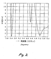
- the resonance frequencies and matching characteristics of the first and second radiation electrodes 2 and 4 change, depending on the degree of coupling the second radiation electrode 4 with the feeder electrode 3 as well as the first radiation electrode 2 and by setting the distances A and B so that both of them are optimized, the resonance frequencies and matching characteristics in the dual band can be adjusted.
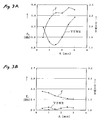
- FIGs. 3A and 3B show the results of examining variations in the resonance frequencies and VSWR in the 2.4 GHz and 5.2 GHz bands when the distance A is varied while the distance B is kept at 2 mm.
- the distance A was varied by scraping the side end portion of the feeder electrode 3 as described above.
- almost no change of VSWR is seen in the 2.4 GHz band and the best result is seen when the distance A is 1.5 mm in the 5.2 GHz band.
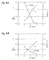
- Figs. 4A and 4B show the results of examining variations in the resonance frequencies and VSWRs in the 2.4 GHz and 5.2 GHz bands when only the distance B is varied while the distance A is kept at 1.5 mm.
- the distance B was changed by scraping the upper end portion of the second radiation electrode 4 so as to gradually enlarge the space with the first radiation electrode 2.
- good results are seen to be obtainable in both the 2.4 GHz and 5.2 GHz bands when the distance B is enlarged.
- the first radiation electrode 2 is formed such that the one end 21 is provided as an open end on the end portion of the top face 11 of the dielectric substrate 1; the other end 22 is extended along the longitudinal direction on the top face 11 of the dielectric substrate 1 and connected to the grounding electrode 5 via the first side face 12; and the feeder electrode 3 is connected to the first radiation electrode 2 in a portion close to the other end 22 having the predetermined impedance to form the inverted-F antenna as shown in the equivalent circuit diagram of Fig. 1 C.
- the second radiation electrode 4 is formed on the second side face 13 in an extended condition in the longitudinal direction of the side of the dielectric substrate 1 as well.
- the first radiation electrode 2 and the second radiation electrode 4 are coupled with each other to no small extent and mutually affect each other.
- the space between the radiation electrodes thus coupled together grows larger. Consequently, the frequencies and the VSWRs slightly change as shown in Figs. 3A through 4B, whereupon the resonance frequencies and the VSWRs of both the radiation electrodes 2 and 4 are made adjustable independently from each other by adjusting the width of the side radiation electrode 23 or the side radiation electrode 24 provided on the second side face 13 or the third side face 14 of the first radiation electrode 2 and changing the width of the vertical portion of the second radiation electrode 4.
- Fig. 5 shows a second embodiment of the invention. Similar components to those in the first embodiment will be designated by the same reference number and the repetitive explanation for those will be omitted.
- the first radiation electrode 2 is extended up to the fourth side face 15 so that the open end 21 is provided on the fourth side face 15.
- the length L 5 of the dielectric substrate 1 can be shortened because it is only needed for the sum of the length L 4 of the first radiation electrode 2 in the portion of the fourth side face 15, the longitudinal dimension L 5 of the dielectric substrate 1 and the length L 2 of the first side face 12 (L 4 + L 5 + L 2 ) to become equivalent to the electrical length of ⁇ 1 /4, so that the downsizing of the antenna is attemptable.
- Figs. 6A and 6B show a third embodiment of the invention. Similar components to those in the first embodiment will be designated by the same reference number and the repetitive explanation for those will be omitted.
- the other end 22 of the first radiation electrode 2 is connected to the grounding electrode 5 via the first side face 12 and part of the radiation electrode 2 on the first side face 12 is not connected to the grounding electrode 5 but connected to the feeder electrode 3. More specifically, a part of the radiation electrode 2 closer the second side face 13 is not connected to the grounding electrode 5 but connected to the feeder electrode 3 formed on the first side face 12 and the rest part of the radiation electrode 2 is connected to the grounding electrode 5. Consequently, the structure of the combination of the radiation electrode 2 and the coupling electrode 3 is similar to the aforementioned structure.
- this structure is made to operate as the inverted-F antenna as in the aforementioned embodiments by setting the distance between the joint of the radiation electrode 2 toward the grounding electrode 5 and the feeder electrode 3 so that the node between the feeder electrode 3 and the radiation electrode 2 is located at a position having the predetermined impedance.
- the feeder electrode 3 and the second radiation electrode 4 are not formed on the same face, the feeder electrode 3 and the second radiation electrode 4 are strongly coupled together by the magnetic field, so that both of them can substantially be coupled as well if the distance therebetween is close.
- the feeder terminal 31 is formed on the bottom face 16 at a position closer to the first side face 12 and surrounded with the grounding electrode 5. This structure is allowed to deal with a case where power cannot be supplied from the side of the second side face 13 or the third side face 14.
- Fig. 7 shows a fourth embodiment of the invention. Similar components to those in the first embodiment will be designated by the same reference number and the repetitive explanation for those will be omitted.
- the side radiation electrode 24 is removed from the structure of the third embodiment.
- the resonance frequency and the VSWR are changed by the coupling between the first radiation electrode and the second radiation electrode, such changes can be adjusted by providing the side radiation electrode 24 and changing the width thereof.
- the design adjusted once the same frequency and VSWR characteristics are obtainable from the same structure manufactured and when the adjustment of impedance changing due to a circuit board is completed, that circuit board can be formed in a prescribed configuration. Therefore, the side radiation electrode becomes unnecessary on condition that the adjustment above can be conducted without the side radiation electrode.
- the length of the portion of the radiation electrode can be increased, the portion thereof being not connected to the grounding electrode 5, the length L in the longitudinal direction of the dielectric substrate 1 can be decreased, so that the downsizing of the antenna is attemptable.
- This configuration is applicable to all the embodiments as described the above.
- FIGs. 8 and 9 show fifth and sixth embodiments of the invention. Similar components to those in the first embodiment will be designated by the same reference number and the repetitive explanation for those will be omitted.
- the second radiation electrode 4 is extended in a meandering manner (cranked or curved). With this configuration, it is possible to shorten the physical length L 6 in the longitudinal direction to obtain the required electrical length (1/4 of the wavelength of the resonance frequency). Consequently, the meandering form is readily provided on the second side face 13 in case that it is necessary to increase the length of the second radiation electrode 4 when the second frequency band is relatively low.
- the whole length L 6 in the longitudinal direction of the second radiation electrode 4 is made shorter by forming the second radiation electrode 4 in the meandering manner, the length of the portion of the second radiation electrode 4 opposing to the first radiation electrode 2 on the top face 11 can be shortened, so that the capacity is made smaller and also the degree of coupling between both the radiation electrodes is lowered. Therefore, the same effect as what makes the distance B between the radiation electrodes 2 and 4 shown in Fig. 1 A greater. Moreover, since the space between both the radiation electrodes is caused to become smaller and greater periodically, the capacity of a receding portion 44 is decreased further, so that the degree of coupling between the radiation electrodes as a whole can be lowered. In this case, the first radiation electrode 2 or both the radiation electrodes may be formed in the meandering manner. This structure is applicable to each of the aforementioned embodiments.
- Fig. 10 shows a seventh embodiment of the invention. Similar components to those in the first embodiment will be designated by the same reference number and the repetitive explanation for those will be omitted.
- the first radiation electrode 2 is provided so as to extend from the third side face 14 to the second side face 13 via the first side face 11 and is connected to the feeder electrode 3 formed on the second side face 13.
- a part of the first radiation electrode 2 formed on the first side face 12 is connected to the grounding electrode 5. Consequently, the feeder electrode 3 is formed in a position where the impedance becomes a predetermined value apart by a predetermined distance from the portion where the radiation electrode 2 is connected to the grounding electrode 5, whereby an inverted-F antenna can be formed as in each of the aforementioned embodiments.
- the length of the whole portion of the first radiation electrode 2 extended linearly is needless to say adjusted so that the resonance is triggered in the first frequency band f 1 .
- the feeder electrode 3 is electromagnetically coupled with the first radiation electrode 2 and the second radiation electrode 4 and one antenna is allowed to deal with dual band.
- the distance therebetween can be enlarged, whereas both of them are coupled less intimately, whereby the resonance frequency and matching characteristic of each can be adjusted independently.
- the top face 11 is set free from being used for printing the conductive film so as to form an electrode, one manufacturing step can be omitted.
- the first radiation electrode 2 is formed over the whole width of the top face 11 of the dielectric substrate 1.
- the width of the radiation electrode 2 may be smaller than the width of the whole width of the top face 11. In such a case, the space between the first radiation electrode 2 and the second radiation electrode 4 is enlarged and this is preferable in that both the radiation electrodes are weakly coupled together.
- the second radiation electrode 4 is provided near the feeder electrode 3 so that the second radiation electrode 2 is directly coupled with the feeder electrode 3.
- the second radiation electrode 4 may be formed on the third side face 14 opposing the second side face 13.
- the second radiation electrode 4 and the first radiation electrode 2 are disposed close to each other whereby to couple the second radiation electrode 4 with the feeder electrode 3 via the first radiation electrode 2.
- the first radiation electrode 2 renders a contribution to the second frequency band, there arises a complicated problem from the relevancy of the resonance frequency and VSWR to the first radiation electrode.
- Fig. 11 shows an example of a personal computer loaded with an antenna for use in forming LAN.
- An antenna 7 is mounted inside the side wall 61 of a personal computer 6 and connected to a communication circuit (not shown) provided inside the personal computer 6, so that radio communication is carried out with any other personal computer, cellular phone or the like having the same communication functions.
- the antenna 7 is disposed such that the second radiation electrode 4 faces upward.
- the place of mounting the antenna 7 is not limited to a position indicated in Fig. 11 but may be on the other side, the back side of the personal computer 6 or in a cover portion 62.
- the grounding electrode of the antenna 7 may be mounted by soldering in the upper corner of a built-in circuit board of the cellular phone with the fixing terminal 51 above.
Landscapes
- Engineering & Computer Science (AREA)
- Computer Networks & Wireless Communication (AREA)
- Details Of Aerials (AREA)
- Waveguide Aerials (AREA)
- Support Of Aerials (AREA)
Applications Claiming Priority (2)
| Application Number | Priority Date | Filing Date | Title |
|---|---|---|---|
| JP2003405515 | 2003-12-04 | ||
| JP2003405515A JP4189306B2 (ja) | 2003-12-04 | 2003-12-04 | 誘電体アンテナおよびそれを用いた通信機能を有する電気機器 |
Publications (1)
| Publication Number | Publication Date |
|---|---|
| EP1538701A1 true EP1538701A1 (de) | 2005-06-08 |
Family
ID=34463991
Family Applications (1)
| Application Number | Title | Priority Date | Filing Date |
|---|---|---|---|
| EP04028673A Withdrawn EP1538701A1 (de) | 2003-12-04 | 2004-12-03 | Dielektrische Antenne und Kommunikationsvorrichtung mit derselben |
Country Status (6)
| Country | Link |
|---|---|
| US (1) | US7196664B2 (de) |
| EP (1) | EP1538701A1 (de) |
| JP (1) | JP4189306B2 (de) |
| KR (1) | KR20050054478A (de) |
| CN (1) | CN100585944C (de) |
| TW (1) | TW200537740A (de) |
Cited By (3)
| Publication number | Priority date | Publication date | Assignee | Title |
|---|---|---|---|---|
| WO2006114668A1 (en) * | 2005-04-26 | 2006-11-02 | Nokia Corporation | Dual-layer antenna and method |
| EP1903633A1 (de) * | 2006-09-25 | 2008-03-26 | Samsung Electronics Co., Ltd. | Eingebaute Antenne für ein tragbares Endgerät |
| US8159400B2 (en) | 2007-07-12 | 2012-04-17 | Samsung Electro-Mechanics Co., Ltd. | Chip antenna and mobile-communication terminal having the same |
Families Citing this family (33)
| Publication number | Priority date | Publication date | Assignee | Title |
|---|---|---|---|---|
| WO2006134701A1 (ja) * | 2005-06-17 | 2006-12-21 | Murata Manufacturing Co., Ltd. | アンテナ装置及び無線通信機 |
| US7170433B1 (en) * | 2005-06-20 | 2007-01-30 | The Mathworks, Inc. | Analog I/O board providing analog-to-digital conversion and having a two-level buffer that allows demand based access to converted data |
| KR100799844B1 (ko) * | 2006-03-14 | 2008-01-31 | 삼성전기주식회사 | 복수의 급전부를 구비한 내장형 안테나 |
| US7450072B2 (en) * | 2006-03-28 | 2008-11-11 | Qualcomm Incorporated | Modified inverted-F antenna for wireless communication |
| JP4100460B2 (ja) * | 2006-05-11 | 2008-06-11 | 株式会社村田製作所 | アンテナ装置およびそれを用いた無線通信装置 |
| KR100814432B1 (ko) | 2006-08-29 | 2008-03-18 | 삼성전자주식회사 | Sar이 감소된 이중대역 역 f안테나 |
| KR100856310B1 (ko) * | 2007-02-28 | 2008-09-03 | 삼성전기주식회사 | 이동통신 단말기 |
| US7705787B2 (en) * | 2007-03-26 | 2010-04-27 | Motorola, Inc. | Coupled slot probe antenna |
| US7733277B2 (en) * | 2007-07-24 | 2010-06-08 | Cheng Uei Precision Industry Co., Ltd. | Wide band antenna |
| US7629933B2 (en) * | 2007-08-23 | 2009-12-08 | Research In Motion Limited | Multi-band antenna, and associated methodology, for a radio communication device |
| US8618988B2 (en) * | 2007-10-05 | 2013-12-31 | Kyocera Corporation | Co-location insensitive multi-band antenna |
| KR101349519B1 (ko) * | 2007-11-21 | 2014-01-08 | 엘지이노텍 주식회사 | 안테나 |
| KR100939478B1 (ko) | 2008-01-04 | 2010-01-29 | (주)광진텔레콤 | 마이크로 평면 역 지 칩 안테나 |
| KR100862493B1 (ko) | 2008-06-25 | 2008-10-08 | 삼성전기주식회사 | 이동통신 단말기 |
| TW201021293A (en) * | 2008-08-12 | 2010-06-01 | Kantatsu Co Ltd | Chip antenna |
| CN101728624B (zh) * | 2008-10-10 | 2013-11-06 | 智易科技股份有限公司 | 天线的馈入结构 |
| JP4951028B2 (ja) | 2009-05-28 | 2012-06-13 | 株式会社日本自動車部品総合研究所 | 車載アンテナ装置 |
| KR101077452B1 (ko) | 2009-08-19 | 2011-10-26 | 엘지이노텍 주식회사 | 무선 통신모듈 |
| JP2011077714A (ja) * | 2009-09-29 | 2011-04-14 | Tdk Corp | 複共振アンテナ及び通信装置 |
| JP5494310B2 (ja) * | 2010-06-22 | 2014-05-14 | Tdk株式会社 | アンテナ装置 |
| JP2012109875A (ja) * | 2010-11-18 | 2012-06-07 | Fujitsu Ltd | アンテナ装置及び無線通信装置 |
| CN102856634B (zh) * | 2012-09-20 | 2016-02-24 | 上海安费诺永亿通讯电子有限公司 | 一种适用于笔记本或平板电脑的新型宽带lte天线 |
| CN102969563B (zh) * | 2012-11-20 | 2015-12-02 | 青岛歌尔声学科技有限公司 | 一种双频带天线及其制作方法 |
| KR101470117B1 (ko) * | 2013-01-25 | 2014-12-05 | 엘지이노텍 주식회사 | 안테나 장치 |
| CN105849974B (zh) * | 2014-01-20 | 2019-03-01 | Agc株式会社 | 天线装置以及具备该天线装置的无线装置 |
| WO2017122851A1 (ko) * | 2016-01-15 | 2017-07-20 | 주식회사 갤트로닉스 코리아 | 금속 재질의 디바이스에 적용 가능한 입체 피파 커플링 안테나 |
| JP6881593B2 (ja) * | 2017-10-30 | 2021-06-02 | 株式会社村田製作所 | アンテナ装置および通信装置 |
| KR102327550B1 (ko) | 2018-03-06 | 2021-11-16 | 동우 화인켐 주식회사 | 필름 안테나 및 이를 포함하는 디스플레이 장치 |
| KR102049755B1 (ko) * | 2018-07-27 | 2019-11-28 | 주식회사 에이스테크놀로지 | 버튼 장치를 이용한 다중 대역 안테나 및 통신 단말기 |
| DE102019205556A1 (de) | 2019-04-17 | 2020-10-22 | BSH Hausgeräte GmbH | Leiterplatten-Antenne |
| JP7369919B2 (ja) | 2020-02-13 | 2023-10-27 | パナソニックIpマネジメント株式会社 | アンテナ装置 |
| CN116345156A (zh) * | 2023-01-16 | 2023-06-27 | 环鸿电子(昆山)有限公司 | 天线结构及电子装置 |
| TWI881454B (zh) * | 2023-09-06 | 2025-04-21 | 萬誠科技股份有限公司 | 天線結構 |
Citations (5)
| Publication number | Priority date | Publication date | Assignee | Title |
|---|---|---|---|---|
| EP1122812A2 (de) * | 2000-02-04 | 2001-08-08 | Murata Manufacturing Co., Ltd. | Oberflächenmontierte Antenne und Kommunikationsvorrichtung mit einer derartigen Antenne |
| JP2002118418A (ja) * | 2000-10-04 | 2002-04-19 | Murata Mfg Co Ltd | 表面実装型アンテナおよびアンテナの実装構造および無線装置 |
| JP2002158529A (ja) * | 2000-11-20 | 2002-05-31 | Murata Mfg Co Ltd | 表面実装型アンテナ構造およびそれを備えた通信機 |
| US20020089454A1 (en) * | 2000-10-13 | 2002-07-11 | Steve Eggleston | Antenna transducer assembly, and an associated method therefor |
| WO2004047220A1 (en) * | 2002-11-20 | 2004-06-03 | Nokia Corporation | Controllable antenna arrangement |
Family Cites Families (3)
| Publication number | Priority date | Publication date | Assignee | Title |
|---|---|---|---|---|
| JP2898921B2 (ja) | 1996-06-20 | 1999-06-02 | 株式会社ヨコオ | アンテナおよび無線機 |
| JP3554960B2 (ja) | 1999-06-25 | 2004-08-18 | 株式会社村田製作所 | アンテナ装置およびそれを用いた通信装置 |
| US6384786B2 (en) | 2000-01-13 | 2002-05-07 | Murata Manufacturing Co., Ltd. | Antenna device and communication apparatus |
-
2003
- 2003-12-04 JP JP2003405515A patent/JP4189306B2/ja not_active Expired - Fee Related
-
2004
- 2004-12-02 US US11/001,318 patent/US7196664B2/en not_active Expired - Fee Related
- 2004-12-03 TW TW093137305A patent/TW200537740A/zh unknown
- 2004-12-03 CN CN200410100160A patent/CN100585944C/zh not_active Expired - Fee Related
- 2004-12-03 EP EP04028673A patent/EP1538701A1/de not_active Withdrawn
- 2004-12-04 KR KR1020040101532A patent/KR20050054478A/ko not_active Ceased
Patent Citations (5)
| Publication number | Priority date | Publication date | Assignee | Title |
|---|---|---|---|---|
| EP1122812A2 (de) * | 2000-02-04 | 2001-08-08 | Murata Manufacturing Co., Ltd. | Oberflächenmontierte Antenne und Kommunikationsvorrichtung mit einer derartigen Antenne |
| JP2002118418A (ja) * | 2000-10-04 | 2002-04-19 | Murata Mfg Co Ltd | 表面実装型アンテナおよびアンテナの実装構造および無線装置 |
| US20020089454A1 (en) * | 2000-10-13 | 2002-07-11 | Steve Eggleston | Antenna transducer assembly, and an associated method therefor |
| JP2002158529A (ja) * | 2000-11-20 | 2002-05-31 | Murata Mfg Co Ltd | 表面実装型アンテナ構造およびそれを備えた通信機 |
| WO2004047220A1 (en) * | 2002-11-20 | 2004-06-03 | Nokia Corporation | Controllable antenna arrangement |
Non-Patent Citations (2)
| Title |
|---|
| PATENT ABSTRACTS OF JAPAN vol. 2002, no. 08 5 August 2002 (2002-08-05) * |
| PATENT ABSTRACTS OF JAPAN vol. 2002, no. 09 4 September 2002 (2002-09-04) * |
Cited By (4)
| Publication number | Priority date | Publication date | Assignee | Title |
|---|---|---|---|---|
| WO2006114668A1 (en) * | 2005-04-26 | 2006-11-02 | Nokia Corporation | Dual-layer antenna and method |
| US7183983B2 (en) | 2005-04-26 | 2007-02-27 | Nokia Corporation | Dual-layer antenna and method |
| EP1903633A1 (de) * | 2006-09-25 | 2008-03-26 | Samsung Electronics Co., Ltd. | Eingebaute Antenne für ein tragbares Endgerät |
| US8159400B2 (en) | 2007-07-12 | 2012-04-17 | Samsung Electro-Mechanics Co., Ltd. | Chip antenna and mobile-communication terminal having the same |
Also Published As
| Publication number | Publication date |
|---|---|
| CN1624976A (zh) | 2005-06-08 |
| US7196664B2 (en) | 2007-03-27 |
| JP2005167762A (ja) | 2005-06-23 |
| KR20050054478A (ko) | 2005-06-10 |
| JP4189306B2 (ja) | 2008-12-03 |
| CN100585944C (zh) | 2010-01-27 |
| US20050134510A1 (en) | 2005-06-23 |
| TW200537740A (en) | 2005-11-16 |
Similar Documents
| Publication | Publication Date | Title |
|---|---|---|
| US7196664B2 (en) | Dielectric antenna and communication device incorporating the same | |
| JP4423809B2 (ja) | 複共振アンテナ | |
| EP1248316B1 (de) | Antenne und Kommunikationsgerät mit dieser Antenne | |
| US6218992B1 (en) | Compact, broadband inverted-F antennas with conductive elements and wireless communicators incorporating same | |
| US6424300B1 (en) | Notch antennas and wireless communicators incorporating same | |
| US8686902B2 (en) | Antenna structures | |
| US6268831B1 (en) | Inverted-f antennas with multiple planar radiating elements and wireless communicators incorporating same | |
| US9887465B2 (en) | Single-layer metalization and via-less metamaterial structures | |
| US7602343B2 (en) | Antenna | |
| CN102044738B (zh) | 具有机械连接的超材料天线 | |
| JP2004088218A (ja) | 平面アンテナ | |
| US20090135087A1 (en) | Metamaterial Structures with Multilayer Metallization and Via | |
| US6229487B1 (en) | Inverted-F antennas having non-linear conductive elements and wireless communicators incorporating the same | |
| WO2002089249A1 (en) | Broad-band antenna for mobile communication | |
| JPH09219610A (ja) | 表面実装型アンテナおよびこれを用いた通信機 | |
| JP2007089234A (ja) | アンテナ | |
| WO2010033865A2 (en) | Metamaterial loaded antenna devices | |
| JP2003017930A (ja) | アンテナ素子、無線通信装置 | |
| WO2003044891A1 (en) | Dielectric antenna module | |
| JP3921425B2 (ja) | 表面実装型アンテナおよび携帯無線機 | |
| US9024820B2 (en) | Miniature antenna | |
| JPH11340726A (ja) | アンテナ装置 | |
| JP4073789B2 (ja) | 誘電体アンテナ及びそれを内蔵する移動体通信機 | |
| CN101119126A (zh) | 一种无线网卡及其天线 | |
| JP3952385B2 (ja) | 表面実装型アンテナ及びそれを搭載した通信機器 |
Legal Events
| Date | Code | Title | Description |
|---|---|---|---|
| PUAI | Public reference made under article 153(3) epc to a published international application that has entered the european phase |
Free format text: ORIGINAL CODE: 0009012 |
|
| AK | Designated contracting states |
Kind code of ref document: A1 Designated state(s): AT BE BG CH CY CZ DE DK EE ES FI FR GB GR HU IE IS IT LI LT LU MC NL PL PT RO SE SI SK TR |
|
| AX | Request for extension of the european patent |
Extension state: AL BA HR LV MK YU |
|
| 17P | Request for examination filed |
Effective date: 20051005 |
|
| AKX | Designation fees paid |
Designated state(s): AT BE BG CH CY CZ DE DK EE ES FI FR GB GR HU IE IS IT LI LT LU MC NL PL PT RO SE SI SK TR |
|
| STAA | Information on the status of an ep patent application or granted ep patent |
Free format text: STATUS: THE APPLICATION IS DEEMED TO BE WITHDRAWN |
|
| 18D | Application deemed to be withdrawn |
Effective date: 20090224 |