EP1536509B1 - Anordnung zur Variation der Parameter einer elektromagnetischen Welle - Google Patents
Anordnung zur Variation der Parameter einer elektromagnetischen Welle Download PDFInfo
- Publication number
- EP1536509B1 EP1536509B1 EP20040106045 EP04106045A EP1536509B1 EP 1536509 B1 EP1536509 B1 EP 1536509B1 EP 20040106045 EP20040106045 EP 20040106045 EP 04106045 A EP04106045 A EP 04106045A EP 1536509 B1 EP1536509 B1 EP 1536509B1
- Authority
- EP
- European Patent Office
- Prior art keywords
- line
- ferrite
- ferrite layers
- circuit
- structures
- Prior art date
- Legal status (The legal status is an assumption and is not a legal conclusion. Google has not performed a legal analysis and makes no representation as to the accuracy of the status listed.)
- Expired - Lifetime
Links
- 229910000859 α-Fe Inorganic materials 0.000 claims description 29
- 239000000758 substrate Substances 0.000 claims description 10
- 238000004804 winding Methods 0.000 claims description 7
- 238000001465 metallisation Methods 0.000 claims description 6
- 230000001902 propagating effect Effects 0.000 claims 1
- 230000005415 magnetization Effects 0.000 description 18
- 239000004020 conductor Substances 0.000 description 6
- 230000010363 phase shift Effects 0.000 description 6
- 239000000463 material Substances 0.000 description 3
- 238000000034 method Methods 0.000 description 3
- 230000000694 effects Effects 0.000 description 2
- 238000005516 engineering process Methods 0.000 description 2
- 239000002184 metal Substances 0.000 description 2
- 230000008878 coupling Effects 0.000 description 1
- 238000010168 coupling process Methods 0.000 description 1
- 238000005859 coupling reaction Methods 0.000 description 1
- 230000001419 dependent effect Effects 0.000 description 1
- 238000010586 diagram Methods 0.000 description 1
- 238000004519 manufacturing process Methods 0.000 description 1
- 230000000644 propagated effect Effects 0.000 description 1
- 238000005245 sintering Methods 0.000 description 1
- 229910052566 spinel group Inorganic materials 0.000 description 1
Images


Classifications
-
- H—ELECTRICITY
- H01—ELECTRIC ELEMENTS
- H01P—WAVEGUIDES; RESONATORS, LINES, OR OTHER DEVICES OF THE WAVEGUIDE TYPE
- H01P1/00—Auxiliary devices
- H01P1/18—Phase-shifters
- H01P1/19—Phase-shifters using a ferromagnetic device
-
- H—ELECTRICITY
- H01—ELECTRIC ELEMENTS
- H01P—WAVEGUIDES; RESONATORS, LINES, OR OTHER DEVICES OF THE WAVEGUIDE TYPE
- H01P1/00—Auxiliary devices
- H01P1/22—Attenuating devices
- H01P1/23—Attenuating devices using ferromagnetic material
Definitions
- the invention relates to a device for varying at least one component or parameter of an electromagnetic wave.
- It relates, for example, a ferrite phase shifter, or a microwave attenuator.
- the U.S. Patent 5,774,025 discloses a method of manufacturing a planar phase shifter composed of several layers of ferrite.
- the layers are metallized by applying a quantity of conductive metal according to a selected diagram.
- Metallic orifices ensure the connection of the layers together.
- the assembly is then brought to a temperature of between 800 ° C. and 1000 ° C. in order to obtain an integrated structure.
- triplate line that deploys within the volume of the material in order to obtain a sufficient length by which it is possible to vary a component of the electromagnetic wave a specific phase shift may be feasible .
- triplaque line or mean a line that consists of a central ribbon placed between two ground planes.
- the object of the invention relates to a device for varying one or more parameters of a microwave wave.
- the invention notably offers the possibility of producing an extremely integrated phase shifter. It also makes it possible to obtain a device fulfilling the attenuator function and / or the phase shifter function in a restricted volume.
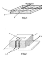
- the figure 1 schematizes the principle used in the device according to the invention where the propagation line 2 of the microwave waves is a triplate line whose substrate 1 is a ferrite material.
- the width of the line and the thickness of the circuit thus formed are adjusted for example so as to obtain an impedance of 50 ohms.
- Reference 3 denotes metallization.
- a reciprocal phase shift effect is obtained in the line. This phase shift is related to the intensity of the magnetization.
- one or more parameters of the wave will be varied, for example to obtain an attenuation effect of the wave.
- triplate line allows the realization of a multilayer by stacking the triplate lines on each other. It is sufficient to make an interconnection between the lines by means of metallized holes which connect the central conductors to each other. By employing this method, it is possible to stack several triplate lines on each other and thus obtain a significant electrical length disposed in a volumic circuit. Similarly, on the same circuit layer, the triplate line can be wound so as to maximize its length for a given ferrite surface.
- the winding structure of the triplate line may be a spiral winding, or any other winding geometry for varying, for example, the phase, the amplitude, or any other parameter of the microwave wave.
- the figure 2 represents an external view of a phase-shifting circuit according to the invention. It comprises several layers of substrate 1 stacked on top of each other. These layers consist of ferrite. In the center of the circuit thus formed, there is an orifice 4 for winding a solenoid 5 having in particular the magnetization function of the phase shifter circuit.
- the lines of the solenoids are wound around one of the sides of the device, and comprise two ports 6, 7 respectively for the incoming magnetization current and for the outgoing magnetization current.
- the ferrite which serves as a substrate for the triplate line can also be used as low frequency ferrite for the magnetization circuit. It is also possible to construct the multilayer circuit so that the low-frequency circuit has the form of a closed magnetic core and thus the phase-shifter can be operated by magnetization of the ferrite at the remanence (latched phase shifter).
- metallizing the outer surface of the multilayer circuit for example, turns of the solenoid which constitutes the magnetization circuit.
- the metallization is carried out using a technique known to those skilled in the art.
- the figure 3A is a top view of the upper layer of the circuit.
- This layer is formed of a ferrite substrate 1.
- the turns of the solenoid 5 are wound.
- the figure 3B schematizes the second layer comprising a central conductor of the triplate line.
- This line is distributed spirally around the orifice 4.
- An input 9 of this line is the input of the microwave signal.
- the second layer comprises a metallized hole 8 allowing the propagation of the microwave between the different levels.
- the spacing between the parts constituting the triplate line is chosen so as to minimize the coupling phenomena.
- the total length of the line is for example fixed according to the phase shift value that one wishes to obtain.
- the figure 3C represents the penultimate layer of substrate which comprises the central conductor of the triplate line. It comprises an output 10 for the microwave signal and a metallized hole 8 allowing the passage of the signal to the other levels.
- the 3D figure represents the lower layer of the circuit according to the invention.
- Magnetic solenoid turns winding around one side of the circuit thus formed.
- the microwave signal is thus propagated in the volume of the circuit through the triplate line.
- the figure 4 is a sectional view of a phase shifter according to the invention. This view shows the stack of the different ferrite layers, the metallized holes 8 allowing the connection between the different levels or layers, the central conductor 2 and the metallization 3.
- the thickness of a ferrite layer is 0.15 mm as a standard (method of enclosure).
- a triplate line requires for example 2 layers of ferrite which is 0.33 mm thick with metallization.
- the line can be wound in several turns over a total length of 45mm. In S-band, this length corresponds at least to an electrical length of 2 wavelengths.
- a line of 2 ⁇ per layer of triplate It is considered that it takes between 5 and 10 ⁇ , of total length to create a phase shift of 360 ° (1 ⁇ ), by variation of the magnetization.
- a ferrite multilayer circuit structure is then obtained which contains 6 to 10 layers of ferrite, for a total thickness of 3.3 mm and a surface area of 10 mm by 10 mm.
- the magnetization current to be passed through the solenoid is estimated at some 100 mA, for a time of the order of one ms (5 ⁇ s, ie 5.10 -6 s), by a phase switching.
- Microwave losses are dependent in particular on the technology used, the thickness of the ferrite layers and the width of the central conductors and the quality of the magnetization.
- the ferrite has been used to form the low frequency magnetization toroid of the phase shifter.
- the figure 5 represents an alternative embodiment where the device is an attenuator.
- the ferrite is used to perform another type of magnetization which could move the gyromagnetic resonance close to the frequency band and produce a controllable attenuation. It becomes possible to vary the losses of the circuit and to perform the attenuator function.
- the advantage of such a structure consists in the fact that the same structure of microwave lines arranged in the volume of the ferrite multilayer can be, according to the arrangement of the magnetization metal circuit, used as a phase-shifter or as an attenuator.
- the device of the figure 5 comprises a line allowing the propagation of the microwave waves inside the device, the line being distributed over the different ferrite layers constituting the attenuator / phase shifter circuit as described in FIGS. Figures 3A to 3D . It also comprises a solenoid 5 wound around one side of the circuit allowing the control of phase shifting magnetization and a metallization 11 for example a magnetization control line for the attenuator function.
- Such a structure has the following advantages in particular. In relatively small dimensions, it is possible to obtain the phase-shifter and attenuator functions of an active module, with losses much lower than those of the phase-shifters or attenuators of MMIC technology. Another advantage of this solution lies in the relatively high power handling of this structure, which is estimated at 10 W peaks.
Landscapes
- Waveguide Switches, Polarizers, And Phase Shifters (AREA)
Claims (4)
- Struktur zum Variieren von einem oder mehreren Parametern einer Höchstfrequenzwelle, wobei die Struktur zwei übereinander liegende Ferritlagen (1) und eine auf der Kontaktfläche zwischen den beiden Ferritlagen (1) befindliche elektrische Leitung (2) umfasst, wobei die Baugruppe so angeordnet ist, dass eine Streifenleitung auf einem Ferritsubstrat entsteht, wobei die Außenflächen der Struktur eine Metallisierung (3) aufweisen und die Ferritlagen (1) mit einer Öffnung (4) versehen sind, durch die die Spirale eines Solenoids (5) verläuft, das eine Magnetisierungsschaltung für diese Ferritlagen (1) bildet, wobei die Ferritlagen (1) so ausgelegt sind, dass sie sowohl die Magnetisierungsschaltung als auch das Substrat der Streifenleitung bilden, dadurch gekennzeichnet, dass die Öffnung (4) eine zentrale Öffnung (4) ist und die elektrische Leitung (2) von mehreren Windungen um die zentrale Öffnung (4) gebildet wird.
- Vorrichtung, die mehrere übereinander liegende Strukturen nach Anspruch 1 umfasst, dadurch gekennzeichnet, dass jede Struktur metallisierte Löcher (8) aufweist, die so angeordnet sind, dass die die Strukturen bildenden elektrischen Leitungen paarweise in Kontakt gebracht werden, um eine Streifenleitung zu bilden, die im Wesentlichen das gesamte Volumen der Vorrichtung bildet, wobei ein einziges gemeinsames Solenoid (5) über die Gesamtheit der Strukturen gewunden ist, um die Vorrichtung auf wenigstens einer Seite zu verkapseln.
- Vorrichtung nach Anspruch 2, dadurch gekennzeichnet, dass die Abmessungen der die Strukturen bildenden Ferritlagen (1) so festgelegt sind, dass unter Berücksichtigung der Zahl der auf jeder Struktur realisierten Windungen der elektrischen Leitung die Länge der von der Vorrichtung gebildeten Streifenleitung insgesamt ausreicht, um eine gegebene Phasenverschiebung der sich auf der Leitung ausbreitenden Höchstfrequenzwelle zu erzeugen.
- Vorrichtung nach Anspruch 3, dadurch gekennzeichnet, dass sie ferner eine zweite Magnetisierungsschaltung (11) aufweist mit der Aufgabe, die Amplitude der Höchstfrequenzwelle zu dämpfen.
Applications Claiming Priority (2)
| Application Number | Priority Date | Filing Date | Title |
|---|---|---|---|
| FR0314015 | 2003-11-28 | ||
| FR0314015A FR2863108B1 (fr) | 2003-11-28 | 2003-11-28 | Dispositif permettant la variation des parametres d'une onde electromagnetique |
Publications (2)
| Publication Number | Publication Date |
|---|---|
| EP1536509A1 EP1536509A1 (de) | 2005-06-01 |
| EP1536509B1 true EP1536509B1 (de) | 2010-10-06 |
Family
ID=34451691
Family Applications (1)
| Application Number | Title | Priority Date | Filing Date |
|---|---|---|---|
| EP20040106045 Expired - Lifetime EP1536509B1 (de) | 2003-11-28 | 2004-11-24 | Anordnung zur Variation der Parameter einer elektromagnetischen Welle |
Country Status (3)
| Country | Link |
|---|---|
| EP (1) | EP1536509B1 (de) |
| DE (1) | DE602004029433D1 (de) |
| FR (1) | FR2863108B1 (de) |
Families Citing this family (1)
| Publication number | Priority date | Publication date | Assignee | Title |
|---|---|---|---|---|
| CN104201442B (zh) * | 2014-07-16 | 2016-08-17 | 电子科技大学 | 一种基于ltcc技术的微带线移相器 |
Family Cites Families (6)
| Publication number | Priority date | Publication date | Assignee | Title |
|---|---|---|---|---|
| FR1227407A (fr) * | 1959-03-05 | 1960-08-19 | Csf | Dispositif déphaseur à ferrite |
| US3051917A (en) * | 1960-06-22 | 1962-08-28 | Bell Telephone Labor Inc | Method of suppressing saturation effects in gyromagnetic devices |
| US3332042A (en) * | 1964-09-14 | 1967-07-18 | Ferrite device for effecting reciprocal phase shift or attenuation | |
| US3478283A (en) * | 1967-04-21 | 1969-11-11 | Scientific Atlanta | Reciprocal microwave phase shifter having two magnetizing conductors and one reset conductor |
| JPH0446405A (ja) * | 1990-06-13 | 1992-02-17 | Murata Mfg Co Ltd | ディレイライン及びその製造方法 |
| JPH06334462A (ja) * | 1993-03-26 | 1994-12-02 | Uniden Corp | 超広帯域定位相回路 |
-
2003
- 2003-11-28 FR FR0314015A patent/FR2863108B1/fr not_active Expired - Fee Related
-
2004
- 2004-11-24 EP EP20040106045 patent/EP1536509B1/de not_active Expired - Lifetime
- 2004-11-24 DE DE200460029433 patent/DE602004029433D1/de not_active Expired - Lifetime
Also Published As
| Publication number | Publication date |
|---|---|
| FR2863108A1 (fr) | 2005-06-03 |
| FR2863108B1 (fr) | 2006-02-17 |
| DE602004029433D1 (de) | 2010-11-18 |
| EP1536509A1 (de) | 2005-06-01 |
Similar Documents
| Publication | Publication Date | Title |
|---|---|---|
| EP0123350B1 (de) | Flache Mikrowellenantenne mit einer völlig hängenden Mikrostreifengruppe | |
| EP2795724B1 (de) | Basisantenne und entsprechende ein-oder zweidimensionale gruppenantenne | |
| EP0542595B1 (de) | Mikrostreifenleiterantenne, insbesondere für Fernsprechübertragungen von Satelliten | |
| EP0667984B1 (de) | Monopolantenne mit platten- und stabstrahlern | |
| EP2510574A1 (de) | Mikrowellenübergangsvorrichtung zwischen einer mikrostripleitung und einem rechteckigen wellenleiter | |
| EP3602689B1 (de) | Elektromagnetische antenne | |
| EP1556946B1 (de) | Magnetostatische vorrichtung mit metallischen dünnschichten, herstellungsverfahren und anwendung in vorrichtungen zur verarbeitung von mikrowellensignalen | |
| EP0481417A1 (de) | Vorrichtung zur Speisung eines Strahlungselementes für zwei orthogonale Polarisationen | |
| EP2710676B1 (de) | Strahlerelement für eine aktive gruppenantenne aus elementarfliesen | |
| EP0013222A1 (de) | Diodenphasenschieber für Mikrowellen und elektronisch abtastende Antenne mit einem solchen Schieber | |
| WO2008012369A1 (fr) | Dispositif de transduction orthomode à compacité optimisée dans le plan de maille, pour une antenne | |
| EP1145379A1 (de) | Antenne mit einer filtermaterialanordnung | |
| WO2015177170A1 (fr) | Système d'antennes pour réduire le couplage électromagnétique entre antennes | |
| FR2704357A1 (fr) | Eléments électroniques intégrés à caractéristiques électriques variables, en particulier pour hyperfréquences. | |
| Debogovic et al. | MEMS‐Reconfigurable Metamaterials and Antenna Applications | |
| EP0333567B1 (de) | Mikrowellenschalter | |
| EP1466384A1 (de) | Einrichtung zum empfangen und/oder emittieren elektromagnetischer wellen mit strahlungs-diversity | |
| EP1536509B1 (de) | Anordnung zur Variation der Parameter einer elektromagnetischen Welle | |
| EP1234356A1 (de) | Aktiver hf reflektor unter verwendung von elektronischer strahlschenkung | |
| FR2919432A1 (fr) | Module d'antenne comportant un radome integre. | |
| EP3227960B1 (de) | Selbstkomplementäre mehrschichtige gruppenantenne | |
| EP0335788B1 (de) | Mikrowellenphasenschieber | |
| EP1949496B1 (de) | Flachantennensystem mit direktwellenleiterzugang | |
| FR2519475A1 (fr) | Dispositif selectif accordable a ondes magnetostatiques de volume | |
| Watanabe | A novel polarization-independent beam splitter |
Legal Events
| Date | Code | Title | Description |
|---|---|---|---|
| PUAI | Public reference made under article 153(3) epc to a published international application that has entered the european phase |
Free format text: ORIGINAL CODE: 0009012 |
|
| AK | Designated contracting states |
Kind code of ref document: A1 Designated state(s): AT BE BG CH CY CZ DE DK EE ES FI FR GB GR HU IE IS IT LI LU MC NL PL PT RO SE SI SK TR |
|
| AX | Request for extension of the european patent |
Extension state: AL HR LT LV MK YU |
|
| AKX | Designation fees paid | ||
| 17P | Request for examination filed |
Effective date: 20050812 |
|
| RBV | Designated contracting states (corrected) |
Designated state(s): DE GB IT NL |
|
| REG | Reference to a national code |
Ref country code: DE Ref legal event code: 8566 |
|
| 17Q | First examination report despatched |
Effective date: 20070112 |
|
| GRAP | Despatch of communication of intention to grant a patent |
Free format text: ORIGINAL CODE: EPIDOSNIGR1 |
|
| GRAS | Grant fee paid |
Free format text: ORIGINAL CODE: EPIDOSNIGR3 |
|
| GRAA | (expected) grant |
Free format text: ORIGINAL CODE: 0009210 |
|
| AK | Designated contracting states |
Kind code of ref document: B1 Designated state(s): DE GB IT NL |
|
| REG | Reference to a national code |
Ref country code: GB Ref legal event code: FG4D Free format text: NOT ENGLISH |
|
| REF | Corresponds to: |
Ref document number: 602004029433 Country of ref document: DE Date of ref document: 20101118 Kind code of ref document: P |
|
| REG | Reference to a national code |
Ref country code: NL Ref legal event code: VDEP Effective date: 20101006 |
|
| PG25 | Lapsed in a contracting state [announced via postgrant information from national office to epo] |
Ref country code: NL Free format text: LAPSE BECAUSE OF FAILURE TO SUBMIT A TRANSLATION OF THE DESCRIPTION OR TO PAY THE FEE WITHIN THE PRESCRIBED TIME-LIMIT Effective date: 20101006 |
|
| PLBE | No opposition filed within time limit |
Free format text: ORIGINAL CODE: 0009261 |
|
| STAA | Information on the status of an ep patent application or granted ep patent |
Free format text: STATUS: NO OPPOSITION FILED WITHIN TIME LIMIT |
|
| REG | Reference to a national code |
Ref country code: DE Ref legal event code: R119 Ref document number: 602004029433 Country of ref document: DE Effective date: 20110601 Ref country code: DE Ref legal event code: R119 Ref document number: 602004029433 Country of ref document: DE Effective date: 20110531 |
|
| 26N | No opposition filed |
Effective date: 20110707 |
|
| GBPC | Gb: european patent ceased through non-payment of renewal fee |
Effective date: 20110106 |
|
| PG25 | Lapsed in a contracting state [announced via postgrant information from national office to epo] |
Ref country code: GB Free format text: LAPSE BECAUSE OF NON-PAYMENT OF DUE FEES Effective date: 20110106 |
|
| PG25 | Lapsed in a contracting state [announced via postgrant information from national office to epo] |
Ref country code: IT Free format text: LAPSE BECAUSE OF FAILURE TO SUBMIT A TRANSLATION OF THE DESCRIPTION OR TO PAY THE FEE WITHIN THE PRESCRIBED TIME-LIMIT Effective date: 20101006 |
|
| PG25 | Lapsed in a contracting state [announced via postgrant information from national office to epo] |
Ref country code: DE Free format text: LAPSE BECAUSE OF NON-PAYMENT OF DUE FEES Effective date: 20110531 |