EP0333567B1 - Mikrowellenschalter - Google Patents
Mikrowellenschalter Download PDFInfo
- Publication number
- EP0333567B1 EP0333567B1 EP89400676A EP89400676A EP0333567B1 EP 0333567 B1 EP0333567 B1 EP 0333567B1 EP 89400676 A EP89400676 A EP 89400676A EP 89400676 A EP89400676 A EP 89400676A EP 0333567 B1 EP0333567 B1 EP 0333567B1
- Authority
- EP
- European Patent Office
- Prior art keywords
- branches
- radio frequency
- state
- branch
- switch according
- Prior art date
- Legal status (The legal status is an assumption and is not a legal conclusion. Google has not performed a legal analysis and makes no representation as to the accuracy of the status listed.)
- Expired - Lifetime
Links
Images
Classifications
-
- H—ELECTRICITY
- H01—ELECTRIC ELEMENTS
- H01P—WAVEGUIDES; RESONATORS, LINES, OR OTHER DEVICES OF THE WAVEGUIDE TYPE
- H01P1/00—Auxiliary devices
- H01P1/10—Auxiliary devices for switching or interrupting
-
- H—ELECTRICITY
- H10—SEMICONDUCTOR DEVICES; ELECTRIC SOLID-STATE DEVICES NOT OTHERWISE PROVIDED FOR
- H10N—ELECTRIC SOLID-STATE DEVICES NOT OTHERWISE PROVIDED FOR
- H10N60/00—Superconducting devices
- H10N60/30—Devices switchable between superconducting and normal states
- H10N60/35—Cryotrons
-
- Y—GENERAL TAGGING OF NEW TECHNOLOGICAL DEVELOPMENTS; GENERAL TAGGING OF CROSS-SECTIONAL TECHNOLOGIES SPANNING OVER SEVERAL SECTIONS OF THE IPC; TECHNICAL SUBJECTS COVERED BY FORMER USPC CROSS-REFERENCE ART COLLECTIONS [XRACs] AND DIGESTS
- Y10—TECHNICAL SUBJECTS COVERED BY FORMER USPC
- Y10S—TECHNICAL SUBJECTS COVERED BY FORMER USPC CROSS-REFERENCE ART COLLECTIONS [XRACs] AND DIGESTS
- Y10S505/00—Superconductor technology: apparatus, material, process
- Y10S505/825—Apparatus per se, device per se, or process of making or operating same
- Y10S505/866—Wave transmission line, network, waveguide, or microwave storage device
Definitions
- the subject of the invention is a microwave switch comprising an interference device, one and / or the other branch of which is capable of undergoing a reversible transition from a normal state to a superconductive state, the position of the switch being function of the respective state (normal or superconductor) of the two branches.
- a microwave switch can be advantageously applied to the production of radar system duplexers, microwave phase shifters and microwave attenuators.
- a PIN diode (known to be suitable for microwave signals) as a microwave switch: subject to direct polarization, it behaves like a passing switch, and when it is applied reverse polarization, it is analogous to a switch blocked.
- the time switching of such a diode is limited below by the time necessary for the evacuation of minority carriers (which are the carriers contributing most to the passage of a microwave current when the diode is polarized in the forward direction).
- a PIN diode mounted on a microwave line introduces a parasitic series resistance (phenomenon known to those skilled in the art).
- the power handling of such a diode is limited above by the value of the avalanche voltage of the diode.
- Document DE-A-1 591 528 describes a microwave switch comprising an interference device, one branch of which, containing a ferrite, is capable of undergoing a reversible transition from a normal state to a magnetized state introducing an additional phase shift of ⁇ for the wave crossing it.
- the invention relates to a microwave switch comprising a section of microwave line separating into two branches of different lengths, these two branches then meeting in a second section; the difference in length of the two branches is substantially equal to an odd number of half-wavelengths of operation of the switch; at least one of the two branches is capable of passing reversibly and controlled from a normal state to a superconductive state; the switch is open (that is to say in the blocked state) when the two branches are in the same state, and closed (that is to say in the on state) otherwise.
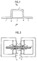
- FIG. 1 represents a partial top view of a switch, according to an embodiment of the invention, manufactured from microstrip lines 1, 2, 3, and 4 having a common dielectric substrate (not shown in FIG. 1 ) and a common ground plane (not shown in Figure 1).
- a first microstrip line 1 (called first section in the following) separates into two microstrip lines 2 and 3 (called branches 2 and 3 in the following) at a bifurcation 23; the two branches 2 and 3 meet at a meeting 32 to reform a single microstrip line 4 (called section 4 in the following).
- the length of the branch 3 is greater than that of the branch 2 and the difference in length between these two branches is substantially equal to an odd number of operating half-wavelengths of the switch.
- the respective central conductors of sections 1 and 4 and branches 2 and 3 are made of the same superconductive material, the critical temperature T c (that is to say the reversible transition temperature between a "normal” state and a state "superconductor” of said material) is preferably greater than 30 K; by way of example, superconductive materials are known whose critical temperature T c is between 30 K and 95 K: these are for example copper oxides.
- the operation of the switch (described below) only involves superconductivity of one or two branches 2 or 3, but the central conductors of the four sections 1 and 4 or branches 2 and 3 are advantageously made from of the same material to avoid the appearance of losses, in particular by reflection at the junctions between different materials, and to simplify the industrial production of the switch object of the present invention.
- the common ground plane (not shown in Figure 1) is preferably made of the same material as the central conductors, and this for convenience when the manufacture of the switch presently described.
- the choice of the material constituting the common ground plane is anyway within the competence of the skilled person skilled in both the field of microwave lines and in that of superconductivity.
- the switch presently described is further provided with means for controlling the state (normal or superconductive) of the material constituting the central conductor of branch 2 and / or (depending on the desired operating mode, the different operating modes of the 'switch being described in the following) that of the branch 3; when the state of each of the two branches 2 and 3 is capable of being controlled, the means for controlling the state of each of these two branches are independent.
- the same control means control the state (normal or superconductive) of the portion of the ground plane situated substantially opposite the central conductor of branch 2 and / or (as explained above) that of branch 3.
- the switch is opened (that is to say the switch is placed in a blocked state) by making both the branch 2 and the superconductive branch 3 (that is to say by putting the respective central conductors of branches 2 and 3, and possibly the portions of the common ground plane located opposite these branches, in a superconductive state): indeed, a signal microwave propagating along the section 1 towards the bifurcation 23 gives rise to two signals, propagating respectively along the branches 2 and 3, which are found at the level of the union 32 in phase opposition; by means of an adequate adaptation of the respective impedances of branches 2 and 3 (such an adaptation is easily achievable by those skilled in the art: it aims in particular to obtain a division of the power in two substantially equal parts at the place of the bifurcation (23); it is shown diagrammatically in FIG.
- one of the branches 2 or 3, for example branch 2 is passed into a normal state (by manipulating the means of command mentioned in the above and described in the following): branch 3 ("superconductive”) then short-circuits branch 2 ("normal”); more precisely a microwave signal propagating along the section 1 towards the bifurcation 23, passes substantially integrally in the branch 3, propagates along this branch 3, passes through the meeting 32, then propagates along the section 4 in s 'moving away from this meeting 32: the switch is properly closed.
- the switch is open when the branches 2 and 3 are both normal: the switch then behaves substantially in the same way as when the branches 2 and 3 are each superconductive (which corresponds to the first mode of operation, previously described), by means of an adaptation of the respective impedances of the branches 2 and 3 greater due to higher losses along the branches 2 and 3.
- FIG 2 which is a schematic section along the line AA in Figure 1, of the microwave switch of this Figure 1, illustrates an embodiment of the means of control of the state (normal or superconductive) of the branch 2 and / or of the branch 3.
- These means comprise two electromagnets 13 and 14, which are independent (that is to say which are supplied independently the one another).
- the electromagnet 13 (respectively 14) comprises a soft iron rod 7 (respectively 8), curved so as to form an unclosed loop whose ends 15 and 16 (respectively 17 and 18) , are surrounded respectively by coils 11 and 9 (respectively 12 and 10), and are located around the branch 3 (respectively 2); in other words, the branch 3 (respectively 2) is located in the air gap 19 (respectively 20) of the electromagnet 13 (respectively 14).
- FIG. 2 are also represented the common ground plane 6 and the common dielectric substrate 5 mentioned in the description of FIG. 1.
- the electromagnets 13 and 14 make it possible to apply, in the region of branches 3 and 2 respectively, a substantially uniform magnetic field capable of varying over time, that is to say not constant; the variation of this magnetic field produces a variation of the critical temperature T c of each of the branches 3 and 2. It is thus possible to lower the critical temperature T c of a given branch below the temperature T at which the l 'switch (which can for example be that of liquid nitrogen) and thus make the branch "normal"; conversely, the critical temperature T c of a given branch can be raised above the temperature T at which the switch is located and thus make the branch "superconductive".
- T c is simpler from a concept point of view, but more complicated to achieve by practical, as is known to those skilled in the art.
Landscapes
- Superconductor Devices And Manufacturing Methods Thereof (AREA)
- Networks Using Active Elements (AREA)
Claims (8)
- Höchstfrequenzschalter mit:- einem ersten Höchstfrequenzleitungsabschnitt (1),- einer Verzweigung (23) des ersten Abschnitts (1) in einen ersten und einen zweiten Höchstfrequenzleitungszweig (2, 3),- einer Vereinigung (32) der beiden Zweige (2, 3) in einen zweiten Höchstfrequenzleitungsabschnitt (4),- Phasenverschiebungsmitteln (2, 3), die gewährleisten, daß Signale, die über jeden der beiden Zweige übertragen und auf der Höhe der Vereinigung (32) wiedervereinigt werden, in Gegenphase gebracht werden,- Steuermitteln (13, 14) für die Phasenverschiebungsmittel (2, 3), wobei der Schalter dadurch gekennzeichnet ist, daß:- die Phasenverschiebungsmittel (2, 3) aus dem ersten und dem zweiten Zweig (2, 3) gebildet sind, wobei sich die jeweiligen Längen dieser beiden Zweige um einen Betrag unterscheiden, der im wesentlichen gleich einer ungeraden Anzahl von halben Betriebswellenlängen des Schalters ist, wobei wenigstens einer der beiden Zweige (2; 3; 2, 3) in der Lage ist, bei einer kritischen Temperatur (Tc) in reversibler Weise von einem normalen Zustand in einen supraleitenden Zustand überzugehen,- die Steuermittel (13, 14) den Zustand eines oder jedes der beiden Zweige (2; 3; 2, 3) bestimmen, wobei eine Gleichheit bzw. ein Unterschied des Zustands zwischen den beiden Zweigen das Öffnen bzw. das Schließen des Schalters bewirken und wobei die Impedanzen dieser Zweige (2, 3) eine Unterteilung der Leistung in zwei im wesentlichen gleiche Teile an der Stelle der Verzweigung (23) bewirken, wenn die beiden Zweige in dem gleichen Zustand sind.
- Höchstfrequenzschalter nach Anspruch 1, dadurch gekennzeichnet, daß die Steuermittel (13, 14) das Anlegen eines veränderlichen Magnetfelds an einen oder an jeden der beiden Zweige bewirken, wobei dieses Anlegen die kritische Temperatur (Tc) des betreffenden Zweiges oder der betreffenden Zweige verändert, was den reversiblen Übergang von einem normalen Zustand in einen supraleitenden Zustand des betreffenden Zweiges oder der betreffenden Zweige ohne Änderung von deren Temperatur bewirkt.
- Höchstfrequenzschalter nach Anspruch 2, dadurch gekennzeichnet, daß die Steuermittel (13, 14) zwei unabhängige Elektromagnete (13, 14) enthalten, deren jeweilige Luftspalte die beiden Zweige (2, 3) umgeben.
- Höchstfrequenzschalter nach Anspruch 1, dadurch gekennzeichnet, daß die Steuermittel (13, 14) eine Änderung der Temperatur eines oder jedes der beiden Zweige um die kritische Temperatur (Tc) ohne deren Änderung bewirken.
- Höchstfrequenzschalter nach einem der vorhergehenden Ansprüche, dadurch gekennzeichnet, daß er geöffnet ist, wenn die beiden Zweige (2, 3) in einem normalen Zustand sind.
- Höchstfrequenzschalter nach einem der Ansprüche 1 bis 4, dadurch gekennzeichnet, daß er geöffnet ist, wenn die beiden Zweige (2, 3) in einem supraleitenden Zustand sind.
- Höchstfrequenzschalter nach einem der vorhergehenden Ansprüche, dadurch gekennzeichnet, daß die Höchstfrequenzleitungsabschnitte (1, 4) und die Höchstfrequenzleitungszweige (2, 3) Mikrobandleitungen sind.
- Höchstfrequenzschalter nach einem der Ansprüche 1 bis 6, dadurch gekennzeichnet, daß:- die Höchstfrequenzleitungsabschnitte (1, 4) und die Höchstfrequenzleitungszweige (2, 3) Wellenleiter sind;- die Verzweigung (23) und die Vereinigung (32) parallele T-Kopplungsstücke sind.
Applications Claiming Priority (2)
| Application Number | Priority Date | Filing Date | Title |
|---|---|---|---|
| FR8803525A FR2628893B1 (fr) | 1988-03-18 | 1988-03-18 | Interrupteur hyperfrequence |
| FR8803525 | 1988-03-18 |
Publications (2)
| Publication Number | Publication Date |
|---|---|
| EP0333567A1 EP0333567A1 (de) | 1989-09-20 |
| EP0333567B1 true EP0333567B1 (de) | 1993-04-21 |
Family
ID=9364392
Family Applications (1)
| Application Number | Title | Priority Date | Filing Date |
|---|---|---|---|
| EP89400676A Expired - Lifetime EP0333567B1 (de) | 1988-03-18 | 1989-03-10 | Mikrowellenschalter |
Country Status (5)
| Country | Link |
|---|---|
| US (1) | US4876239A (de) |
| EP (1) | EP0333567B1 (de) |
| DE (1) | DE68906062T2 (de) |
| ES (1) | ES2039888T3 (de) |
| FR (1) | FR2628893B1 (de) |
Families Citing this family (15)
| Publication number | Priority date | Publication date | Assignee | Title |
|---|---|---|---|---|
| US5105200A (en) * | 1990-06-18 | 1992-04-14 | Ball Corporation | Superconducting antenna system |
| US5153171A (en) * | 1990-09-17 | 1992-10-06 | Trw Inc. | Superconducting variable phase shifter using squid's to effect phase shift |
| US5116807A (en) * | 1990-09-25 | 1992-05-26 | The United States Of America As Represented By The Administrator Of The National Aeronautics And Space Administration | Monolithic MM-wave phase shifter using optically activated superconducting switches |
| JPH04351103A (ja) * | 1991-05-29 | 1992-12-04 | Sumitomo Electric Ind Ltd | マイクロ波共振器 |
| FR2678112B1 (fr) * | 1991-06-18 | 1993-12-03 | Thomson Csf | Antenne hyperfrequence a balayage optoelectronique. |
| US5328893A (en) * | 1991-06-24 | 1994-07-12 | Superconductor Technologies, Inc. | Superconducting devices having a variable conductivity device for introducing energy loss |
| US5218296A (en) * | 1992-02-07 | 1993-06-08 | International Business Machines Corporation | Method and apparatus for determining at least one characteristic of a superconductive film |
| FR2763746B1 (fr) | 1997-05-23 | 1999-07-30 | Thomson Csf | Procede et dispositif pour connecter deux elements millimetriques |
| KR100223375B1 (ko) * | 1997-06-11 | 1999-10-15 | 윤종용 | 마이크로웨이브 시스템에 사용하기 위한 주파수변환기 |
| FR2769130B1 (fr) | 1997-09-30 | 2001-06-08 | Thomson Csf | Procede d'enrobage d'une puce electronique et carte electronique comportant au moins une puce enrobee selon ce procede |
| EP0920067A3 (de) * | 1997-11-12 | 2001-05-16 | Com Dev Ltd. | Mikrowellenschalter und Verfahren zu dessen Betrieb |
| DE19833512A1 (de) * | 1998-07-25 | 2000-01-27 | Daimler Chrysler Ag | Aktives Hochfrequenzsteuerelement |
| US6552371B2 (en) * | 2001-02-16 | 2003-04-22 | Teraburst Networks Inc. | Telecommunications switch array with thyristor addressing |
| CN104112885B (zh) * | 2014-05-20 | 2017-12-08 | 陕西索飞电子科技有限公司 | 微波机械开关的高性能带状传输线导引机构 |
| US10790566B2 (en) | 2018-11-01 | 2020-09-29 | International Business Machines Corporation | Enabling attenuators for quantum microwave circuits in cryogenic temperature range |
Family Cites Families (6)
| Publication number | Priority date | Publication date | Assignee | Title |
|---|---|---|---|---|
| DE1591528A1 (de) * | 1966-08-11 | 1970-04-09 | Sits Soc It Telecom Siemens | Statischer Schalter fuer Mikrowellen |
| US3522492A (en) * | 1967-10-23 | 1970-08-04 | Texas Instruments Inc | Superconductive barrier devices |
| US3769618A (en) * | 1971-12-27 | 1973-10-30 | Freedman J | Thin film low temperature conductors and transmission lines |
| FR2490023A1 (fr) * | 1980-09-09 | 1982-03-12 | Thomson Csf Mat Tel | Melangeur hybride hyperfrequence |
| US4695811A (en) * | 1986-07-28 | 1987-09-22 | Tektronix, Inc. | High frequency coaxial switch |
| US4754384A (en) * | 1987-07-17 | 1988-06-28 | American Telephone And Telegraph Company, At&T Bell Laboratories | Triggerable superconductive switching means, and apparatus comprising the means |
-
1988
- 1988-03-18 FR FR8803525A patent/FR2628893B1/fr not_active Expired - Lifetime
-
1989
- 1989-03-10 DE DE89400676T patent/DE68906062T2/de not_active Expired - Fee Related
- 1989-03-10 EP EP89400676A patent/EP0333567B1/de not_active Expired - Lifetime
- 1989-03-10 ES ES198989400676T patent/ES2039888T3/es not_active Expired - Lifetime
- 1989-03-13 US US07/322,578 patent/US4876239A/en not_active Expired - Fee Related
Also Published As
| Publication number | Publication date |
|---|---|
| DE68906062T2 (de) | 1993-10-14 |
| EP0333567A1 (de) | 1989-09-20 |
| FR2628893A1 (fr) | 1989-09-22 |
| ES2039888T3 (es) | 1993-10-01 |
| US4876239A (en) | 1989-10-24 |
| FR2628893B1 (fr) | 1990-03-23 |
| DE68906062D1 (de) | 1993-05-27 |
Similar Documents
| Publication | Publication Date | Title |
|---|---|---|
| EP0333567B1 (de) | Mikrowellenschalter | |
| EP0013222B1 (de) | Diodenphasenschieber für Mikrowellen und elektronisch abtastende Antenne mit einem solchen Schieber | |
| EP1556946B1 (de) | Magnetostatische vorrichtung mit metallischen dünnschichten, herstellungsverfahren und anwendung in vorrichtungen zur verarbeitung von mikrowellensignalen | |
| EP0210903A1 (de) | Kopplungsvorrichtung zwischen einem Metallhohlleiter, einem dielektrischen Wellenleiter und einem Halbleiterelement und Mischer mit solcher Vorrichtung | |
| US5258626A (en) | Superconducting optically reconfigurable electrical device | |
| EP1216493B1 (de) | Leistungsverteiler in einer plasmavorrichtung | |
| FR2662856A1 (fr) | Dispositifs haute frequence accordables. | |
| EP0591402A1 (de) | Aktive supraleitende einrichtung | |
| EP0023873B1 (de) | Passiver Leistungsbegrenzer mit Halbleitern und als Streifenleitung ausgeführt und Mikrowellenschaltung mit einem solchen Begrenzer | |
| EP0335788B1 (de) | Mikrowellenphasenschieber | |
| EP0243888A1 (de) | Mikrowellen-Drehkopplungsvorrichtung | |
| US5585330A (en) | Low-loss, wide bandwidth limiter | |
| EP0073165B1 (de) | Mikrowellenschalter | |
| US6078827A (en) | Monolithic high temperature superconductor coplanar waveguide ferroelectric phase shifter | |
| WO2000046876A1 (fr) | Antenne a balayage electronique bi-bande, a reflecteur hyperfrequence actif | |
| FR2668304A1 (fr) | Dephaseur reciproque en guide dielectrique a ferrite. | |
| EP0128798B1 (de) | Abstimmbare selektive Einrichtung mit magnetostatischen Volumenwellen | |
| SHIMASAKI et al. | Reflection characteristics of optically-controlled microwave through an open-ended microstrip line | |
| EP0336339B1 (de) | Phasenschiebungsaddierer für elektromagnetische Wellen | |
| FR2698479A1 (fr) | Composite hyperfréquence anisotrope. | |
| EP0928041A1 (de) | Übergang zwischen einem Hohlleiter und einer koplanaren Leitung | |
| FR2509095A1 (fr) | Procede electronique et dispositif permettant de dephaser des ondes hyperfrequence se propageant dans un guide | |
| Huang et al. | A superconducting microwave linear phase delay line filter | |
| EP1536509B1 (de) | Anordnung zur Variation der Parameter einer elektromagnetischen Welle | |
| FR2519475A1 (fr) | Dispositif selectif accordable a ondes magnetostatiques de volume |
Legal Events
| Date | Code | Title | Description |
|---|---|---|---|
| PUAI | Public reference made under article 153(3) epc to a published international application that has entered the european phase |
Free format text: ORIGINAL CODE: 0009012 |
|
| AK | Designated contracting states |
Kind code of ref document: A1 Designated state(s): DE ES GB IT NL SE |
|
| 17P | Request for examination filed |
Effective date: 19900207 |
|
| 17Q | First examination report despatched |
Effective date: 19920907 |
|
| GRAA | (expected) grant |
Free format text: ORIGINAL CODE: 0009210 |
|
| AK | Designated contracting states |
Kind code of ref document: B1 Designated state(s): DE ES GB IT NL SE |
|
| PG25 | Lapsed in a contracting state [announced via postgrant information from national office to epo] |
Ref country code: NL Effective date: 19930421 |
|
| ITF | It: translation for a ep patent filed | ||
| REF | Corresponds to: |
Ref document number: 68906062 Country of ref document: DE Date of ref document: 19930527 |
|
| GBT | Gb: translation of ep patent filed (gb section 77(6)(a)/1977) |
Effective date: 19930708 |
|
| REG | Reference to a national code |
Ref country code: ES Ref legal event code: FG2A Ref document number: 2039888 Country of ref document: ES Kind code of ref document: T3 |
|
| NLV1 | Nl: lapsed or annulled due to failure to fulfill the requirements of art. 29p and 29m of the patents act | ||
| RAP2 | Party data changed (patent owner data changed or rights of a patent transferred) |
Owner name: THOMSON-CSF |
|
| PLBE | No opposition filed within time limit |
Free format text: ORIGINAL CODE: 0009261 |
|
| STAA | Information on the status of an ep patent application or granted ep patent |
Free format text: STATUS: NO OPPOSITION FILED WITHIN TIME LIMIT |
|
| PG25 | Lapsed in a contracting state [announced via postgrant information from national office to epo] |
Ref country code: GB Effective date: 19940310 |
|
| PG25 | Lapsed in a contracting state [announced via postgrant information from national office to epo] |
Ref country code: SE Free format text: LAPSE BECAUSE OF NON-PAYMENT OF DUE FEES Effective date: 19940311 Ref country code: ES Free format text: LAPSE BECAUSE OF THE APPLICANT RENOUNCES Effective date: 19940311 |
|
| 26N | No opposition filed | ||
| GBPC | Gb: european patent ceased through non-payment of renewal fee |
Effective date: 19940310 |
|
| PG25 | Lapsed in a contracting state [announced via postgrant information from national office to epo] |
Ref country code: DE Effective date: 19941201 |
|
| EUG | Se: european patent has lapsed |
Ref document number: 89400676.6 Effective date: 19941010 |
|
| REG | Reference to a national code |
Ref country code: ES Ref legal event code: FD2A Effective date: 19991102 |
|
| PG25 | Lapsed in a contracting state [announced via postgrant information from national office to epo] |
Ref country code: IT Free format text: LAPSE BECAUSE OF NON-PAYMENT OF DUE FEES;WARNING: LAPSES OF ITALIAN PATENTS WITH EFFECTIVE DATE BEFORE 2007 MAY HAVE OCCURRED AT ANY TIME BEFORE 2007. THE CORRECT EFFECTIVE DATE MAY BE DIFFERENT FROM THE ONE RECORDED. Effective date: 20050310 |