EP1536483A1 - Nonvolatile semiconductor storage device and manufacturing method - Google Patents
Nonvolatile semiconductor storage device and manufacturing method Download PDFInfo
- Publication number
- EP1536483A1 EP1536483A1 EP03765365A EP03765365A EP1536483A1 EP 1536483 A1 EP1536483 A1 EP 1536483A1 EP 03765365 A EP03765365 A EP 03765365A EP 03765365 A EP03765365 A EP 03765365A EP 1536483 A1 EP1536483 A1 EP 1536483A1
- Authority
- EP
- European Patent Office
- Prior art keywords
- particles
- nano
- charge retention
- retention layer
- nonvolatile semiconductor
- Prior art date
- Legal status (The legal status is an assumption and is not a legal conclusion. Google has not performed a legal analysis and makes no representation as to the accuracy of the status listed.)
- Withdrawn
Links
Images

Classifications
-
- B—PERFORMING OPERATIONS; TRANSPORTING
- B82—NANOTECHNOLOGY
- B82Y—SPECIFIC USES OR APPLICATIONS OF NANOSTRUCTURES; MEASUREMENT OR ANALYSIS OF NANOSTRUCTURES; MANUFACTURE OR TREATMENT OF NANOSTRUCTURES
- B82Y10/00—Nanotechnology for information processing, storage or transmission, e.g. quantum computing or single electron logic
-
- H—ELECTRICITY
- H10—SEMICONDUCTOR DEVICES; ELECTRIC SOLID-STATE DEVICES NOT OTHERWISE PROVIDED FOR
- H10D—INORGANIC ELECTRIC SEMICONDUCTOR DEVICES
- H10D30/00—Field-effect transistors [FET]
- H10D30/01—Manufacture or treatment
- H10D30/021—Manufacture or treatment of FETs having insulated gates [IGFET]
- H10D30/0411—Manufacture or treatment of FETs having insulated gates [IGFET] of FETs having floating gates
-
- H—ELECTRICITY
- H10—SEMICONDUCTOR DEVICES; ELECTRIC SOLID-STATE DEVICES NOT OTHERWISE PROVIDED FOR
- H10D—INORGANIC ELECTRIC SEMICONDUCTOR DEVICES
- H10D30/00—Field-effect transistors [FET]
- H10D30/01—Manufacture or treatment
- H10D30/021—Manufacture or treatment of FETs having insulated gates [IGFET]
- H10D30/0413—Manufacture or treatment of FETs having insulated gates [IGFET] of FETs having charge-trapping gate insulators, e.g. MNOS transistors
-
- H—ELECTRICITY
- H10—SEMICONDUCTOR DEVICES; ELECTRIC SOLID-STATE DEVICES NOT OTHERWISE PROVIDED FOR
- H10D—INORGANIC ELECTRIC SEMICONDUCTOR DEVICES
- H10D30/00—Field-effect transistors [FET]
- H10D30/60—Insulated-gate field-effect transistors [IGFET]
- H10D30/68—Floating-gate IGFETs
- H10D30/681—Floating-gate IGFETs having only two programming levels
- H10D30/683—Floating-gate IGFETs having only two programming levels programmed by tunnelling of carriers, e.g. Fowler-Nordheim tunnelling
-
- H—ELECTRICITY
- H10—SEMICONDUCTOR DEVICES; ELECTRIC SOLID-STATE DEVICES NOT OTHERWISE PROVIDED FOR
- H10D—INORGANIC ELECTRIC SEMICONDUCTOR DEVICES
- H10D30/00—Field-effect transistors [FET]
- H10D30/60—Insulated-gate field-effect transistors [IGFET]
- H10D30/68—Floating-gate IGFETs
- H10D30/688—Floating-gate IGFETs programmed by two single electrons
-
- H—ELECTRICITY
- H10—SEMICONDUCTOR DEVICES; ELECTRIC SOLID-STATE DEVICES NOT OTHERWISE PROVIDED FOR
- H10D—INORGANIC ELECTRIC SEMICONDUCTOR DEVICES
- H10D30/00—Field-effect transistors [FET]
- H10D30/60—Insulated-gate field-effect transistors [IGFET]
- H10D30/68—Floating-gate IGFETs
- H10D30/6891—Floating-gate IGFETs characterised by the shapes, relative sizes or dispositions of the floating gate electrode
- H10D30/6893—Floating-gate IGFETs characterised by the shapes, relative sizes or dispositions of the floating gate electrode wherein the floating gate has multiple non-connected parts, e.g. multi-particle floating gate
-
- H—ELECTRICITY
- H10—SEMICONDUCTOR DEVICES; ELECTRIC SOLID-STATE DEVICES NOT OTHERWISE PROVIDED FOR
- H10D—INORGANIC ELECTRIC SEMICONDUCTOR DEVICES
- H10D30/00—Field-effect transistors [FET]
- H10D30/60—Insulated-gate field-effect transistors [IGFET]
- H10D30/69—IGFETs having charge trapping gate insulators, e.g. MNOS transistors
- H10D30/694—IGFETs having charge trapping gate insulators, e.g. MNOS transistors characterised by the shapes, relative sizes or dispositions of the gate electrodes
- H10D30/697—IGFETs having charge trapping gate insulators, e.g. MNOS transistors characterised by the shapes, relative sizes or dispositions of the gate electrodes having trapping at multiple separated sites, e.g. multi-particles trapping sites
-
- H—ELECTRICITY
- H10—SEMICONDUCTOR DEVICES; ELECTRIC SOLID-STATE DEVICES NOT OTHERWISE PROVIDED FOR
- H10D—INORGANIC ELECTRIC SEMICONDUCTOR DEVICES
- H10D64/00—Electrodes of devices having potential barriers
- H10D64/01—Manufacture or treatment
- H10D64/031—Manufacture or treatment of data-storage electrodes
- H10D64/035—Manufacture or treatment of data-storage electrodes comprising conductor-insulator-conductor-insulator-semiconductor structures
-
- H—ELECTRICITY
- H10—SEMICONDUCTOR DEVICES; ELECTRIC SOLID-STATE DEVICES NOT OTHERWISE PROVIDED FOR
- H10D—INORGANIC ELECTRIC SEMICONDUCTOR DEVICES
- H10D64/00—Electrodes of devices having potential barriers
- H10D64/01—Manufacture or treatment
- H10D64/031—Manufacture or treatment of data-storage electrodes
- H10D64/037—Manufacture or treatment of data-storage electrodes comprising charge-trapping insulators
-
- Y—GENERAL TAGGING OF NEW TECHNOLOGICAL DEVELOPMENTS; GENERAL TAGGING OF CROSS-SECTIONAL TECHNOLOGIES SPANNING OVER SEVERAL SECTIONS OF THE IPC; TECHNICAL SUBJECTS COVERED BY FORMER USPC CROSS-REFERENCE ART COLLECTIONS [XRACs] AND DIGESTS
- Y10—TECHNICAL SUBJECTS COVERED BY FORMER USPC
- Y10S—TECHNICAL SUBJECTS COVERED BY FORMER USPC CROSS-REFERENCE ART COLLECTIONS [XRACs] AND DIGESTS
- Y10S977/00—Nanotechnology
- Y10S977/70—Nanostructure
- Y10S977/773—Nanoparticle, i.e. structure having three dimensions of 100 nm or less
-
- Y—GENERAL TAGGING OF NEW TECHNOLOGICAL DEVELOPMENTS; GENERAL TAGGING OF CROSS-SECTIONAL TECHNOLOGIES SPANNING OVER SEVERAL SECTIONS OF THE IPC; TECHNICAL SUBJECTS COVERED BY FORMER USPC CROSS-REFERENCE ART COLLECTIONS [XRACs] AND DIGESTS
- Y10—TECHNICAL SUBJECTS COVERED BY FORMER USPC
- Y10S—TECHNICAL SUBJECTS COVERED BY FORMER USPC CROSS-REFERENCE ART COLLECTIONS [XRACs] AND DIGESTS
- Y10S977/00—Nanotechnology
- Y10S977/902—Specified use of nanostructure
- Y10S977/932—Specified use of nanostructure for electronic or optoelectronic application
- Y10S977/936—Specified use of nanostructure for electronic or optoelectronic application in a transistor or 3-terminal device
Definitions
- the present invention relates to a nonvolatile semiconductor memory device and a process for manufacturing the same, specifically, a nonvolatile semiconductor memory device which has a structure constituted from an insulating matrix having nano-particles that are comprised of at least one type of single-element substance or at least one type of chemical compound and are dispersed with high density, and which has a charge retention layer having an excellent retention ability, and a process for manufacturing the device at a low cost and with good reproducibility.
- DRAMS which are characterized by, e.g., fast writing and reading speed of data and easy high integration, have been broadly employed as a main memory device for a personal computer.
- DRAMS have volatility characteristic (that is, stored data are lost when power supply from an external power source is stopped) that is fatal to a memory
- the DRAMs have caused, e.g., problems that it takes much time to start up a personal computer employing a DRAM, and that prepared data are lost by, e.g., a sudden stop of power supply or failure to store the data.
- nonvolatile semiconductor memory devices such as flash memory, ferroelectric memory, MRAM (Magnetic Random Access Memory) and phase change memory, have been expected and been under development.
- MRAM has lots of merits, such as fast writing speed and an excellent endurance, therefore it has been said to be one of the leading candidates as replacements for DRAM.
- MRAM cell composes a transistor and a TMR (Tunnel Magneto Resistive) element, which makes disadvantageous in manufacturing cost due to its relatively complicated cell structure, and MRAM also has to employ a ferromagnetic material involving many technical problems in terms of process. And, more importantly, there is a problem that the manufacturing technology for TMR element with minimized dispersions in characteristics is difficult to be established.
- flash memory can have a cell size reduced due to its simple structure with one transistor basically.
- highly integrated flash memory can be relatively inexpensively produced by employing a conventional DRAM technology.
- flash memory attention has been drawn to flash memory as a frontrunner in several nonvolatile memories for a personal digital assistant (mobile information device). Recently, it has been promoted to operate semiconductor devices faster and to fabricate semiconductor devices in high integration. Being affected by this trend, research has actively conducted for providing flash memory with high performance, such as fast operation, miniaturization or an improved charge retention ability.
- NOR flash memory When NOR flash memory are given as an example of currently dominant floating-gate type flash memory, reading of stored data from a designated memory cell is rapidly carried out in a relatively short time of about 100 ns (nanosecond) or less. NOR flash memory have more than a half share in the flash memory market, for being used for storing, e.g., a program code of a mobile information device.
- a data is written by hot electron injection from a channel to a floating gate. And, a data is erased by discharge due to a Fowler-Nordheim tunneling current from the floating gate to a channel forming region or to a source.
- the hot electron injection is fast in terms of charge transfer speed, but low in terms of charge injection efficiency (proportion of an injecting current to a supply current).
- the Fowler-Nordheim tunneling current at discharging is high in terms of the charge injection efficiency, but slow in terms of the charge transfer speed. Consequently, both require much time for rewriting.
- MONOS Metal-Oxide-Nitride-Oxide-Semiconductor
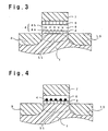
- An example of conventional MONOS memory is shown in Fig. 3.
- the shown MONOS memory has such a structure that a SiN x film 5, instead of the floating gate, is stacked upon a tunnel insulating film 2 as shown in Fig. 3.
- the MONOS memory is a memory which retains charges in interface levels 4a existing at the interfaces and in trap levels 4b discretely distributed in the SiN x film 5.
- reference numeral 1 designates a p-type single crystal Si substrate
- reference numeral 4 is a charge retention region
- reference numeral 6 designates a gate insulating film
- reference numeral 7 designates a control gate
- reference numeral 9 designates a source region
- reference numeral 10 designates a drain region
- reference numeral 11 designates a channel forming region.
- the interface levels 4a and the trap levels 4b which retain charges, are distributed in a spatially discrete manner, charge leakage only occurs locally even if dielectric breakdown is caused at a location in the tunnel insulating film. Hence, the charge retention ability of the memory cell does not change significantly before and after occurrence of the dielectric breakdown.
- MONOS memory is more excellent than the floating-gate-type flash memory in terms of the endurance and is regarded as being advantageous in terms of miniaturization or the like of the memory cells since the physical thickness of the tunnel insulating films can be made relatively thin.
- the depth of the trap levels of the SiN x film the energy difference between the trap level and the bottom of the conduction band for electrons, and the energy difference between the trap level and the top of the valence band for holes
- the absolute charge retention ability the charge retention ability of a device, which is in a normal state and is subjected to no dielectric breakdown
- a structure wherein floating gate is replaced by a plurality of nano-particles and the nano-particles are dispersed in the gate insulating film has been considered.
- FIG. 4 an example of semiconductor memory devices wherein nano-particles are formed from Si nano-particles is shown as a typical device having this structure.
- the same reference numerals as the elements in Fig. 3 indicate the same elements except for a charge retention region 4 in Fig. 4.
- a memory having this structure is disclosed in, e.g., JP-A-11-186421.
- This publication discloses a structure wherein a floating gate 4, which comprises a group of a plurality of Si nano-particle formed by a CVD method, is formed on a tunnel insulating film 2, and wherein the floating gate is covered with a gate insulating film 6.
- the currently available Si nano-particles have a size of from about 5 to about 10 nm and an in-plane distribution density (area density) of from 1 to 2 ⁇ 10 12 /cm 2 , and these values are insufficient in terms of memory function.
- the memory window (the shift width of threshold voltage in a MOS transistor) of the flash memory is narrowed since the area density of the amount of retained charges is also lowered.
- dispersion in the area density of the amount of charges among semiconductor memory cells are likely to be relatively large, which has an adverse influence on dispersion in the size of the memory window. Both phenomena make data reading operation unstable.
- the size of the floating gate 4 has to be reduced to have a diameter of about 1 nm.
- the smallest particle size of currently available nano-particles has remained at about 5 nm. Since it is necessary for at least one nano-particle to be formed in the gate region of a quite miniaturized single-electron memory with a high probability, it is required to have a high nano-particles formation density. From this viewpoint, the currently available area density of about 10 12 /cm 2 is insufficient. Further, in order to accomplish such area density, a quite peculiar pre-treatment is necessary which causes a problem of making the fabrication process complicate.
- the present invention provides a nonvolatile semiconductor memory device comprising a source region and a drain region formed on a surface of a semiconductor substrate; a tunnel insulating film formed in contact with a channel forming region so as to connect the source region and the drain region, the channel forming region being sandwiched between the source region and the drain region; a charge retention layer formed so as to be adjacent to the tunnel insulating film; a gate insulating film formed so as to be adjacent to the charge retention layer, and a control gate formed so as to be adjacent to the gate insulating film, characterized in that the charge retention layer is an insulating matrix containing, per one nonvolatile semiconductor memory cell, one nano-particle which is made of at least one type of single-element substance or at least one type of chemical compound that functions as a floating gate and has a particle size of at most 5 nm, or containing a plurality of such nano-particles independently dispersed with a density of from 10 +12 to 10 +14 particles per square centimeter of the charge
- the present invention also provides a nonvolatile semiconductor memory device comprising a source region and a drain region formed on a surface of a semiconductor substrate; a tunnel insulating film formed in contact with a channel forming region so as to connect the source region and the drain region, the channel forming region being sandwiched between the source region and the drain region; a charge retention layer formed so as to be adjacent to the tunnel insulating film; a floating gate formed so as to be adjacent to the charge retention layer, a gate insulating film formed so as to be adjacent to the floating gate, a gate insulating film formed so as to be adjacent to the floating gate, and a control gate formed so as to be adjacent to the gate insulating film, characterized in that the charge retention layer has a function to help electrons to transfer toward the floating gate from the channel forming region and to make it suppression that electron transfer toward the channel forming region from the floating gate.
- the present invention also provides the nonvolatile semiconductor memory device, wherein the charge retention layer is an insulating matrix containing a plurality of nano-particles which are made of at least one type of single-element substance or at least one type of chemical compound having a particle size of at most 5 nm, and which are independently dispersed with a density of from 10 +12 to 10 +14 particles per square centimeter.
- the charge retention layer is an insulating matrix containing a plurality of nano-particles which are made of at least one type of single-element substance or at least one type of chemical compound having a particle size of at most 5 nm, and which are independently dispersed with a density of from 10 +12 to 10 +14 particles per square centimeter.
- the present invention also provides the nonvolatile semiconductor memory device, wherein the nano-particles constituting the charge retention layer, are made of at least one type of single-element substance or at least one type of chemical compound selected from the group consisting of a metal, an oxide, a carbide, a nitride, a silicide and a boride.
- the present invention also provides the nonvolatile semiconductor memory device, wherein the insulating matrix constituting the charge retention layer is made of at least one type of chemical compound selected from the group consisting of an oxide, a carbide, a nitride, a boride, a silicide, and a fluoride.
- the present invention also provides the nonvolatile semiconductor memory device, wherein the nano-particles constituting the charge retention layer are dispersed two-dimensionally or three-dimensionally in the insulating matrix.
- the present invention also provides a process for producing the nonvolatile semiconductor memory device that has the charge retention layer wherein the nano-particles are dispersed two-dimensionally or three-dimensionally in the insulating matrix, characterized by forming the charge retention layer in a self-organizing manner by physical vapor deposition of each material to constitute the nano-particles and the insulating matrix.
- the present invention further provides the process for producing the nonvolatile semiconductor memory device of which the physical vapor deposition is performed by a sputtering method.
- a charge retention layer contains, per nonvolatile semiconductor memory cell, one nano-particle which is made of at least one type of single-element substance or at least one type of chemical compound that functions as a floating gate and has a particle size of at most 5 nm, or contains such nano-particles independently dispersed with a density of from 10 +12 to 10 +14 particles per square centimeter of the charge retention layer.
- a memory device containing one nano-particle per nonvolatile semiconductor memory cell, namely, per one memory cell may be utilized as a single-electron device.
- single-electron memory which provide one electron with one bit information, put one electron into a floating gate as an electron container or releases one electron from the floating gate.
- nano-particles are preferably formed with an area density of from about 10 13 to 10 14 /cm 2 .
- a technology for manufacturing single-electron memory device it is essential to develop a technology to form nano-particles with a quite high density, specifically, for example, with an area density of from 10 12 to 10 14 /cm 2 .
- FIG. 1 An embodiment of the nonvolatile semiconductor memory device according to the present invention is shown as a schematic cross-sectional view in Fig. 1.
- reference numeral 1 designates a p-type single crystal Si substrate
- reference numeral 2 designates a tunnel insulating film
- reference numeral 3 designates an charge retention layer, wherein nano-particles 3a as nano-particles are dispersively contained in an insulating matrix 3b.
- Reference numeral 6 designates a gate insulating matrix
- reference numeral 7 designates a control gate.
- Reference numeral 9 designates a source region
- reference numeral 10 designates a drain region
- reference numeral 11 designates an approximate region wherein a channel is formed, namely, a channel forming region.
- the p-type single crystal Si substrate 1 may comprise an SOI (Silicon On Insulator) substrate having a buried oxide film, which is suitably employed in a case wherein an attempt is made to realize an improvement in operation speed or a reduction in power consumption.
- the tunnel insulating film 2 may suitably comprise an oxide film, which has a relatively good boundary matching with the p-type single crystal Si substrate 1, or a material having a high dielectric constant in order to increase the controllability of an electric field distribution of the channel forming region 11 by control gate voltage, such as, a material of SiO x N y (0 ⁇ X ⁇ 2, 0 ⁇ y ⁇ 4/3).
- the film thickness of the tunnel insulating film be as thin as possible, in particular at most 8 nm. It is extremely preferable in terms of fast operation that the film thickness be at most 5 nm.
- the nano-particles 3a constituting the charge retention layer 3 are dispersed in a large number in order to suppress the loss amount of accumulated charges by dielectric breakdown of the tunnel insulating film 2 as low as possible, and it is preferred that the nano-particles be positioned at certain intervals so as to be electrically insulated from one another.
- the nano-particles in the charge retention layer have a high area density, in particular from 10 12 to 10 14 /cm 2 .
- the value of the area density conforms to the value of the area density referred to in explanation of single-electron memory devices, it is not necessarily meant that the number of the nano-particles is one per single-electron memory device in this case.
- the nano-particles are made to have a particle size of at most 5 nm. It is preferred to select a material having a high electron affinity (when the nano-particles are made of a semiconductor or insulating material) or a high work function (when the nano-particles are made of a good conductive material, such as metal) as the material of the nano-particles, or it is preferred to select a material having a low electron affinity as the material of the insulating matrix 3b.
- a high melting point material having resistance to high-temperature treatment in a semiconductor manufacturing process, for formation of the nano-particles and the insulating matrix 3b.
- a high melting point material having resistance to high-temperature treatment in a semiconductor manufacturing process, for formation of the nano-particles and the insulating matrix 3b.
- the specific names of materials suitable for the nano-particles and the insulating matrix will be described later.
- the physical thickness of the insulating film 6 is preferred, and it is preferred to select a material having a high dielectric constant for formation of the insulating film.
- the thickness is preferably at most 10 nm, and a SiO x N y material as stated earlier or laminated films of SiO 2 films and SiO x films in addition to a SiO 2 material may be suitably employed for the insulating film.
- a substrate 1 for forming a memory device comprises an SOI substrate, and the substrate 1 is constituted from three layers of a p-type single crystal Si substrate 1a, a buried oxide film 1b and a p-type SOI layer 1c.
- Reference numeral 2 designates a tunnel insulating film
- reference numeral 3 designates a charge retention layer, wherein nano-particles 3a are dispersively contained in an insulating matrix 3b.
- Reference numeral 4 designates a floating gate
- reference numeral 6 designates a gate insulating film
- reference numeral 7 designates a control gate
- reference numeral 8 designates a sidewall
- Reference numeral 9 designates a source region
- reference numeral 10 designates a drain region. In each of the regions, reference numerals 9a and 10a designate shallow junction regions, and reference numerals 9b and 10b designate contact regions.
- Reference numeral 11 designates an approximate region wherein a channel is formed, namely, a channel forming region.
- the tunnel insulating film 2 may be made of an oxide film, which has a good boundary matching with the p-type SOI layer 1c, or a material, which has a high dielectric constant in order to increase the controllability of an electric field distribution of the channel forming region 11 by control gate voltage, such as a SiO x N y material as stated earlier.
- control gate voltage such as a SiO x N y material as stated earlier.
- the film thickness of the tunnel insulating film 2 be as thin as possible, in particular at most 3 nm in consideration of the presence of the charge retention layer 3 stated later.
- the charge retention layer 3 has a function of helping electrons to transfer from the channel forming region 11 toward the floating gate 4 and of suppressing electrons to transfer from the floating gate 4 toward the channel forming region 11. The details will be explained below.
- the charge retention layer 3 is a layer which is disposed to suppress leakage of charges to the substrate, the charges having been accumulated in the floating gate 4 next to the charge retention layer 3.
- the charges are dispersively accumulated not only in the floating gate 4 but also in nano-particles 3a in the charge retention layer 3. Because the accumulated charges of nano-particles 3a have the Coulomb blockade effect on the accumulated charges in the floating gate 4, the leakage of the accumulated charges in the floating gate 4 toward the substrate is suppressed.
- the charge retention layer 3 is also effective in increase the writing speed.
- the writing operation may be performed even by application of a lower voltage. It is preferred that the nano-particles in the charge retention layer have a high charge retention ability. From the viewpoint of increasing the charge retention ability in the entire charge retention layer to eventually suppress the leakage of the charges retained in the floating gate 4, it is preferred that the nano-particles are dispersed with high density.
- the nano-particles have a three-dimensional multilayered structure with at least two layers of the nano-particles in order to increase the charge retention ability of the nano-particles.
- the respective nano-particles have a small size in order to exert the Coulomb blockage effect on the accumulated charges of the floating gate in a sufficient way.
- the area density of the nano-particles be as high as 10 12 to 10 14 /cm 2 .
- the size of the nano-particles is at most 5 nm, to use a material having a high electron affinity (in a case wherein the material of the nano-particles is a semiconductor or an electrically insulating material) or a large work function (in a case wherein the material of the nano-particles is a metal or the like) as the material of the nano-particles, and to select a material having a small electron affinity as the material of the insulating matrix 3b.
- a material having a high electron affinity in a case wherein the material of the nano-particles is a semiconductor or an electrically insulating material
- a large work function in a case wherein the material of the nano-particles is a metal or the like
- a high melting point material having resistance to high-temperature treatment in a semiconductor manufacturing, for formation of the nano-particles and the insulating matrix.
- the specific names of materials suitable for the nano-particles and the insulating matrix will be described later.
- a material having a high dielectric constant such as a SiO x N y material or laminated films of oxide films and SiN x films may be suitably employed for the insulating gate 6.
- a material having a high dielectric constant such as a SiO x N y material or laminated films of oxide films and SiN x films may be suitably employed for the insulating gate 6.
- the charge retention layer is formed by employing a physical vapor deposition method.
- a physical vapor deposition method As methods for forming a thin film, besides the physical vapor deposition method, for example, a chemical vapor deposition method (chemical vapor deposition method, also known as a CVD method) has been also well known.
- CVD method a single-phase film containing no separate phases, or a film having a high degree of crystallinity, that is to say, a film in an equilibrium phase is likely to be formed for, e.g., reasons that there is a high collision frequency between reactive atomic species and reactive molecular species in the vapor phase since the vapor phase pressure at film deposition is higher than physical film deposition, and that the vapor phase and the substrate surface has a high temperature.
- the chemical vapor deposition method is not suitable in a case wherein the nano-particles and the insulating matrix are separated as in the charge retention layer of the present invention, that is to say, wherein a film in a quasi-equilibrium phase or a nonequilibrium phase is formed.
- the charge retention layer may be formed with a one-step process by a physical vapor deposition method.
- physical vapor deposition method are a sputtering method, a thermal vapor deposition method, an electron beam vapor deposition method, a laser ablation method and a molecular beam epitaxy method.
- the sputtering method is particularly preferable for, e.g., reasons that it is possible to have a wide selection of film deposition materials, that it is easy to obtain a compact film and that it is possible to obtain a film having a good adhesive property with the foundation layer, and additionally that it is preferred for mass production.
- the sputtering method is preferable because it is possible to obtain a substrate temperature suitable for self-organization in the present invention.
- the self-organization can be promoted by causing particles of species for film deposition to appropriately migrate on a surface of the substrate, for example, because it is possible to obtain an appropriate substrate temperature, which is neither too high nor too low.
- one employing inductively coupled plasma or electromagnetic wave coupled plasma, or one employing a facing targets system is more preferable because of minimizing damage to the tunnel oxide film as the foundation layer.
- the charge retention layer is formed by the sputtering method
- a method to constitute a target by employing materials to form a dispersed phase as a nano-particle phase and materials to form a matrix phase as an insulating matrix phase there is no particular limitation to a method to constitute a target by employing materials to form a dispersed phase as a nano-particle phase and materials to form a matrix phase as an insulating matrix phase.
- One that is obtainable by sintering powder materials of both phases, or one that is obtainable by embedding an appropriate number of chip pieces of the materials of one of the phases in a single phase target of the material of the other phase so as to be exposed on a surface of the single phase target may be employed.
- a sputtering face of the target When a sputtering face of the target is set vertically upward in the film disposition chamber of a film deposition system, one that is obtainable by putting an appropriate number of chip pieces of the material of one of the phases on the single phase target of the material of the other phase, or one that is obtainable by only spreading mixed power of both phases in a glass petri dish or the like may be also employed as the target.
- a powder target is not preferable for producing a semiconductor chip, e.g., because there is a possibility that the powder can be scattered in a film depositing environment to have an adverse effect on another semiconductor manufacturing process.
- a combination of a material in a dispersed phase and a material in a matrix phase in a case of forming the charge retention layer a combination wherein the material of the dispersed phase and the material of the matrix phase undergo phase separation on film disposition, and wherein the work function or the electron affinity of the dispersed phase is greater than the electron affinity of the matrix phase is applicable.
- the self-organization of the present invention means that a group of atoms constituting for the nano-particles and a group of atoms constituting for the insulating matrix are separately disposed in a spontaneous manner by, e.g., the thermodynamic interaction, and that consequently, nano-particles are assembled on a nanoscale in the insulating matrix.
- This phenomenon depends on, e.g., a combination of the constituent material of the nano-particles and the constituent material of the insulating matrix, an existence ratio therebetween, and a film deposition condition, such as, a film deposition pressure or a substrate temperature.
- the action for self-organization can be relatively easily utilized to form the charge retention layer.
- the sputtering method it is possible to obtain a thermodynamic condition in a range appropriate for exhibiting the self-organization of the present invention.
- any one of a metal, a semiconductor and an insulator may be selected.
- a substance which has as large a work function and as large an electron affinity as possible for the purpose of having a better charge retention ability, and which has a high melting point for the purpose of being stabilized in heat treatment in the semiconductor manufacturing process.
- the nano-particles that are made of a metal may be made of an element, such as, Al, Ti, Zn, Ga, Zr, Nb, Mo, Re, Ru, In, Sn, La, Ta, Pt, W, Pb, Ag, Au or Pd, or a 3d transition metal element, such as, V, Cr, Mn, Ni, Fe, Co, or Cu, and/or an alloy containing one of them as a major component.
- an element such as, Al, Ti, Zn, Ga, Zr, Nb, Mo, Re, Ru, In, Sn, La, Ta, Pt, W, Pb, Ag, Au or Pd
- a 3d transition metal element such as, V, Cr, Mn, Ni, Fe, Co, or Cu, and/or an alloy containing one of them as a major component.
- the nano-particles which are made of an elemental semiconductor, are preferably made of at least one substance of Si, Ge, Se and Te.
- the nano-particles may contain at least one of elements, such as P, As, Sb, B, Al, Ga, In and Cu, as an impurity in at least one of semiconductors, such as, Si, Ge, Se and Te.
- the nano-particles that are made of a compound semiconductor or an insulator are preferably made of at least one of compound of InAs, InGaAs, InGaNAs, InAlAs, InAsP, InGaAsP, InSb, InGaSb, InAlSb, InGaAsSb, SiC, Cu 2 O, ZnO, CdO, BaO, PbO, NiO, In 2 O 3 , Sb 2 O 3 , SnO 2 , Ag 2 O, AgO, RuO 2 , V 3 Ga, Nb 3 Sn, Nb 3 Al, Nb 3 Ga, Nb 3 Ge, NbTi, NbMo 6 S 8 , ZnS, CdS, HgS, PbS, Sb 2 S 3 , Bi 2 S 3 , ZnSe, CdSe, HgSe, SnSe, PbSe, In 2 Se 3 , Sb 2 Se 3 , BiSe 3
- the nano-particles that are made of a compound semiconductor or an insulator may contain at least one of elements of Sn, Sb, Ga, Al and In, as an impurity in at least one selected from the substances group consisting of In 2 O 3 , Sb 2 O 3 , SnO 2 , ZnO and GaAs.
- An example of the material of the insulating matrix in the charge retention layer is at least one compound selected among an oxide, such as silica, alumina, titania, mullite, cordierite, spinel, zeolite or forsterite; carbide, such as boron carbide (B 4 C); nitride, such as silicon nitride, boron nitride or aluminum nitride; and fluoride, such as magnesium fluoride or aluminum fluoride. It is more preferable to select a substance, which has as low an electron affinity as possible for a better charge retention ability, and which has a high melting point for the purpose of being stabilized heat treatment in the semiconductor manufacturing process.
- an oxide such as silica, alumina, titania, mullite, cordierite, spinel, zeolite or forsterite
- carbide such as boron carbide (B 4 C)
- nitride such as silicon nitride, boron nitride or aluminum
- the average particle size of the dispersed phase growing in the matrix phase is changed by controlling the target composition and the film deposition condition. Particularly, it was observed that the average particle size changed according to the volume fraction of a target between the dispersed phase and the matrix phase and according to the film deposition condition (such as, an Ar gas pressure or a substrate temperature on sputtering).
- a target of Co-SiO 2 is employed to form a film having metal nano-particles of Co dispersed in a SiO 2 insulating matrix
- a target comprising Co and SiO 2 having a volume ratio of 50:50 it was observed that the particle size of the particles was about 2 nm for formation under an Ar gas pressure of 0.5 Pa while the size of the Co particles was about 5 nm for formation under an Ar gas pressure of 8 Pa.
- the charge retention layer of the nonvolatile semiconductor memory device wherein a material having a large work function or a large electron affinity comprises nano-particles having a particle size of at most 5 nm, and wherein a thin film having the nano-particles dispersed with a high density in the insulating matrix is employed, can independently retain a large number of charges in a dispersed manner.
- the charge retention layer of the nonvolatile semiconductor memory device according to the present invention wherein a material having a large work function or a large electron affinity comprises nano-particles having a particle size of at most 5 nm, and wherein a thin film having the nano-particles dispersed with a high density in the insulating matrix is employed, can reduce the electric capacities which are formed between individual nano-particles, between the nano-particles and the semiconductor substrate, and between the nano-particles and the floating gate.
- composition materials can be selected for the dispersed phase and the matrix phase. Since it is easily possible to incorporate the sputtering method into a conventional semiconductor manufacturing process as a film deposition process, it is possible to provide a high performance nonvolatile semiconductor memory device with good reproducibility and without major modifications in the conventional process.
- a tunnel insulating film 2 was formed on a p-type single-crystal Si substrate 1.
- the tunnel insulating film 2 was prepared by subjecting a semiconductor substrate to thermal oxidation at 800°C and had a thickness of 3 nm.
- a charge retention layer 3 which was constituted from an insulating matrix 3b containing nano-particles 3a for charge retention, was formed so as to have a thickness of 7 nm by a capacitively coupled type magnetron sputtering method as described below.
- Metal Co and SiO 2 were selected for the nano-particles and the insulating matrix, respectively.
- a composite target which comprised a metal Co target having a diameter of 6 inches (15.24 cm) and SiO 2 glass chips having 5 mm square and placed thereon was employed. The amount of the SiO 2 glass chip was adjusted to occupy 70% of the area of the surface that was exposed to plasma of the target.
- a phosphorus doped polysilicon layer as the control gate 7 was formed by CVD.
- a photoresist layer was formed as a mask. Portions of the control gate 7 of the polysilicon, the gate insulating film 6, the charge retention layer 3 and the tunnel insulating film 2, which were not covered with the mask, were removed by a dry etching method to form a gate structure. And then, a source region 9 and a drain region 10 were formed by arsenic ion implantation (arsenic may be replaced by phosphorus) and by annealing.
- the nonvolatile semiconductor memory device in this example will be explained, referring to Fig. 2.
- the SOI substrate comprised a p-type single-crystal Si substrate 1a, a buried oxide film 1b and a p-type SOI layer 1c.
- An oxide film as a tunnel insulating film 2 was formed on the p-type SOI layer 1c so as to have a thickness of 1.5 nm by thermal oxidation at 800°C.
- a charge retention layer 3 which comprised an insulating matrix 3b three-dimensionally containing nano-particles 3a was formed so as to have a thickness of 10 nm by a sputtering method in the manner described below.
- a thin film comprising two-phases of Pt and SiO 2 was formed.
- a composite target with a diameter of 6 inches (15.24 cm) which was prepared by mixing Pt powder and SiO 2 powder with a volume proportion of 20:80 and then sintering the mixture was employed.
- a film of Si poly crystal as a floating gate 4 was deposited by CVD, a SiO 2 film was further deposited on the Si film by CVD, and then a SiN x layer was formed as a gate insulating film 6 by thermal nitriding.
- a phosphorus doped polysilicon layer as a control gate 7 by CVD
- the control gate 7, the gate insulating film 6, the floating gate 4, the charge retention layer 3 and the tunnel insulating film 2 were partially removed by a dry etching method to form a gate structure.
- phosphorus ion implantation (phosphorus may be replaced by arsenic) was performed with shallow penetration by low energy to form shallow junction regions 9a and 10a.
- the gate structure which specifically comprised the tunnel insulating film 2, the charge retention layer 3, the floating gate 4, the gate insulating film 6 and the control gate 7 was once entirely covered by a SiO 2 film deposited by CVD.
- a side-wall 8 was formed by partially etching (etching back) the SiO 2 film by a dry etching method.
- phosphorus ion implantation (phosphorus may be replaced by arsenic) was performed with slightly deeper penetration by high energy to form contact regions 9b and 10b.
- a source region 9 and a drain region 10 were formed by annealing.
- the nonvolatile semiconductor memory device can shorten data writing and erasing time, significantly improve the endurance characteristic and be operated with low power consumption in comparison with conventional similar memory devices.
- the nonvolatile semiconductor device according to the present invention can be applied to equipment and a technical field that conventional nonvolatile semiconductor devices have not been applied to. It is supposed that the nonvolatile semiconductor device according to the present invention can be widely applied to mobile information devices, can make PC-carried memories non-volatilization due to replacement from DRAM and can be also applied to single-electron device that is said to be ultimate memory device.
- a sputtering method it is possible to widely select materials comprising various compositions as the material to form nano-particles and to relatively freely control the particle size of the nano-particles by changing a deposition condition.
- suitable materials for a purpose.
- a magnetic metal or a magnetic semiconductor as the material of the nano-particles
- a sputtering method it is possible to easily incorporate the method according to the present invention into a conventional semiconductor production process. Further, it is possible to form an artificial lattice by laminating various sorts of materials alternately.
Landscapes
- Engineering & Computer Science (AREA)
- Chemical & Material Sciences (AREA)
- Nanotechnology (AREA)
- Physics & Mathematics (AREA)
- Mathematical Physics (AREA)
- Theoretical Computer Science (AREA)
- Crystallography & Structural Chemistry (AREA)
- Non-Volatile Memory (AREA)
- Semiconductor Memories (AREA)
- Physical Vapour Deposition (AREA)
Abstract
Description
Although the value of the area density conforms to the value of the area density referred to in explanation of single-electron memory devices, it is not necessarily meant that the number of the nano-particles is one per single-electron memory device in this case.
Claims (8)
- A nonvolatile semiconductor memory device comprising a source region and a drain region formed on a surface of a semiconductor substrate; a tunnel insulating film formed in contact with a channel forming region so as to connect the source region and the drain region, the channel forming region being sandwiched between the source region and the drain region; a charge retention layer formed adjacent the tunnel insulating film; a gate insulating film formed adjacent the charge retention layer, and a control gate formed adjacent the gate insulating film, characterized in that the charge retention layer is an insulating matrix containing, per nonvolatile semiconductor memory cell, one nano-particle which is made of at least one type of single-element substance or at least one type of chemical compound that functions as a floating gate and has a particle size of at most 5 nm, or containing a plurality of such nano-particles independently dispersed with a density of from 1012 to 1014 particles per square centimeter of the charge retention layer.
- A nonvolatile semiconductor memory device comprising a source region and a drain region formed on a surface of a semiconductor substrate; a tunnel insulating film formed in contact with a channel forming region so as to connect the source region and the drain region, the channel forming region being sandwiched between the source region and the drain region; a charge retention layer formed adjacent the tunnel insulating film; a floating gate formed adjacent the charge retention layer, a gate insulating film formed adjacent the floating gate, and a control gate formed adjacent the gate insulating film, characterized in that the charge retention layer has a function to help electrons to transfer from the channel forming region toward the floating gate and to suppress electron transfer toward the channel forming region from the floating gate.
- The nonvolatile semiconductor memory device according to Claim 2, wherein the charge retention layer is an insulating matrix containing a plurality of nano-particles which are made of at least one type of single-element substance or at least one type of chemical compound having a particle size of at most 5 nm and are independently dispersed with a density of from 1012 to 1014 particles per square centimeter.
- The nonvolatile semiconductor memory device according to Claim 1, 2 or 3, wherein the nano-particles constituting the charge retention layer, are made of at least one type of single-element substance or at least one type of chemical compound selected from the group consisting of a metal, an oxide, a carbide, a nitride, a silicide and a boride.
- The nonvolatile semiconductor memory device according to Claim 1, 2 or 3, wherein the insulating matrix constituting the charge retention layer is made of at least one type of chemical compound selected from the group consisting of an oxide, a carbide, a nitride, a boride, a silicide, and a fluoride.
- The nonvolatile semiconductor memory device according to Claim 1, 2 or 3, wherein the nano-particles constituting the charge retention layer are dispersed two-dimensionally or three-dimensionally in the insulating matrix.
- A process for producing the nonvolatile semiconductor memory device that has the charge retention layer wherein the nano-particles are dispersed two-dimensionally or three-dimensionally in the insulating matrix as defined in Claim 6, characterized by forming the charge retention layer in a self-organizing manner by physical vapor deposition of each material to constitute the nano-particles and the insulating matrix.
- The process for producing the nonvolatile semiconductor memory device according to Claim 7, wherein the physical vapor deposition is performed by a sputtering method.
Applications Claiming Priority (3)
| Application Number | Priority Date | Filing Date | Title |
|---|---|---|---|
| JP2002213900 | 2002-07-23 | ||
| JP2002213900A JP4056817B2 (en) | 2002-07-23 | 2002-07-23 | Method for manufacturing nonvolatile semiconductor memory element |
| PCT/JP2003/009335 WO2004010508A1 (en) | 2002-07-23 | 2003-07-23 | Nonvolatile semiconductor storage device and manufacturing method |
Publications (2)
| Publication Number | Publication Date |
|---|---|
| EP1536483A1 true EP1536483A1 (en) | 2005-06-01 |
| EP1536483A4 EP1536483A4 (en) | 2008-07-16 |
Family
ID=30767855
Family Applications (1)
| Application Number | Title | Priority Date | Filing Date |
|---|---|---|---|
| EP03765365A Withdrawn EP1536483A4 (en) | 2002-07-23 | 2003-07-23 | NON-VOLATILE SEMICONDUCTOR MEMORY AND METHOD FOR MANUFACTURING THE SAME |
Country Status (7)
| Country | Link |
|---|---|
| US (1) | US7550802B2 (en) |
| EP (1) | EP1536483A4 (en) |
| JP (1) | JP4056817B2 (en) |
| KR (1) | KR100958556B1 (en) |
| AU (1) | AU2003252675A1 (en) |
| TW (1) | TW200402849A (en) |
| WO (1) | WO2004010508A1 (en) |
Cited By (4)
| Publication number | Priority date | Publication date | Assignee | Title |
|---|---|---|---|---|
| EP1737033A4 (en) * | 2004-04-16 | 2007-10-24 | Asahi Glass Co Ltd | NON-VOLATILE SEMICONDUCTOR STORAGE ELEMENT HAVING HIGH LOAD PRESERVATION CHARACTERISTICS AND METHOD OF MANUFACTURING THE SAME |
| EP1689002A3 (en) * | 2005-02-03 | 2009-04-22 | Samsung Electronics Co., Ltd. | Nonvolatile memory device and method of manufacturing the same |
| CN100595907C (en) * | 2005-09-12 | 2010-03-24 | 旭硝子株式会社 | Nonvolatile semiconductor memory element having good charge retention characteristics and method of manufacturing the same |
| WO2020100051A1 (en) * | 2018-11-13 | 2020-05-22 | Khalifa University of Science and Technology | Non-volatile memory systems based on single nanoparticles for compact and high data storage electronic devices |
Families Citing this family (78)
| Publication number | Priority date | Publication date | Assignee | Title |
|---|---|---|---|---|
| US7121474B2 (en) * | 2002-06-18 | 2006-10-17 | Intel Corporation | Electro-optical nanocrystal memory device |
| JP4056817B2 (en) | 2002-07-23 | 2008-03-05 | 光正 小柳 | Method for manufacturing nonvolatile semiconductor memory element |
| WO2004019294A2 (en) * | 2002-08-23 | 2004-03-04 | General Electric Company | Rapidly responding, false detection immune alarm signal producing smoke detector |
| KR100446632B1 (en) * | 2002-10-14 | 2004-09-04 | 삼성전자주식회사 | Nonvolatile Silicon/Oxide/Nitride/Silicon/ Nitride/Oxide/ Silicon memory |
| JP2006516819A (en) * | 2003-01-30 | 2006-07-06 | ユニバーシティ・オブ・ケープ・タウン | Thin film semiconductor device and manufacturing method of thin film semiconductor device |
| US7083586B2 (en) * | 2003-02-03 | 2006-08-01 | Dj Orthopedics, Llc | Patellofemoral brace |
| US20050095786A1 (en) * | 2003-11-03 | 2005-05-05 | Ting-Chang Chang | Non-volatile memory and method of manufacturing floating gate |
| TWI276206B (en) * | 2003-11-25 | 2007-03-11 | Promos Technologies Inc | Method for fabricating flash memory device and structure thereof |
| US7595528B2 (en) * | 2004-03-10 | 2009-09-29 | Nanosys, Inc. | Nano-enabled memory devices and anisotropic charge carrying arrays |
| US7968273B2 (en) | 2004-06-08 | 2011-06-28 | Nanosys, Inc. | Methods and devices for forming nanostructure monolayers and devices including such monolayers |
| US8563133B2 (en) * | 2004-06-08 | 2013-10-22 | Sandisk Corporation | Compositions and methods for modulation of nanostructure energy levels |
| TWI406890B (en) * | 2004-06-08 | 2013-09-01 | Sandisk Corp | Post-deposition encapsulation of nanostructures : compositions, devices and systems incorporating same |
| US7776758B2 (en) | 2004-06-08 | 2010-08-17 | Nanosys, Inc. | Methods and devices for forming nanostructure monolayers and devices including such monolayers |
| US8088483B1 (en) | 2004-06-08 | 2012-01-03 | Nanosys, Inc. | Process for group 10 metal nanostructure synthesis and compositions made using same |
| US7501315B2 (en) * | 2004-06-08 | 2009-03-10 | Nanosys, Inc. | Methods and devices for forming nanostructure monolayers and devices including such monolayers |
| US7208793B2 (en) * | 2004-11-23 | 2007-04-24 | Micron Technology, Inc. | Scalable integrated logic and non-volatile memory |
| CN100508167C (en) | 2004-11-30 | 2009-07-01 | 富士通微电子株式会社 | Semiconductor memory device and method of manufacturing the same |
| US7355238B2 (en) * | 2004-12-06 | 2008-04-08 | Asahi Glass Company, Limited | Nonvolatile semiconductor memory device having nanoparticles for charge retention |
| JP5481468B2 (en) * | 2004-12-10 | 2014-04-23 | 株式会社東芝 | Semiconductor device |
| JP4744885B2 (en) * | 2005-01-18 | 2011-08-10 | 株式会社東芝 | Manufacturing method of semiconductor device |
| KR20060095819A (en) * | 2005-02-28 | 2006-09-04 | 삼성전자주식회사 | Method for manufacturing memory device using metal nitride as trap site |
| US7575693B2 (en) * | 2005-05-23 | 2009-08-18 | Nantero, Inc. | Method of aligning nanotubes and wires with an etched feature |
| US7541216B2 (en) * | 2005-06-09 | 2009-06-02 | Nantero, Inc. | Method of aligning deposited nanotubes onto an etched feature using a spacer |
| US7956608B1 (en) * | 2005-06-27 | 2011-06-07 | Northwestern University | Method of using group III-V ferromagnetic/non-magnetic semiconductor heterojunctions and magnetodiodes |
| KR100683854B1 (en) * | 2005-09-06 | 2007-02-15 | 삼성전자주식회사 | Methods of forming non-volatile memory device |
| JP4876520B2 (en) * | 2005-10-07 | 2012-02-15 | ソニー株式会社 | Nonvolatile semiconductor memory and manufacturing method thereof |
| JP2007227694A (en) * | 2006-02-24 | 2007-09-06 | Sanyo Electric Co Ltd | Semiconductor device and manufacturing method thereof |
| US20070221983A1 (en) * | 2006-03-24 | 2007-09-27 | Bohumil Lojek | Dual gate memory with fast erase |
| US7786526B2 (en) | 2006-03-31 | 2010-08-31 | Semiconductor Energy Laboratory Co., Ltd. | Nonvolatile semiconductor memory device |
| KR100740613B1 (en) * | 2006-07-03 | 2007-07-18 | 삼성전자주식회사 | Method of forming nonvolatile memory device |
| US7667260B2 (en) * | 2006-08-09 | 2010-02-23 | Micron Technology, Inc. | Nanoscale floating gate and methods of formation |
| JP4282702B2 (en) | 2006-09-22 | 2009-06-24 | 株式会社東芝 | Nonvolatile semiconductor memory device |
| KR100851553B1 (en) | 2006-10-02 | 2008-08-11 | 삼성전자주식회사 | Image sensor and method of driving the same |
| US20080128786A1 (en) * | 2006-12-04 | 2008-06-05 | Electronics And Telecommunications Research Institute | High density semiconductor memory device and method for manufacturing the same |
| KR100779566B1 (en) * | 2006-12-08 | 2007-11-28 | 한양대학교 산학협력단 | Nano floating gate type nonvolatile semiconductor memory device and manufacturing method thereof |
| JP4594971B2 (en) * | 2007-01-19 | 2010-12-08 | 国立大学法人広島大学 | Semiconductor memory, semiconductor memory system using the same, and method of manufacturing quantum dots used in semiconductor memory |
| KR101341571B1 (en) | 2007-04-30 | 2013-12-16 | 삼성전자주식회사 | Non-volatile memory device and method of manufacturing the same |
| JP2008288346A (en) * | 2007-05-16 | 2008-11-27 | Hiroshima Univ | Semiconductor element |
| JP2009018403A (en) * | 2007-07-13 | 2009-01-29 | Toyota Central R&D Labs Inc | Precious metal nanoparticle-dispersed thin film and method for producing the same |
| JP2009081203A (en) | 2007-09-25 | 2009-04-16 | Toshiba Corp | Nonvolatile semiconductor memory device and manufacturing method thereof |
| US8193055B1 (en) | 2007-12-18 | 2012-06-05 | Sandisk Technologies Inc. | Method of forming memory with floating gates including self-aligned metal nanodots using a polymer solution |
| US7723186B2 (en) * | 2007-12-18 | 2010-05-25 | Sandisk Corporation | Method of forming memory with floating gates including self-aligned metal nanodots using a coupling layer |
| JP2009231373A (en) * | 2008-03-19 | 2009-10-08 | Toshiba Corp | Nonvolatile semiconductor memory device |
| JP5295606B2 (en) | 2008-03-28 | 2013-09-18 | 株式会社東芝 | NAND type nonvolatile semiconductor memory device |
| JP2010050168A (en) * | 2008-08-19 | 2010-03-04 | Ulvac Japan Ltd | Method of fabricating nanodot, and floating gate transistor, and method of fabricating the same |
| JP5355980B2 (en) * | 2008-09-29 | 2013-11-27 | 株式会社東芝 | Nonvolatile semiconductor memory device and driving method thereof |
| US7897954B2 (en) | 2008-10-10 | 2011-03-01 | Macronix International Co., Ltd. | Dielectric-sandwiched pillar memory device |
| US7829445B2 (en) | 2008-10-24 | 2010-11-09 | Samsung Electronics Co., Ltd. | Method of manufacturing a flash memory device |
| US8891283B2 (en) * | 2009-01-05 | 2014-11-18 | Hewlett-Packard Development Company, L.P. | Memristive device based on current modulation by trapped charges |
| US8093129B2 (en) * | 2009-02-03 | 2012-01-10 | Micron Technology, Inc. | Methods of forming memory cells |
| JP4368934B1 (en) | 2009-02-09 | 2009-11-18 | アイランド ジャイアント デベロップメント エルエルピー | Liquid storage system, liquid storage container, and liquid derivation control method |
| JP5531252B2 (en) * | 2009-03-04 | 2014-06-25 | 株式会社東芝 | Nonvolatile semiconductor memory |
| US8383479B2 (en) | 2009-07-21 | 2013-02-26 | Sandisk Technologies Inc. | Integrated nanostructure-based non-volatile memory fabrication |
| JP5637712B2 (en) * | 2010-03-26 | 2014-12-10 | 公益財団法人電磁材料研究所 | Semiconductor nanocomposite structure thin film material and manufacturing method thereof |
| US8575678B2 (en) | 2011-01-13 | 2013-11-05 | Semiconductor Energy Laboratory Co., Ltd. | Semiconductor memory device with floating gate |
| US8329543B2 (en) | 2011-04-12 | 2012-12-11 | Freescale Semiconductor, Inc. | Method for forming a semiconductor device having nanocrystals |
| US8329544B2 (en) | 2011-04-12 | 2012-12-11 | Freescale Semiconductor, Inc. | Method for forming a semiconductor device having nanocrystals |
| KR101515874B1 (en) | 2011-06-24 | 2015-05-04 | 휴렛-팩커드 디벨롭먼트 컴퍼니, 엘.피. | High-reliability high-speed memristor |
| US9001564B2 (en) | 2011-06-29 | 2015-04-07 | Semiconductor Energy Laboratory Co., Ltd. | Semiconductor device and a method for driving the same |
| KR20130037063A (en) * | 2011-10-05 | 2013-04-15 | 에스케이하이닉스 주식회사 | 3d structured nonvolatile memory device and method for manufacturing the same |
| US8679912B2 (en) | 2012-01-31 | 2014-03-25 | Freescale Semiconductor, Inc. | Semiconductor device having different non-volatile memories having nanocrystals of differing densities and method therefor |
| JP5878797B2 (en) * | 2012-03-13 | 2016-03-08 | ルネサスエレクトロニクス株式会社 | Semiconductor device and manufacturing method thereof |
| JP2013197269A (en) | 2012-03-19 | 2013-09-30 | Toshiba Corp | Nonvolatile semiconductor storage device |
| US8822288B2 (en) | 2012-07-02 | 2014-09-02 | Sandisk Technologies Inc. | NAND memory device containing nanodots and method of making thereof |
| US8994006B2 (en) | 2012-10-02 | 2015-03-31 | International Business Machines Corporation | Non-volatile memory device employing semiconductor nanoparticles |
| US8823075B2 (en) | 2012-11-30 | 2014-09-02 | Sandisk Technologies Inc. | Select gate formation for nanodot flat cell |
| US8987802B2 (en) | 2013-02-28 | 2015-03-24 | Sandisk Technologies Inc. | Method for using nanoparticles to make uniform discrete floating gate layer |
| US9331181B2 (en) * | 2013-03-11 | 2016-05-03 | Sandisk Technologies Inc. | Nanodot enhanced hybrid floating gate for non-volatile memory devices |
| US9385239B2 (en) | 2013-03-15 | 2016-07-05 | Applied Materials, Inc. | Buffer layers for metal oxide semiconductors for TFT |
| US9177808B2 (en) | 2013-05-21 | 2015-11-03 | Sandisk Technologies Inc. | Memory device with control gate oxygen diffusion control and method of making thereof |
| US8969153B2 (en) | 2013-07-01 | 2015-03-03 | Sandisk Technologies Inc. | NAND string containing self-aligned control gate sidewall cladding |
| CN103824888A (en) * | 2014-02-28 | 2014-05-28 | 苏州大学 | Semiconductor device with micro-floating structure |
| US9735359B2 (en) * | 2014-04-23 | 2017-08-15 | Micron Technology, Inc. | Methods of forming a memory cell material, and related methods of forming a semiconductor device structure, memory cell materials, and semiconductor device structures |
| US9466731B2 (en) * | 2014-08-12 | 2016-10-11 | Empire Technology Development Llc | Dual channel memory |
| CN109576659A (en) * | 2019-01-10 | 2019-04-05 | 广东省测试分析研究所(中国广州分析测试中心) | The magnetron sputtering preparation method of gradient auto-dope pure phase multi-element metal oxide film |
| CN111834393B (en) * | 2019-04-22 | 2022-12-02 | 辽宁冷芯半导体科技有限公司 | Flexible carbon nanotube photoelectric memory based on aluminum nanocrystalline floating gate |
| CN112908999A (en) * | 2021-03-25 | 2021-06-04 | 复旦大学 | Manufacturing process of semi-floating gate memory and semi-floating gate memory |
| CN112909000B (en) * | 2021-03-25 | 2022-10-21 | 复旦大学 | Semi-floating gate memory and its manufacturing process |
Family Cites Families (23)
| Publication number | Priority date | Publication date | Assignee | Title |
|---|---|---|---|---|
| US3878549A (en) * | 1970-10-27 | 1975-04-15 | Shumpei Yamazaki | Semiconductor memories |
| US4949136A (en) * | 1988-06-09 | 1990-08-14 | University Of Connecticut | Submicron lightly doped field effect transistors |
| JPH0936317A (en) * | 1995-07-17 | 1997-02-07 | Matsushita Electric Ind Co Ltd | Memory device and manufacturing method thereof |
| JP3512975B2 (en) * | 1997-03-14 | 2004-03-31 | 株式会社東芝 | Semiconductor device and manufacturing method thereof |
| JPH1187544A (en) * | 1997-09-12 | 1999-03-30 | Hiroshima Univ | Semiconductor storage device using quantum structure |
| US6670188B1 (en) | 1998-04-24 | 2003-12-30 | Crucell Holland B.V. | Packaging systems for human recombinant adenovirus to be used in gene therapy |
| JP2000022092A (en) * | 1998-07-03 | 2000-01-21 | Nippon Telegr & Teleph Corp <Ntt> | Single electron memory element |
| JP3824787B2 (en) * | 1998-09-07 | 2006-09-20 | 独立行政法人科学技術振興機構 | Manufacturing method and manufacturing apparatus of ultrafine particle dispersion film |
| US6548825B1 (en) * | 1999-06-04 | 2003-04-15 | Matsushita Electric Industrial Co., Ltd. | Semiconductor device including barrier layer having dispersed particles |
| JP2001313342A (en) | 1999-06-04 | 2001-11-09 | Matsushita Electric Ind Co Ltd | Semiconductor device and method of manufacturing the same |
| US6984842B1 (en) * | 1999-10-25 | 2006-01-10 | The Board Of Trustees Of The University Of Illinois | Silicon nanoparticle field effect transistor and transistor memory device |
| EP1252658A4 (en) * | 2000-02-02 | 2008-02-13 | Univ Illinois | SILICON NANOTEILIC FIELD EFFECT TRANSISTOR AND TRANSISTOR MEMORY ELEMENT |
| US6413819B1 (en) * | 2000-06-16 | 2002-07-02 | Motorola, Inc. | Memory device and method for using prefabricated isolated storage elements |
| US6297095B1 (en) * | 2000-06-16 | 2001-10-02 | Motorola, Inc. | Memory device that includes passivated nanoclusters and method for manufacture |
| JP2002100687A (en) * | 2000-09-21 | 2002-04-05 | Toshiba Corp | Semiconductor storage element |
| US6646302B2 (en) * | 2000-11-21 | 2003-11-11 | Cornell Research Foundation, Inc. | Embedded metal nanocrystals |
| US6444545B1 (en) * | 2000-12-19 | 2002-09-03 | Motorola, Inc. | Device structure for storing charge and method therefore |
| JP2002222880A (en) | 2001-01-29 | 2002-08-09 | Asahi Glass Co Ltd | Coating solution for forming charge retention layer and nonvolatile semiconductor memory device |
| US6918946B2 (en) * | 2001-07-02 | 2005-07-19 | Board Of Regents, The University Of Texas System | Applications of light-emitting nanoparticles |
| US6656792B2 (en) * | 2001-10-19 | 2003-12-02 | Chartered Semiconductor Manufacturing Ltd | Nanocrystal flash memory device and manufacturing method therefor |
| US6784480B2 (en) * | 2002-02-12 | 2004-08-31 | Micron Technology, Inc. | Asymmetric band-gap engineered nonvolatile memory device |
| US7005697B2 (en) * | 2002-06-21 | 2006-02-28 | Micron Technology, Inc. | Method of forming a non-volatile electron storage memory and the resulting device |
| JP4056817B2 (en) | 2002-07-23 | 2008-03-05 | 光正 小柳 | Method for manufacturing nonvolatile semiconductor memory element |
-
2002
- 2002-07-23 JP JP2002213900A patent/JP4056817B2/en not_active Expired - Fee Related
-
2003
- 2003-07-22 TW TW092120003A patent/TW200402849A/en not_active IP Right Cessation
- 2003-07-23 EP EP03765365A patent/EP1536483A4/en not_active Withdrawn
- 2003-07-23 WO PCT/JP2003/009335 patent/WO2004010508A1/en not_active Ceased
- 2003-07-23 AU AU2003252675A patent/AU2003252675A1/en not_active Abandoned
- 2003-07-23 KR KR1020057000573A patent/KR100958556B1/en not_active Expired - Fee Related
-
2005
- 2005-01-12 US US11/033,142 patent/US7550802B2/en not_active Expired - Fee Related
Cited By (9)
| Publication number | Priority date | Publication date | Assignee | Title |
|---|---|---|---|---|
| EP1737033A4 (en) * | 2004-04-16 | 2007-10-24 | Asahi Glass Co Ltd | NON-VOLATILE SEMICONDUCTOR STORAGE ELEMENT HAVING HIGH LOAD PRESERVATION CHARACTERISTICS AND METHOD OF MANUFACTURING THE SAME |
| EP1689002A3 (en) * | 2005-02-03 | 2009-04-22 | Samsung Electronics Co., Ltd. | Nonvolatile memory device and method of manufacturing the same |
| US7785996B2 (en) | 2005-02-03 | 2010-08-31 | Samsung Electronics Co., Ltd. | Nonvolatile memory device and method of manufacturing the same |
| CN100595907C (en) * | 2005-09-12 | 2010-03-24 | 旭硝子株式会社 | Nonvolatile semiconductor memory element having good charge retention characteristics and method of manufacturing the same |
| US7820515B2 (en) | 2005-09-12 | 2010-10-26 | Asahi Glass Company, Limited | Nonvolatile semiconductor memory element excellent in charge retention properties and process for producing the same |
| EP1933378A4 (en) * | 2005-09-12 | 2014-08-13 | Asahi Glass Co Ltd | NON-VOLATILE SEMICONDUCTOR MEMORY ELEMENT HAVING EXCELLENT CHARGE RETENTION PROPERTIES AND METHOD FOR PRODUCING THE SAME |
| WO2020100051A1 (en) * | 2018-11-13 | 2020-05-22 | Khalifa University of Science and Technology | Non-volatile memory systems based on single nanoparticles for compact and high data storage electronic devices |
| EP3880602A4 (en) * | 2018-11-13 | 2021-12-15 | Khalifa University of Science and Technology | NON-VOLATILE STORAGE SYSTEMS BASED ON INDIVIDUAL NANOPARTICLES FOR COMPACT ELECTRONIC DEVICES WITH HIGH DATA STORAGE |
| US12249638B2 (en) | 2018-11-13 | 2025-03-11 | Khalifa University of Science and Technology | Non-volatile memory systems based on single nanoparticles for compact and high data storage electronic devices |
Also Published As
| Publication number | Publication date |
|---|---|
| US7550802B2 (en) | 2009-06-23 |
| TWI319219B (en) | 2010-01-01 |
| TW200402849A (en) | 2004-02-16 |
| US20050122775A1 (en) | 2005-06-09 |
| KR100958556B1 (en) | 2010-05-18 |
| WO2004010508A1 (en) | 2004-01-29 |
| KR20050025350A (en) | 2005-03-14 |
| EP1536483A4 (en) | 2008-07-16 |
| JP2004055969A (en) | 2004-02-19 |
| JP4056817B2 (en) | 2008-03-05 |
| AU2003252675A1 (en) | 2004-02-09 |
Similar Documents
| Publication | Publication Date | Title |
|---|---|---|
| US7550802B2 (en) | Nonvolatile semiconductor memory device and manufacturing process of the same | |
| US7355238B2 (en) | Nonvolatile semiconductor memory device having nanoparticles for charge retention | |
| JP2004055969A5 (en) | ||
| US10727249B2 (en) | Memory cells, integrated structures and memory arrays | |
| US6444545B1 (en) | Device structure for storing charge and method therefore | |
| CN101589461B (en) | Electron blocking layers for electronic devices | |
| KR100996191B1 (en) | Nonvolatile Memory Device and Manufacturing Method Thereof | |
| US20060124991A1 (en) | Semiconductor device | |
| JP2010531048A (en) | Electronic block layer for electronic devices | |
| US12058871B2 (en) | Semiconductor device including ferroelectric layer and metal particles embedded in metal-organic framework layer | |
| JP2001313342A (en) | Semiconductor device and method of manufacturing the same | |
| JP4253473B2 (en) | Semiconductor device and manufacturing method thereof | |
| EP1737033A1 (en) | Nonvolatile semiconductor storage element having high charge holding characteristics and method for fabricating the same | |
| US20080150004A1 (en) | Electron Blocking Layers for Electronic Devices | |
| US8481386B2 (en) | Nanocrystal memories and methods of forming the same | |
| JP5306604B2 (en) | Binary semiconductor memory device | |
| JP2005328029A (en) | Nonvolatile semiconductor memory device and manufacturing method thereof | |
| JP2005340768A (en) | Multi-value nonvolatile semiconductor memory element and manufacturing method thereof | |
| US20070190721A1 (en) | Semiconductor memory device having an alloy metal gate electrode and method of manufacturing the same | |
| US20100044775A1 (en) | Semiconductor memory device and semiconductor device | |
| KR100652135B1 (en) | Organic Nonvolatile Memory Device Having a Stable Multi-Layer Quantum Dot and Manufacturing Method Thereof | |
| JP2013077603A (en) | Memory device | |
| KR20070022682A (en) | Nonvolatile semiconductor memory device and manufacturing method having high charge retention characteristics | |
| KR100652134B1 (en) | Nonvolatile Memory Device and Manufacturing Method Thereof | |
| JP2003347440A (en) | Semiconductor element |
Legal Events
| Date | Code | Title | Description |
|---|---|---|---|
| PUAI | Public reference made under article 153(3) epc to a published international application that has entered the european phase |
Free format text: ORIGINAL CODE: 0009012 |
|
| 17P | Request for examination filed |
Effective date: 20050113 |
|
| AK | Designated contracting states |
Kind code of ref document: A1 Designated state(s): AT BE BG CH CY CZ DE DK EE ES FI FR GB GR HU IE IT LI LU MC NL PT RO SE SI SK TR |
|
| AX | Request for extension of the european patent |
Extension state: AL LT LV MK |
|
| DAX | Request for extension of the european patent (deleted) | ||
| RBV | Designated contracting states (corrected) |
Designated state(s): DE FR GB IT |
|
| RIN1 | Information on inventor provided before grant (corrected) |
Inventor name: KONDOH, SHINJI,C/O ASAHI GLASS COMPANY, LTD Inventor name: TAKATA, MASAAKI Inventor name: KOYANAGI, MITSUMASA |
|
| RIN1 | Information on inventor provided before grant (corrected) |
Inventor name: KONDOH, SHINJI, C/O ASAHI GLASS COMPANY, LTD Inventor name: TAKATA, MASAAKI, C/O ASAHI GLASS COMPANY LTD. Inventor name: KOYANAGI, MITSUMASA |
|
| A4 | Supplementary search report drawn up and despatched |
Effective date: 20080617 |
|
| 17Q | First examination report despatched |
Effective date: 20080814 |
|
| STAA | Information on the status of an ep patent application or granted ep patent |
Free format text: STATUS: THE APPLICATION IS DEEMED TO BE WITHDRAWN |
|
| 18D | Application deemed to be withdrawn |
Effective date: 20100427 |