EP1536268A1 - Bildkombinierer und bildanzeigeeinheit - Google Patents
Bildkombinierer und bildanzeigeeinheit Download PDFInfo
- Publication number
- EP1536268A1 EP1536268A1 EP03771325A EP03771325A EP1536268A1 EP 1536268 A1 EP1536268 A1 EP 1536268A1 EP 03771325 A EP03771325 A EP 03771325A EP 03771325 A EP03771325 A EP 03771325A EP 1536268 A1 EP1536268 A1 EP 1536268A1
- Authority
- EP
- European Patent Office
- Prior art keywords
- wavelength
- light
- image display
- image
- angle
- Prior art date
- Legal status (The legal status is an assumption and is not a legal conclusion. Google has not performed a legal analysis and makes no representation as to the accuracy of the status listed.)
- Withdrawn
Links
Images


Classifications
-
- G—PHYSICS
- G02—OPTICS
- G02B—OPTICAL ELEMENTS, SYSTEMS OR APPARATUS
- G02B27/00—Optical systems or apparatus not provided for by any of the groups G02B1/00 - G02B26/00, G02B30/00
- G02B27/0081—Optical systems or apparatus not provided for by any of the groups G02B1/00 - G02B26/00, G02B30/00 with means for altering, e.g. enlarging, the entrance or exit pupil
-
- G—PHYSICS
- G02—OPTICS
- G02B—OPTICAL ELEMENTS, SYSTEMS OR APPARATUS
- G02B27/00—Optical systems or apparatus not provided for by any of the groups G02B1/00 - G02B26/00, G02B30/00
- G02B27/01—Head-up displays
- G02B27/0101—Head-up displays characterised by optical features
- G02B27/0103—Head-up displays characterised by optical features comprising holographic elements
-
- G—PHYSICS
- G02—OPTICS
- G02B—OPTICAL ELEMENTS, SYSTEMS OR APPARATUS
- G02B27/00—Optical systems or apparatus not provided for by any of the groups G02B1/00 - G02B26/00, G02B30/00
- G02B27/01—Head-up displays
- G02B27/017—Head mounted
- G02B27/0172—Head mounted characterised by optical features
-
- G—PHYSICS
- G02—OPTICS
- G02B—OPTICAL ELEMENTS, SYSTEMS OR APPARATUS
- G02B27/00—Optical systems or apparatus not provided for by any of the groups G02B1/00 - G02B26/00, G02B30/00
- G02B27/10—Beam splitting or combining systems
- G02B27/1086—Beam splitting or combining systems operating by diffraction only
-
- G—PHYSICS
- G02—OPTICS
- G02B—OPTICAL ELEMENTS, SYSTEMS OR APPARATUS
- G02B5/00—Optical elements other than lenses
- G02B5/32—Holograms used as optical elements
-
- G—PHYSICS
- G02—OPTICS
- G02B—OPTICAL ELEMENTS, SYSTEMS OR APPARATUS
- G02B27/00—Optical systems or apparatus not provided for by any of the groups G02B1/00 - G02B26/00, G02B30/00
- G02B27/01—Head-up displays
- G02B27/0101—Head-up displays characterised by optical features
- G02B2027/0112—Head-up displays characterised by optical features comprising device for genereting colour display
-
- G—PHYSICS
- G02—OPTICS
- G02B—OPTICAL ELEMENTS, SYSTEMS OR APPARATUS
- G02B27/00—Optical systems or apparatus not provided for by any of the groups G02B1/00 - G02B26/00, G02B30/00
- G02B27/01—Head-up displays
- G02B27/0101—Head-up displays characterised by optical features
- G02B2027/0118—Head-up displays characterised by optical features comprising devices for improving the contrast of the display / brillance control visibility
-
- G—PHYSICS
- G02—OPTICS
- G02B—OPTICAL ELEMENTS, SYSTEMS OR APPARATUS
- G02B27/00—Optical systems or apparatus not provided for by any of the groups G02B1/00 - G02B26/00, G02B30/00
- G02B27/01—Head-up displays
- G02B27/0101—Head-up displays characterised by optical features
- G02B2027/0123—Head-up displays characterised by optical features comprising devices increasing the field of view
-
- G—PHYSICS
- G02—OPTICS
- G02B—OPTICAL ELEMENTS, SYSTEMS OR APPARATUS
- G02B27/00—Optical systems or apparatus not provided for by any of the groups G02B1/00 - G02B26/00, G02B30/00
- G02B27/01—Head-up displays
- G02B27/017—Head mounted
- G02B27/0172—Head mounted characterised by optical features
- G02B2027/0174—Head mounted characterised by optical features holographic
-
- H—ELECTRICITY
- H04—ELECTRIC COMMUNICATION TECHNIQUE
- H04N—PICTORIAL COMMUNICATION, e.g. TELEVISION
- H04N5/00—Details of television systems
- H04N5/74—Projection arrangements for image reproduction, e.g. using eidophor
- H04N5/7475—Constructional details of television projection apparatus
- H04N5/7491—Constructional details of television projection apparatus of head mounted projectors
Definitions
- the present invention relates to an image combiner which makes it possible for the user to view an image based on light from the front such as the outside world and a display image that is superimposed on this first image, and an image display device such as a head-mounted display using this image combiner.
- 2001-264682 discloses not only a see-through type head-mounted image display device, but also an image display device that is not used as a see-through type device (i.e., that conducts only light from an image display element to the eyes of the user without superimposing other light from the outside world or the like on this light from the image display element) while having substantially the same construction as such a see-through type device; an example in which this image display device is contained in the flipper part of a portable telephone is also disclosed.
- a reduction in size and weight is achieved by using a reflective type hologram optical element.
- a reflective type hologram optical element is superior in terms of wavelength selectivity, and can selectively diffract and reflect only light in an extremely limited wavelength region. Accordingly, in cases where a see-through type image display device is constructed, loss of the amount of light that is transmitted from the outside world or the like by means of a reflective type hologram optical element can be conspicuously reduced.
- the exit pupil of the image combiner is formed so that this pupil substantially coincides with the pupil of the eye of the user in the use state
- a reflective type hologram optical element which is manufactured so that the position of one light source (the reference light source) of the two light sources that are used to expose the reflective type hologram optical element during the manufacture of this element is caused to coincide substantially with the position of the exit pupil of the image combiner is used as the reflective type hologram optical element (paragraph No. 25 of Japanese Patent Application Kokai No. 2000-352689 and paragraph No. 37 of Japanese Patent Application Kokai No. 2001-264682).
- a liquid crystal display element is generally used as the image display element in order to achieve a reduction in size and weight, and an LED, which is a compact and inexpensive light source, is used as the light source that illuminates this image display element.
- the present invention was devised in the light of such circumstances; it is an object of the present invention to provide an image display device which can improve the image quality of the display image in cases where the center of the pupil of the eye of the user deviates from the center of the exit pupil of the image combiner, while achieving a reduction in size and weight by using a reflective type hologram optical element, and an image combiner that can be used in such an image display device or the like.
- a reflective type hologram optical element and an image combiner that can be used in such an image display device or the like.
- the hologram optical element is referred to as an "HOE.”
- the diffraction characteristics of a reflective type HOE, and especially of a reflective volume type HOE have a sharp wavelength selectivity and broad angular characteristics. Specifically, diffracted light can be obtained in a specified direction at a maximum efficiency with respect to reproduced light incident at an angle and a wavelength that satisfy the Bragg condition; however, there are characteristics in which the diffraction efficiency drops abruptly when there is a departure from the Bragg condition with respective to the incident wavelength, and on the other hand, there are characteristics in which the diffraction efficiency gradually decreases in cases where the angle of incidence departs from Bragg angle incidence.
- such a reflective type HOE has become known as an element suitable for use in an image combiner that is capable of performing an image display having a wide angle of view without losing the brightness of light from the outside world.
- the present inventor investigated the diffraction characteristics of a reflective type HOE in a case where the angle of incidence deviates from Bragg angle incidence, and discovered that when the angle of incidence varies, the wavelength that is diffracted at a maximum efficiency varies. Similarly, furthermore, the inventor also discovered that when the diffracted light from an HOE is observed from different directions, the wavelength at which the diffraction efficiency shows the highest value varies. This point will be described below.
- Diffraction by a reflective type HOE shows a maximum diffraction intensity in a direction that conforms to the Bragg conditional formula.
- the Bragg conditional formula in a reflective type HOE is expressed by Equation (1) and Equation (2) shown below.
- the intensity of the light that is diffracted in a direction that simultaneously satisfies Equation (1) and Equation (2) below shows a maximum value.
- 1/ ⁇ R (sin ⁇ O - sin ⁇ R ) 1/ ⁇ C (sin ⁇ I - sin ⁇ C )
- 1/ ⁇ R (cos ⁇ O - cos ⁇ R ) 1/ ⁇ C (cos ⁇ I - cos ⁇ C )
- Equation (1) and Equation (2) indicates the state during the manufacture of the reflective type HOE
- ⁇ R indicates the exposure wavelength
- ⁇ O indicates the angle of incidence of the object light during exposure with respect to the normal of the plane of the hologram
- ⁇ R indicates the angle of incidence of the reference light during exposure.
- the right side in Equation (1) and Equation (2) indicates the state during use of the reflective type HOE
- ⁇ C indicates the dominant wavelength of diffraction
- ⁇ C indicates the angle of the line of sight with respect to the normal of the plane of the hologram as measured from the center of the plane of the hologram
- ⁇ I indicates the angle of incidence of the illuminating light (corresponding to the line of sight) on the plane of the hologram.
- FIG. 25 This is shown graphically in simplified model form in Figure 25.
- P C indicates the position of the center of the pupil of the eye of the user.
- the orientation of the light rays in Figure 25 (b) is shown as coinciding with the case of ray tracing; however, the actual orientation of the light rays is the opposite orientation.
- the intensity of diffracted light in cases where there is a deviation from the Bragg condition is not zero, but rather drops according to the amount of this deviation.
- the manner in which this intensity drops varies according to the thickness of the phase volume type hologram material and the amount of variation in the refractive index; this intensity drops more abruptly as the thickness increases, or as the amount of variation in the refractive index increases.
- the wavelength selectivity becomes sharper, so that the contribution of the diffraction indicated by Equation (2) becomes greater.
- the wavelength ⁇ C in Equation (3) is the wavelength at which the diffraction intensity shows a maximum value, and light in a wavelength band having a bandwidth in the vicinity of this wavelength is also diffracted as the diffracted light. Accordingly, ⁇ C in Equation (3), which satisfies the Bragg condition formula, is called the dominant diffraction wavelength.
- Equation (3) is rewritten as the ratio ⁇ C / ⁇ R of the dominant diffraction wavelength ⁇ C to the exposure wavelength ⁇ R (relative dominant diffraction wavelength)
- Figure 26 shows a graph of the variation in the value of the relative dominant diffraction wavelength ⁇ C / ⁇ R indicated in Equation (5) which was obtained in a case where the difference ( ⁇ C - ⁇ R ) of the angle ⁇ C of the line of sight relative to the angle of incidence ⁇ R of the reference light during exposure was varied with the angle of the exposure light as a parameter.
- the value of the relative dominant diffraction wavelength ⁇ C / ⁇ R also departs from 1 as the difference in angles ( ⁇ C - ⁇ R ) departs from 0. Accordingly, it is seen that the wavelength shift increases as the difference ( ⁇ C - ⁇ R ) between the angle ⁇ C of the line of sight and the angle of incidence ⁇ R of the reference light during exposure increases. Furthermore, for convenience of description, this phenomenon is called the "wavelength shift phenomenon.”
- a reflective type hologram optical element is used which is manufactured with the position of the reference light source used for exposure during manufacture caused to coincide with the position of the exit pupil of the image combiner.
- the position of the reference light source during exposure is defined as the pupil position of the playback system. Accordingly, while the difference between the angle of incidence of the reference light during exposure and the angle of the line of sight is substantially zero at all angles of view for the chief rays during playback, a difference is generated between the angle ⁇ C of the line of sight and the angle of incidence ⁇ R of the reference light for light rays (marginal rays) passing through positions that deviate from the center in the exit pupil of the image combiner. Consequently, a wavelength shift occurs in the marginal rays during playback as a result of the wavelength shift phenomenon described above.
- the reason that the display screen becomes darker as the center of the pupil of the eye of the user moves toward the periphery of the exit pupil of the image combiner from the center of this exit pupil is as follows: namely, since the wavelength shift increases moving toward the periphery of the pupil, the intensity resulting from the combination of the bandwidth of the incident illuminating light and the wavelength characteristics of the diffraction intensity drops as the periphery of the pupil is approached.
- the reason that the image appears to be blurred is as follows: namely, since the diffraction wavelength varies as the periphery of the pupil is approached, a transverse chromatic aberration is generated.
- the present inventor concretely determined the variation in the diffraction wavelength described above and the resulting amount of transverse chromatic aberration by performing ray tracing toward the image display element (image forming member such as a liquid crystal display element) from the pupil of the observer (user). The results obtained will be described below.
- Embodiment 3 described in Japanese Patent Application Kokai No. 2000-352689, a reflective type hologram optical element is used which is manufactured with the position of the reference light source used for exposure during manufacture and the position of the exit pupil of the image combiner caused to coincide. Accordingly, the Bragg condition is satisfied with respect to the chief rays, i.e., light rays directed toward various points of the image plane from the center of the pupil.
- the pupil coordinates refer to positional coordinates within the plane of the pupil; the center of the pupil is taken as the origin, and the units are set as millimeters.
- the emission characteristics are set at (for example) approximately 20 nm in terms of the full width at half maximum, the emission intensity at 527 nm is 0.5, and the emission intensity at 537 nm is 0.5, where the emission intensity at 532 nm is taken as 1.
- the intensity of the illuminating light is 0.5 compared to the center since the diffraction wavelength is shifted by ⁇ 5 nm; as a result, the observed image becomes darker.
- the image appears to be blurred as the periphery of the pupil is approached.
- the present inventor conducted further research based on the results obtained in an elucidation of the causes of the problems encountered in such a conventional image display device, and investigated the use of a reflective type HOE manufactured with the position of the reference light source during exposure moved to the position of the playback false image (this position is ordinarily a position that is separated from the exit pupil of the image combiner by a distance of 1 m to infinity) instead of a reflective type HOE manufactured with the position of the reference light source during exposure and the position of the pupil of the playback system set as the same position.
- the difference ( ⁇ C - ⁇ R ) between the angle ⁇ C of the line of sight and the angle of incidence ⁇ R of the reference light is smaller than in a conventional device, even for light rays passing through any position within the exit pupil of the image combiner, regardless of whether these light rays are chief rays or marginal rays. Accordingly, in the case of light rays at the center of the angle of view, both the chief rays and marginal rays are equal for all brightness values , and the exposure wavelength is substantially equal to the dominant diffraction wavelength.
- [i] the wavelength at which the diffraction efficiency in a case where the light passes through a specified position after being emitted from the center of the display part of the image display means and diffracted by the reflective type hologram optical element shows a maximum value in the respective wavelength regions described above is designated as ⁇ o
- [ii] the wavelength at which the diffraction efficiency of the light that passes through the same position as the specified position mentioned above after being emitted from the peripheral portions of the display part of the image display means and diffracted by the reflective type hologram optical element shows a maximum value in the respective wavelength regions is designated as ⁇ y
- Equation (6) 1.013 ⁇ ⁇ y / ⁇ o ⁇ y / ⁇ o ⁇ 0.98
- the amount of the wavelength shift caused by the angle of view with respect to the emission spectrum width of the illuminating light source is excessively large, there is a danger that a drop in the quantity of light will occur in portions located within the screen. Accordingly, in order to prevent this, it is desirable that the emission spectrum width of the illuminating light source and the wavelength shift caused by the angle of view be taken into consideration, and that the amount of the wavelength shift be controlled by causing the reference light source to approach the vicinity of the pupil from the vicinity of the false image in cases where the emission spectrum width is narrow.
- Equation (8) shown below be satisfied when the full width at half maximum in the single wavelength region or the full width at half maximum of one of the plurality of wavelength regions is set as FWHM.
- Equation (8) is based on the results obtained by giving consideration so that the spectra of the half bandwidths of the respective wavelength regions are also included in the full width at half maximum of the spectrum of the light source, as a result of taking into account the half bandwidth of the spectrum of the diffraction wavelength region centered on the wavelength ⁇ y and the half bandwidth of the spectrum of the diffraction wavelength region centered on the wavelength ⁇ o .
- the present inventor investigated the angle of incidence of the reference light source, and obtained the following results. Specifically, by appropriately setting the angle of incidence of the reference light source, it is possible to correct the deviation of the wavelengths of the exposure light source and illuminating light source, so that the brightness center is always caused to coincide with the screen center.
- the wavelength of the exposure light source and the wavelength of the illuminating light source coincide; ordinarily, however, since a laser is used as the exposure light source and an LED is used as the illuminating light source, and since the light generating means are different in a laser and an LED, the wavelengths of the two light sources do not always coincide. Accordingly, in cases where there is some deviation, it was found that the reduction in light at the ends of the angle of view can be balanced with the center distribution by adjusting the angle of the reference light source so that the dominant diffraction wavelength at the center of the angle of view and the dominant wavelength of the illuminating light source are caused to coincide.
- the characteristic of the wavelength shift caused by the angular difference between the reference light and the playback incident light can be positively used, and the angle of incidence of the reference light source can be shifted from that described above so that the dominant diffraction wavelength of the light rays at the center of the angle of view coincides with the dominant wavelength of the illuminating light source instead of the exposure wavelength, thus shifting the dominant diffraction wavelength of the light rays at the center of the angle of view of the playback system from the exposure wavelength.
- the amount can be calculated in reverse from Equations (3) and (4) described above. Specifically, the difference in the angle of incidence can be calculated so that the dominant diffraction wavelength coincides with the dominant wavelength of the illuminating light source.
- the present invention can provide an image display device which is capable of achieving an improvement in the image quality of the display image in cases where the center of the pupil of the eye of the user deviates from the center of the exit pupil of the image combiner while achieving a reduction in size and weight by using a reflective type hologram optical element, and can also provide an image combiner that can be used in such an image display device or the like.
- Figure 1 is a diagram which shows the construction of an image display device constituting a first working configuration of the present invention, and (in schematic terms) the path of the light rays (only the light rays from the image display element 2) in this image display device.
- an X axis, a Y axis and a Z axis that are mutually perpendicular are defined as shown in Figure 1.
- the left-right direction in the plane of the page in Figure 1 is taken as the Z axis, and the direction in which the Z coordinate value increases is defined as "right.”
- the vertical direction in the plane of the page in Figure 1 is taken as the Y axis, and the direction in which the Y coordinate value increases is defined as "up.”
- the direction perpendicular to the plane of the page in Figure 1 is taken as the X axis, and the system is a right-handed system, i.e., the inward direction from the plane of the page in Figure 1 is defined as the direction in which the X coordinate value increases.
- the Y-axis direction may also be caused to coincide with the actual vertical direction, or may be some other appropriate direction.
- the image display device constituting the present working configuration comprises an image combiner 1 and an image display element 2.
- a transmitting type LCD is used as the image display element 2.
- the image display element 2 is illuminated from the back with light source light from a light source consisting of an LED 3 and a reflective mirror 4 such as a parabolic mirror.
- the light source light is subjected to spatial light modulation, and light indicating the display image is transmitted.
- some other element such as a reflective type LCD, or to use an electroluminescent light emitting element, as the image display element 2.
- Figure 27 shows the emission spectrum of the LED 3.
- the line LR indicates the emission spectrum of the red light emitting part of the LED 3
- the line LG indicates the emission spectrum of the green light emitting part of the LED 3
- the line LB indicates the emission spectrum of the blue light emitting part of the LED 3.
- the light emitted by the LED 3 has respective peak wavelengths in the R (red) wavelength region, G (green) wavelength region and B (blue) wavelength region, and has respective intensities in the respective wavelength regions extending before and after the respective peak wavelengths.
- the full width at half maximum FWHMr of the spectral intensity for the peak wavelength in the R wavelength region of this LED 3 is 23 nm
- the full width at half maximum FWHMg for the peak wavelength in the G wavelength region is 60.8 nm
- the full width at half maximum FWHMb for the peak wavelength in the B wavelength region is 29 nm.
- the device is constructed so that the reflective type HOE 6 selectively diffracts and reflects only the G wavelength band component; accordingly, a single-color LED for G which emits only the G wavelength region component in Figure 27 may also be used as the LED 3.
- the image combiner 1 comprises a plate-form part 5 which is constructed in the form of parallel flat plates with the upper portions removed from an optical material such as glass or plastic.
- the plate-form part 5 may also have (for example) an optical power that is used to correct the visual acuity of the user.
- at least one surface of the two surfaces 5a and 5b of the plate-form part 5 in the direction of the Z axis is constructed as a curved surface.
- the plate-form part 5 is mounted on the head of the user via a supporting member such as a frame (not shown in the figure) in the same manner as a spectacle lens, and is positioned in front of the eye (not shown in the figure) of the user.
- P indicates an exit pupil for light from the image display element 2 of the image combiner 1
- P0 indicates the center of the exit pupil P.
- the image combiner 1 is mounted on the user so that this exit pupil P substantially coincides with the pupil of the eye of the user.
- the Z-axis direction coincides with the direction of thickness of the plate-form part 5.
- the eye-side surface 5a and opposite-side surface 5b of the plate-form part 5 are parallel to the XY plane.
- the LED 3, reflective mirror 4 and image display element 2 are also supported by the supporting member mentioned above.
- the image display element 2 is disposed in a position located above and to the right of the plate-form part 5 within the plane of the page in the figure, so that the observation of the outside world by the user is not impeded, and so that the image display element does not create any hindrance when the user mounts the image display device.
- the points A1 and A2 respectively indicate the positions of both ends of the display part of the image display element 2 within the plane of the page in the figure. Furthermore, the point A0 indicates the center of this display part.
- the image combiner 1 is constructed so that the light from the image display element 2 is superimposed on the light (hereafter referred to as "outside world light") that is transmitted through the plate-form part 5 so as to pass through the thickness d of the plate-form part 5 from the front of the plate-form part 5 (i.e., so as to be incident from the surface 5b and emitted from the surface 5a), and is then conducted to the eye of the user.
- outside world light the light that is transmitted through the plate-form part 5 so as to pass through the thickness d of the plate-form part 5 from the front of the plate-form part 5 (i.e., so as to be incident from the surface 5b and emitted from the surface 5a), and is then conducted to the eye of the user.
- a reflective type hologram optical element (reflective type HOE) 6 is disposed inside the plate-form part 5 in the vicinity of the position that faces the eye of the user in the plate-form part 5.
- the reflective type HOE 6 is inclined at a specified angle with respect to the surfaces 5a and 5b as shown in Figure 1.
- the reflective type HOE 6 can be manufactured by being bonded to a small piece of the same material as that of the plate-form part 5; then, this small piece can be placed in the mold frame that forms the plate-form part 5, and the reflective type HOE 6 can be installed inside the plate-form part 5 by pouring the material of the plate-form part 5 in a molten state into the mold frame, and then solidifying this material.
- the reflective type HOE 6 selectively reflects only the light of the component contained in the G wavelength band shown in Figure 27 (among the light from the image display element 2).
- the reflective type HOE 6 transmits the light of almost all wavelength regions of the outside world light (not shown in the figures) without deflecting this light.
- an HOE with high wavelength selectivity be used as the reflective type HOE 6 so that interference with the outside world light is minimized.
- the reflective type HOE 6 has characteristics that selectively reflect only light of the component contained in the G wavelength band shown in Figure 27 (among the light from the image display element 2) toward the pupil of the observer, and also has an optical power so that this HOE has a specified image focusing action.
- the reflective type HOE 6 may have a flat surface, or may have a curved surface. In cases where an HOE with a curved surface is used as the reflective type HOE 6, if the center of curvature of the curved surface is disposed on the side of the eye of the user, then the amount of aberration fluctuation according to the angle of view that is generated by the reflective type HOE 6 when the angle of view is large is reduced, which is desirable.
- photo-polymers, photo-resists, photochromic materials, photodichromic materials, silver salt emulsions, gelatin bichromate, gelatin dichromate, plastics, ferroelectric materials, magnetic optical materials, electro-optical materials, amorphous semiconductors, photo-refractive materials, and the like can be used as the hologram photosensitive material that is used to construct the reflective type HOE 6.
- the reflective type HOE 6 can be manufactured by simultaneously illuminating such a material with light from two light sources using an optical system that is used for such manufacture according to publicly known methods.
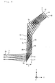
- the light that passes through an arbitrary point on the display part of the image display element 2 enters the interior of the plate-form part 5 from the upper surface 5c of the upper part of the plate-form part 5, and is then incident on the region R1 of the surface 5a of the plate-form part 5 at an angle of incidence that is greater than the critical angle, so that this light is totally reflected by the region R1.
- This light is then incident on the region R2 of the surface 5b of the plate-form part 5 at an angle of incidence that is greater than the critical angle, so that this light is totally reflected by the region R2.
- this light is then incident on the region R3 of the surface 5a of the plate-form part 5 at an angle of incidence that is greater than the critical angle, so that the light is totally reflected by the region R3.
- this light is incident on the reflective type HOE 6.
- this light is subjected to a reflective and diffractive effect that has wavelength selectivity (G light selectivity in the present working configuration), and an image focusing effect, by the reflective type HOE 6. Subsequently, this light is emitted to the outside of the plate-form part 5 from the region R4 of the surface 5a of the plate-form part 5.
- the light leaving the same location on the image display element 2 is incident on the pupil of the eye of the user, which is placed on the exit pupil P so that an enlarged false image is formed at a specified distance from the exit pupil P (1 m in the case of the present working configuration; this distance is also the same in the other working configurations described later, and may also be set, for example, at infinity).
- the light that reaches the eye of the user after being emitted from the image display element 2 and diffracted and reflected by the reflective type HOE 6 has only a G light component in accordance with the emission spectrum characteristics of the LED 3 and the wavelength selectivity of the reflective type HOE 6.
- the light rays that are emitted from an arbitrary point on the image display element 2 and that reach the center P0 of the exit pupil P (among the G light that reaches the eye of the user after being emitted from the image display element 2 and diffracted and reflected by the reflective type HOE (i.e., the light of the G wavelength region in Figure 27)) are called the chief rays with respect to the G wavelength region.
- the image quality in cases where the center of the pupil of the eye of the user deviates from the center of the exit pupil of the image combiner can be improved.
- Equation (12) shown below is satisfied. Accordingly, in the present working configuration, as will be understood from the content already described, the amount of the wavelength shift caused by the angle of view with respect to the G wavelength region width of the emission spectrum of the LED 3 is suppressed, so that the danger that a drop in the amount of light will occur in portions of the screen is eliminated. 0.2 ⁇
- Equation (13) shown below is satisfied. Accordingly, in the present working configuration, as will be understood from the content already described, the reduction in light at the ends of the angle of view can be balanced in a state that is close to the center distribution.
- the diameter of the exit pupil P is 3 mm.
- the visual field angle in the upward direction within the plane of the page in the figure is 5°.
- the visual field angle in the downward direction within the plane of the page in the figure is -5°.
- the visual field angle in the direction of depth of the page is ⁇ 6.75°.
- the screen size in the plane of the page in the figure i.e., the length between the point A1 and the point A2
- the screen size in the direction of depth of the page is 4.8 mm.
- the thickness d of the plate-form part 5 is 3.5 mm.
- the wavelength used is the wavelength width from approximately 480 nm to approximately 540 nm.
- the refractive index nd of the plate-form part 5 with respect to a wavelength of 587.56 nm (d line) is 1.596229, and the Abbe number vd is 40.4.
- the hologram is definitively defined by defining the two light beams that are used for exposure.
- the two light beams are defined by the positions of the respective light sources and either the convergence (VIR) or divergence (REA) of the beams emitted from the respective light sources.
- the coordinates of the first point light source (HV1) are designated as (HX1, HY1, HZ1), and the coordinates of the second point light source are designated as (HX2, HY2, HZ2).
- an emulsion with a thickness of 20 ⁇ m, a refractive index of 1.493 and a refractive index modulation of 0.03 is used as the emulsion that records the hologram.
- the exposure wavelength is 532 nm, and it is assumed that the shrinkage rate of the emulsion is 3.3%. Since the fluctuation in the wavelength of the playback light caused by shrinkage is in a proportional relationship, the wavelength is also shortened by 3.3%, so that the center wavelength during playback is 512 nm.
- the plane of the HOE 6 is a plane whose center is located 1.7 mm to the right along the Z axis in Figure 1 from the surface 5a, and whose orientation is rotated 30° in the clockwise direction on the plane of the page from the same direction as the Y axis:
- the HOE 6 has a phase function component in order to optimize the image focusing performance.
- the phase function is a function that defines the amount of non-spherical phase conversion other than that defined by the two pure point light sources of the HOE 6; in the optical design program Code V, this can be designated using polynomial coefficients of the X- and Y-axis components or the like.
- phase function used in Table 2 expresses the optical path difference to which the light rays incident on a point designating the HOE as a position on the XY coordinate plane are subjected as a value that is normalized by the wavelength used; if m and n are assumed to be integers, then this is determined by designating polynomial coefficients expressed by Equation (14) in general form shown below. Up to 65 such coefficients can be designated; in order, these are called C1, C2, C3, ..., C65, and when the order of the coefficients is expressed by integers j, then a correspondence is established so that the relationship expressed by Equation (15) shown below holds true between the integers m and n that indicate the order numbers of the X coordinates and Y coordinates.
- phase function is defined by the polynomial equation of Equation (16) shown below. Such a definition of the phase function is also the same for tables described later.
- j ( m + n ) 2 + m + 3 n 2 C 1 X + C 2 Y + C 3 X 2 + c 4 XY + ⁇ + C 65 Y 10
- anamorphic non-spherical surface 5c this can be defined by expressing the Z-axis coordinate value of a point (x, y) on the curved surface 5c where the optical axis of the curved surface 5c is taken as the Z coordinate axis (i.e., the amount of sag) as shown in Equation (17) below.
- Equation (17) CUX indicates the curvature radius in the X-axis direction
- CUY indicates the curvature radius in the Y-axis direction
- KX is a conical constant in the X-axis direction
- KY is a conical constant in the Y-axis direction
- AR is a fourth-order non-spherical coefficient that is rotationally symmetrical about the Z axis
- BR is a sixth-order non-spherical coefficient that is rotationally symmetrical about the Z axis
- CR is an eighth-order non-spherical coefficient that is rotationally symmetrical about the Z axis
- DR is a tenth-order non-spherical coefficient that is rotationally symmetrical about the Z axis
- AP is a rotationally asymmetrical fourth-order non-spherical coefficient
- BP is a rotationally asymmetrical sixth-order non-spherical coefficient
- CP is a rotationally asymmetrical
- HX1 0, HY1: 0.214385 ⁇ 10 +08 , HZ1: 0.155769 ⁇ 10 +08 that this is the first quadrant of yz coordinates in Figure 2, that the distance from the origin is 2.65 ⁇ 10 7 mm, and that the angle measured from the negative direction of the Z axis is 54 degrees.
- HV1 is VIR, this is convergent light, and is actually incident from the opposite direction.
- the two light sources of the HOE 6 are defined in air, the distances and angles are corrected for the refractive index and compared in cases where the HOE 6 during playback is in a medium.
- the distances are substantially infinite, no conversion is necessary. Since the distance of this light source is a distance that is close to the false image between the playback false image and the exit pupil, the dominant diffraction wavelength is constant at respective positions within the exit pupil. Instead, the dominant diffraction wavelength shifts according to the angle of view.
- the angle of incidence of the first light source with respect to the normal of the HOE is 54° in air.
- this angle is 53.1° when calculated in air. Accordingly, the angle of incidence ⁇ 1g of the exposure light on the HOE 6 and the angle of incidence ⁇ 2 of the playback light on the HOE 6 are shifted by 0.9°.
- the dominant diffraction wavelength at an angle of view of 0° is slightly shifted from the playback center wavelength of 512 nm which takes only shrinkage into account, so that this wavelength approaches the peak wavelength of 516 nm of the green emission spectrum of the light source.
- the dominant wavelengths of the diffraction efficiency of the light rays passing through the respective pupil coordinates Py of - 1.5 mm, 0 mm and +1.5 mm at the respective angles of view of -5°, 0° and +5° are as shown in Table 4 below.
- Angle of view Pupil coordinate Py -5° 0° +5° -1.5 mm 529.2 nm 516.04 nm 499.56 nm 0 mm 529.2 nm 516.04 nm 499.56 nm +1.5 mm 529.2 nm 516.04 nm 499.56 nm
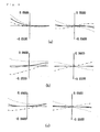
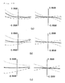
- transverse aberration diagrams used to express the image focusing performance of the optical system of the present concrete example are shown in Figures 3 and 4.
- transverse aberration diagrams for light rays of the dominant diffraction wavelength ⁇ 10 nm are shown simultaneously in one diagram for each angle of view. It is seen from Figures 3 and 4 that there is little chromatic aberration throughout the entire region within the angle of view, so that the image focusing performance is superior.
- the wavelength characteristics for the respective pupil coordinates coincide and overlap.
- Figure 5 it is shown how the dominant diffraction wavelength shifts according to the angle of view, while in Figure 6, it is shown how the dominant diffraction wavelength is not shifted according to the pupil coordinates.
- the emission spectra of the corresponding G wavelength regions are also superimposed.
- the quantity of light that reaches the eye of the observer i.e., the brightness
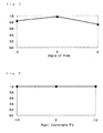
- the brightness distribution within the screen is shown in Figure 7, and the brightness distribution within the pupil plane is shown in Figure 8.
- the respective plotted points in Figure 7 correspond to the product of the peaks of the diffraction efficiency at the respective angles of view in Figure 5 and the intensity of the light emitted from the LED 3 at the corresponding peak wavelengths.
- the respective plotted points in Figure 8 correspond to the product of the peaks of the diffraction efficiency at the respective pupil coordinates in Figure 6 and the intensity of the light emitted from the LED 3 at the corresponding peak wavelengths. Furthermore, the vertical axes in Figures 7 and 8 indicate the brightness, which is normalized with the maximum brightness taken as 1.
- the respective ratios ⁇ yg / ⁇ og of the dominant diffraction wavelength ⁇ yg at angles of view of -5° and + 5° to the dominant diffraction wavelength ⁇ og at the center of the angle of view are 1.026 and 0.968, and are thus less than 0.98 and greater than 1.013, so that the conditions of Equation (10) and Equation (11) described above are satisfied.
- the intensity within the pupil plane is flat as shown in Figure 8.
- the difference between the angle ⁇ 1g of the reference light source and the angle of incidence ⁇ 2 of the optical axis of the ray tracing is 0.9°, so that the conditions of Equation (13) are satisfied.
- Figure 9 is a diagram which shows the construction of an image display device constituting a second working configuration of the present invention, and the path of the light rays (only the light rays from the image display element 2) in this image display device.
- elements that are the same as elements in Figure 1, or that correspond to elements in Figure 1 are labeled with the same symbols, and a redundant description is omitted.
- the LED 3 and reflective mirror 4 that constitute the light source are omitted from Figure 9.
- the basic difference between the present working configuration and the first working configuration described above is as follows: namely, in the first working configuration described above, the device was constructed so that the reflective type HOE 6 selectively diffracts and reflects only the G wavelength band component, while in the present working configuration, the device is constructed so that the reflective type HOE 6 selectively diffracts and reflects only the B wavelength band component.
- a B single-color LED which emits only the B wavelength region component in Figure 27 may be used as the LED 3.
- the light rays that are emitted from an arbitrary point on the image display element 2 and that reach the center P0 of the exit pupil P are called the chief rays with respect to the B wavelength region.
- the image quality in cases where the center of the pupil of the eye of the user deviates from the center of the exit pupil of the image combiner can be improved.
- Equation (20) shown below is satisfied. Accordingly, in the present working configuration, as will be understood from the content already described, the amount of the wavelength shift caused by the angle of view with respect to the B wavelength region width of the emission spectrum of the LED 3 is suppressed, so that the danger that a drop in the amount of light will occur in portions of the screen is eliminated. 0.2 ⁇
- Equation (21) shown below is satisfied. Accordingly, in the present working configuration, as will be understood from the content already described, the reduction in light at the ends of the angle of view can be balanced in a state that is close to the center distribution. 0.8° ⁇
- Equation (21) shown below is satisfied.
- the exposure wavelength of the HOE 6 is set at 476 nm.
- the diameter of the exit pupil P is 3 mm.
- the visual field angle in the upward direction within the plane of the page in the figure is 5°.
- the visual field angle in the downward direction within the plane of the page in the figure is -5°.
- the visual field angle in the direction of depth of the page is ⁇ 6.75°.
- the screen size in the plane of the page in the figure (i.e., the length between the point A1 and the point A2) is 3.6 mm.
- the screen size in the direction of depth of the page is 4.8 mm.
- the thickness d of the plate-form part 5 is 3.5 mm.
- the plate-form part 5 uses the same material as in the concrete example of the first working configuration described above.
- the plane of the HOE 6 is located at a distance of 14.7 mm from the pupil plane; of this distance, 1.7 mm is located in a medium with a refractive index of approximately 1.6. Accordingly, the length calculated in terms of air is 1.06 mm, so that the distance from the HOE 6 to the pupil plane calculated in terms of air is 14.06 mm. Consequently, the light source distance in this example is approximately twice the distance of the pupil between the false image and the pupil.
- the angle of incidence of the first light source with respect to the normal of the HOE 6 is 55.8° in air.
- this angle is 53.1° when calculated in air. Accordingly, the angle of incidence ⁇ 1b of the exposure light on the HOE 6 and the angle of incidence ⁇ 2 of the playback light on the HOE 6 are shifted by 2.7°.
- the dominant diffraction wavelength at an angle of view of 0° is shifted from the exposure wavelength of 476 nm to 460.3 nm by the shrinkage of the emulsion (assumed to be 3.3%); however, this wavelength is further slightly shifted as a result of the angular deviation of the first light source, so that this wavelength approaches the peak wavelength of 463 nm of the blue emission spectrum of the light source.
- the dominant wavelengths of the diffraction efficiency of the light rays passing through the respective pupil coordinates Py of -1.5 mm, 0 mm and +1.5 mm at the respective angles of view of -5°, 0° and +5° are as shown in Table 7 below.
- Angle of view Pupil coordinate Py -5° 0° +5° -1.5 mm 486.38 nm 469.88 nm 453.38 nm 0 mm 479.78 nm 466.58 nm 450.08 nm +1.5 mm 476.48 nm 459.98 nm 443.48 nm
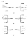
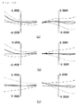
- transverse aberration diagrams used to express the image focusing performance of the optical system of the present concrete example are shown in Figures 10 and 11.
- Figures 10 and 11 transverse aberration diagrams for light rays of the dominant diffraction wavelength ⁇ 10 nm are shown simultaneously in one diagram for each angle of view. It is seen from Figures 10 and 11 that there is little chromatic aberration throughout the entire region within the angle of view, so that the image focusing performance is superior.
- the LED 3 (not shown in Figure 9) having three wavelength regions used in the present concrete example is the same as that used in the first working configuration, and has the emission spectrum shown in Figure 27.
- the emission spectra of the corresponding B wavelength regions are also superimposed.
- the quantity of light that reaches the eye of the observer i.e., the brightness
- the brightness distribution within the screen is shown in Figure 14, and the brightness distribution within the pupil plane is shown in Figure 15.
- the respective plotted points in Figure 14 correspond to the product of the peaks of the diffraction efficiency at the respective angles of view in Figure 12 and the intensity of the light emitted from the LED 3 at the corresponding peak wavelengths.
- the respective plotted points in Figure 15 correspond to the product of the peaks of the diffraction efficiency at the respective pupil coordinates in Figure 13 and the intensity of the light emitted from the LED 3 at the corresponding peak wavelengths. Furthermore, the vertical axes in Figures 14 and 15 indicate the brightness, which is normalized with the maximum brightness taken as 1.
- the respective ratios ⁇ yb / ⁇ ob of the dominant diffraction wavelength ⁇ yb at angles of view of -5° and + 5° to the dominant diffraction wavelength ⁇ ob at the center of the angle of view are 1.028 and 0.965, and are thus less than 0.98 and greater than 1.013, so that the conditions of Equation (18) and Equation (19) described above are satisfied.
- the intensity within the pupil plane is close to flat as shown in Figure 15.
- Figure 16 is a diagram which shows the construction of an image display device constituting a third working configuration of the present invention, and the path of the light rays (only the light rays from the image display element 2) in this image display device.
- elements that are the same as elements in Figure 1, or that correspond to elements in Figure 1 are labeled with the same symbols, and a redundant description is omitted.
- the LED 3 and reflective mirror 4 that constitute the light source are omitted from Figure 16.
- the basic difference between the present working configuration and the first working configuration described above is as follows: namely, in the first working configuration described above, the device was constructed so that the reflective type HOE 6 selectively diffracts and reflects only the G wavelength band component, while in the present working configuration, the device is constructed so that the reflective type HOE 6 selectively diffracts and reflects only the R wavelength band component.
- an R single-color LED which emits only the R wavelength region component in Figure 27 may be used as the LED 3.
- the light rays that are emitted from an arbitrary point on the image display element 2 and that reach the center P0 of the exit pupil P are called the chief rays with respect to the R wavelength region.
- the image quality in cases where the center of the pupil of the eye of the user deviates from the center of the exit pupil of the image combiner can be improved.
- Equation (24) shown below is satisfied. Accordingly, in the present working configuration,'as will be understood from the content already described, the amount of the wavelength shift caused by the angle of view with respect to the R wavelength region width of the emission spectrum of the LED 3 is suppressed, so that the danger that a drop in the amount of light will occur in portions of the screen is eliminated. 0.2 ⁇
- Equation (25) shown below is satisfied. Accordingly, in the present working configuration, as will be understood from the content already described, the reduction in light at the ends of the angle of view can be balanced in a state that is close to the center distribution. 0.8° ⁇
- Equation (25) shown below is satisfied.
- the exposure wavelength of the HOE 6 is set at 647 nm.
- the diameter of the exit pupil P is 3 mm.
- the visual field angle in the upward direction within the plane of the page in the figure is 5°.
- the visual field angle in the downward direction within the plane of the page in the figure is -5°.
- the visual field angle in the direction of depth of the page is ⁇ 6.75°.
- the screen size in the plane of the page in the figure (i.e., the length between the point A1 and the point A2) is 3.6 mm.
- the screen size in the direction of depth of the page is 4.8 mm.
- the thickness d of the plate-form part 5 is 3.5 mm.
- the plate-form part 5 uses the same material as in the concrete example of the first working configuration described above.
- the plane of the HOE 6 is located at a distance of 14.7 mm from the pupil plane; of this distance, 1.7 mm is located in a medium with a refractive index of approximately 1.6. Accordingly, the length calculated in terms of air is 1.06 mm, so that the distance from the HOE 6 to the pupil plane calculated in terms of air is 14.06 mm. Consequently, the light source distance in this example is a distance which is such that the light source is close to the pupil between the false image and the pupil.
- the angle of incidence of the first light source with respect to the normal of the HOE 6 is 56° in air.
- this angle is 53.1° when calculated in air. Accordingly, the angle of incidence ⁇ 1r of the exposure light on the HOE 6 and the angle of incidence ⁇ 2 of the playback light on the HOE 6 are shifted by 2.9°.
- the dominant diffraction wavelength at an angle of view of 0° is shifted from the exposure wavelength of 647 nm to 625.6 nm by the shrinkage of the emulsion (assumed to be 3.3%); however, this wavelength is further slightly shifted as a result of the angular deviation of the first light source.
- the dominant wavelengths of the diffraction efficiency of the light rays passing through the respective pupil coordinates Py of -1.5 mm, 0 mm and +1.5 mm at the respective angles of view of -5°, 0° and +5° are as shown in Table 10 below.
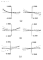
- transverse aberration diagrams used to express the image focusing performance of the optical system of the present concrete example are shown in Figures 17 and 18.
- transverse aberration diagrams for light rays of the dominant diffraction wavelength ⁇ 10 nm are shown simultaneously in one diagram for each angle of view. It is seen from Figures 17 and 18 that there is little chromatic aberration throughout the entire region within the angle of view, so that the image focusing performance is superior.
- the LED 3 (not shown in Figure 16) having three wavelength regions used in the present concrete example is the same as that used in the first working configuration, and has the emission spectrum shown in Figure 27.
- the emission spectra of the corresponding R wavelength regions are also superimposed.
- the quantity of light that reaches the eye of the observer i.e., the brightness
- the brightness distribution within the screen is shown in Figure 21, and the brightness distribution within the pupil plane is shown in Figure 22.
- the respective plotted points in Figure 21 correspond to the product of the peaks of the diffraction efficiency at the respective angles of view in Figure 19 and the intensity of the light emitted from the LED 3 at the corresponding peak wavelengths.
- the respective plotted points in Figure 22 correspond to the product of the peaks of the diffraction efficiency at the respective pupil coordinates in Figure 20 and the intensity of the light emitted from the LED 3 at the corresponding peak wavelengths.
- the respective ratios ⁇ yr / ⁇ or of the dominant diffraction wavelength ⁇ yr at angles of view of -5° and + 5° to the dominant diffraction wavelength ⁇ or at the center of the angle of view are 1.016 and 0.979, and are thus less than 0.98 and greater than 1.013, so that the conditions of Equation (22) and Equation (23) described above are satisfied.
- the intensity within the pupil plane is close to flat as shown in Figure 22.
- the difference between the angle ⁇ 1r of the reference light source and the angle of incidence ⁇ 2 of the optical axis of the ray tracing is 2.9°, so that the conditions of Equation (25) are satisfied.
- the image display device constituting a fourth working configuration of the present working configuration is a device in which the image display device constituting a concrete example of the first working configuration described above is modified as follows.
- the reflective type HOE 6 is an HOE in which the reflective type HOE of the concrete example of the first working configuration described above (G reflective type HOE), the reflective type HOE of the concrete example of the second working configuration described above (B reflective type HOE) and the reflective type HOE of the concrete example of the second working configuration described above (R reflective type HOE) are superimposed in three layers.
- the LED 3 used in the present working configuration is also an LED which has three wavelength regions, and which has the emission spectrum shown in Figure 27.
- the single display unit of the image display element may be spatially divided into three parts so that dots respectively corresponding to R, G and B are formed, and so that corresponding images are displayed, or this display unit may be divided in terms of time so that images respectively corresponding to R, G and B are switched and displayed (for example) every 1/90 second, and so that the timing of the light emission of the three wavelength regions of the LED is synchronized with this.
- the image information of the respective wavelength regions is subjected to a diffraction effect and an image focusing effect by the corresponding layers of the HOE, and full-color images are obtained by additive color mixing after this light is conducted to the pupil of the observer.
- the brightness characteristics in the image plane and the brightness characteristics in the pupil plane of the reflective type HOE 6 used in the present working configuration i.e., a reflective type HOE which has a structure in which the reflective type HOEs of the concrete examples of the first through third working configurations are superimposed are respectively shown in Figures 23 and 24.
- the vertical axes show the brightness, which is the product of the diffraction efficiency and light emission intensity of the LED; these values are normalized with the brightest value being taken as 1.
- the respective working configurations described above were examples in which a head-mounted image display device was constructed using the image combiner of the present invention.
- the respective image combiners 1 used in the respective working configurations described above could also be constructed so as to allow mounting on the ocular lens parts of camera view finders, microscopes and binoculars, or these image combiners could also be incorporated into cameras, microscopes, binoculars, or the like.
- the respective working configurations described above were examples in which the present invention was applied to a see-through type head-mounted image display device; however, the present invention can also be applied to image display devices that are not of the see-through type.
- the image display devices of the respective working configurations described above can be constructed so that light from the outside world is not incident on the image combiner 1.
- this part since the part constituting the image combiner 1 does not superimpose two images, this part cannot be called an image combiner; instead, this part constitutes a light conducting part that conducts light from the image display element 2 to the eye of the user.
- the lower portion of the plate-form part (portion below the HOE 6) in the image combiner 1 may be removed.
- such an image display device that is not of the see-through type can be installed inside the flipper part of a portable telephone in the same manner as in the case of Japanese Patent Application Kokai No. 2001-264682.
Landscapes
- Physics & Mathematics (AREA)
- General Physics & Mathematics (AREA)
- Optics & Photonics (AREA)
- Diffracting Gratings Or Hologram Optical Elements (AREA)
- Lenses (AREA)
Applications Claiming Priority (3)
| Application Number | Priority Date | Filing Date | Title |
|---|---|---|---|
| JP2002218184 | 2002-07-26 | ||
| JP2002218184A JP3867634B2 (ja) | 2002-07-26 | 2002-07-26 | イメージコンバイナ及び画像表示装置 |
| PCT/JP2003/009430 WO2004011986A1 (ja) | 2002-07-26 | 2003-07-25 | イメージコンバイナ及び画像表示装置 |
Publications (2)
| Publication Number | Publication Date |
|---|---|
| EP1536268A1 true EP1536268A1 (de) | 2005-06-01 |
| EP1536268A4 EP1536268A4 (de) | 2006-03-08 |
Family
ID=31184669
Family Applications (1)
| Application Number | Title | Priority Date | Filing Date |
|---|---|---|---|
| EP03771325A Withdrawn EP1536268A4 (de) | 2002-07-26 | 2003-07-25 | Bildkombinierer und bildanzeigeeinheit |
Country Status (6)
| Country | Link |
|---|---|
| US (1) | US7072085B2 (de) |
| EP (1) | EP1536268A4 (de) |
| JP (1) | JP3867634B2 (de) |
| CN (1) | CN1672082A (de) |
| AU (1) | AU2003252686A1 (de) |
| WO (1) | WO2004011986A1 (de) |
Cited By (6)
| Publication number | Priority date | Publication date | Assignee | Title |
|---|---|---|---|---|
| WO2007031991A3 (en) * | 2005-09-14 | 2007-06-07 | Mirage Innovations Ltd | Diffractive optical device and system |
| EP1942364A1 (de) * | 2005-09-14 | 2008-07-09 | Mirage Innovations Ltd. | Diffraktives optisches Relais und Herstellungsverfahren dafür |
| WO2008090000A1 (de) * | 2007-01-25 | 2008-07-31 | Rodenstock Gmbh | Brille und brillenglas zur dateneinspiegelung |
| US7573640B2 (en) | 2005-04-04 | 2009-08-11 | Mirage Innovations Ltd. | Multi-plane optical apparatus |
| EP2133727A1 (de) * | 2008-06-10 | 2009-12-16 | Sony Corporation | Optische Vorrichtung und virtuelle Bildanzeige |
| USRE42992E1 (en) | 2003-02-19 | 2011-12-06 | Mirage Innovations Ltd. | Chromatic planar optic display system |
Families Citing this family (69)
| Publication number | Priority date | Publication date | Assignee | Title |
|---|---|---|---|---|
| WO2004061519A1 (ja) | 2002-12-24 | 2004-07-22 | Nikon Corporation | ヘッドマウントディスプレイ |
| EP1619536B1 (de) | 2003-04-28 | 2022-02-16 | Nikon Corporation | Bildkombinierer und bildanzeige |
| JP4320713B2 (ja) * | 2003-05-06 | 2009-08-26 | コニカミノルタホールディングス株式会社 | 映像表示装置 |
| US7418170B2 (en) * | 2004-03-29 | 2008-08-26 | Sony Corporation | Optical device and virtual image display device |
| US7405881B2 (en) | 2005-05-30 | 2008-07-29 | Konica Minolta Holdings, Inc. | Image display apparatus and head mount display |
| GB0522968D0 (en) | 2005-11-11 | 2005-12-21 | Popovich Milan M | Holographic illumination device |
| GB0718706D0 (en) | 2007-09-25 | 2007-11-07 | Creative Physics Ltd | Method and apparatus for reducing laser speckle |
| JP2007304227A (ja) * | 2006-05-10 | 2007-11-22 | Konica Minolta Holdings Inc | 映像表示装置および映像撮影装置 |
| US7483215B2 (en) * | 2006-08-28 | 2009-01-27 | Genie Lens Technologies, Llc | Reflective imaging assembly for displaying interlaced images |
| JP4267030B2 (ja) * | 2006-12-26 | 2009-05-27 | オリンパス株式会社 | 顕微鏡装置、コントローラ、及びプログラム |
| JP5003291B2 (ja) | 2007-05-31 | 2012-08-15 | コニカミノルタホールディングス株式会社 | 映像表示装置 |
| WO2009050504A1 (en) * | 2007-10-18 | 2009-04-23 | Bae Systems Plc | Improvements in or relating to head mounted display systems |
| US8228576B2 (en) | 2008-08-11 | 2012-07-24 | Dai Nippon Printing Co., Ltd. | Transmission type optical element and anti-forgery volume hologram |
| US8638483B2 (en) * | 2008-09-17 | 2014-01-28 | Konica Minolta Holdings, Inc. | Image display device and head-mounted display |
| US10274660B2 (en) | 2008-11-17 | 2019-04-30 | Luminit, Llc | Holographic substrate-guided wave-based see-through display |
| JPWO2010061835A1 (ja) * | 2008-11-26 | 2012-04-26 | コニカミノルタオプト株式会社 | 映像表示装置およびヘッドマウントディスプレイ |
| US9335604B2 (en) | 2013-12-11 | 2016-05-10 | Milan Momcilo Popovich | Holographic waveguide display |
| US11726332B2 (en) | 2009-04-27 | 2023-08-15 | Digilens Inc. | Diffractive projection apparatus |
| WO2010134374A1 (ja) * | 2009-05-20 | 2010-11-25 | コニカミノルタオプト株式会社 | 映像表示装置、ヘッドマウントディスプレイおよびヘッドアップディスプレイ |
| US9274349B2 (en) | 2011-04-07 | 2016-03-01 | Digilens Inc. | Laser despeckler based on angular diversity |
| WO2016020630A2 (en) | 2014-08-08 | 2016-02-11 | Milan Momcilo Popovich | Waveguide laser illuminator incorporating a despeckler |
| US20140204455A1 (en) | 2011-08-24 | 2014-07-24 | Milan Momcilo Popovich | Wearable data display |
| US10670876B2 (en) | 2011-08-24 | 2020-06-02 | Digilens Inc. | Waveguide laser illuminator incorporating a despeckler |
| US20150010265A1 (en) | 2012-01-06 | 2015-01-08 | Milan, Momcilo POPOVICH | Contact image sensor using switchable bragg gratings |
| CN106125308B (zh) | 2012-04-25 | 2019-10-25 | 罗克韦尔柯林斯公司 | 用于显示图像的装置和方法 |
| US9456744B2 (en) | 2012-05-11 | 2016-10-04 | Digilens, Inc. | Apparatus for eye tracking |
| US10061069B2 (en) | 2012-06-22 | 2018-08-28 | Luminit Llc | Method for design and manufacturing of optics for holographic sight |
| US9933684B2 (en) | 2012-11-16 | 2018-04-03 | Rockwell Collins, Inc. | Transparent waveguide display providing upper and lower fields of view having a specific light output aperture configuration |
| US10209517B2 (en) | 2013-05-20 | 2019-02-19 | Digilens, Inc. | Holographic waveguide eye tracker |
| WO2015015138A1 (en) | 2013-07-31 | 2015-02-05 | Milan Momcilo Popovich | Method and apparatus for contact image sensing |
| US10359736B2 (en) | 2014-08-08 | 2019-07-23 | Digilens Inc. | Method for holographic mastering and replication |
| US10241330B2 (en) | 2014-09-19 | 2019-03-26 | Digilens, Inc. | Method and apparatus for generating input images for holographic waveguide displays |
| WO2016046514A1 (en) | 2014-09-26 | 2016-03-31 | LOKOVIC, Kimberly, Sun | Holographic waveguide opticaltracker |
| EP3245444B1 (de) | 2015-01-12 | 2021-09-08 | DigiLens Inc. | Umweltisolierte wellenleiteranzeige |
| US20180275402A1 (en) | 2015-01-12 | 2018-09-27 | Digilens, Inc. | Holographic waveguide light field displays |
| JP6867947B2 (ja) | 2015-01-20 | 2021-05-12 | ディジレンズ インコーポレイテッド | ホログラフィック導波路ライダー |
| US9632226B2 (en) | 2015-02-12 | 2017-04-25 | Digilens Inc. | Waveguide grating device |
| US10459145B2 (en) | 2015-03-16 | 2019-10-29 | Digilens Inc. | Waveguide device incorporating a light pipe |
| US10591756B2 (en) | 2015-03-31 | 2020-03-17 | Digilens Inc. | Method and apparatus for contact image sensing |
| CN108474945B (zh) | 2015-10-05 | 2021-10-01 | 迪吉伦斯公司 | 波导显示器 |
| EP3398007B1 (de) | 2016-02-04 | 2024-09-11 | DigiLens, Inc. | Optischer wellenleitertracker |
| WO2017162999A1 (en) | 2016-03-24 | 2017-09-28 | Popovich Milan Momcilo | Method and apparatus for providing a polarization selective holographic waveguide device |
| US10890707B2 (en) | 2016-04-11 | 2021-01-12 | Digilens Inc. | Holographic waveguide apparatus for structured light projection |
| WO2018102834A2 (en) | 2016-12-02 | 2018-06-07 | Digilens, Inc. | Waveguide device with uniform output illumination |
| US20180188685A1 (en) * | 2016-12-30 | 2018-07-05 | Luminit, Llc | Monolithic Optical System for Light Propagation in Confined Spaces and Method of Fabrication |
| US10545346B2 (en) | 2017-01-05 | 2020-01-28 | Digilens Inc. | Wearable heads up displays |
| US10930710B2 (en) * | 2017-05-04 | 2021-02-23 | Apple Inc. | Display with nanostructure angle-of-view adjustment structures |
| WO2019079350A2 (en) | 2017-10-16 | 2019-04-25 | Digilens, Inc. | SYSTEMS AND METHODS FOR MULTIPLYING THE IMAGE RESOLUTION OF A PIXÉLISÉ DISPLAY |
| JP7250799B2 (ja) | 2018-01-08 | 2023-04-03 | ディジレンズ インコーポレイテッド | 光学導波管を加工するための方法 |
| US10914950B2 (en) | 2018-01-08 | 2021-02-09 | Digilens Inc. | Waveguide architectures and related methods of manufacturing |
| KR102819207B1 (ko) | 2018-01-08 | 2025-06-11 | 디지렌즈 인코포레이티드. | 도파관 셀을 제조하기 위한 시스템 및 방법 |
| WO2019135796A1 (en) | 2018-01-08 | 2019-07-11 | Digilens, Inc. | Systems and methods for high-throughput recording of holographic gratings in waveguide cells |
| CN112088332B (zh) | 2018-03-16 | 2024-11-29 | 迪吉伦斯公司 | 包含双折射控制的全息波导及用于它们的制造的方法 |
| US11402801B2 (en) | 2018-07-25 | 2022-08-02 | Digilens Inc. | Systems and methods for fabricating a multilayer optical structure |
| US20200225471A1 (en) | 2019-01-14 | 2020-07-16 | Digilens Inc. | Holographic Waveguide Display with Light Control Layer |
| WO2020163524A1 (en) | 2019-02-05 | 2020-08-13 | Digilens Inc. | Methods for compensating for optical surface nonuniformity |
| US20220283377A1 (en) | 2019-02-15 | 2022-09-08 | Digilens Inc. | Wide Angle Waveguide Display |
| KR102866596B1 (ko) | 2019-02-15 | 2025-09-29 | 디지렌즈 인코포레이티드. | 일체형 격자를 이용하여 홀로그래픽 도파관 디스플레이를 제공하기 위한 방법 및 장치 |
| KR20210134763A (ko) | 2019-03-12 | 2021-11-10 | 디지렌즈 인코포레이티드. | 홀로그래픽 도파관 백라이트 및 관련된 제조 방법 |
| WO2020247930A1 (en) | 2019-06-07 | 2020-12-10 | Digilens Inc. | Waveguides incorporating transmissive and reflective gratings and related methods of manufacturing |
| US11681143B2 (en) | 2019-07-29 | 2023-06-20 | Digilens Inc. | Methods and apparatus for multiplying the image resolution and field-of-view of a pixelated display |
| JP2021021879A (ja) * | 2019-07-30 | 2021-02-18 | セイコーエプソン株式会社 | 光学素子及び画像表示装置 |
| CN112306229A (zh) * | 2019-08-02 | 2021-02-02 | 佳能株式会社 | 电子装置、控制方法和计算机可读介质 |
| CN114450608A (zh) | 2019-08-29 | 2022-05-06 | 迪吉伦斯公司 | 真空布拉格光栅和制造方法 |
| JP7484599B2 (ja) * | 2020-09-09 | 2024-05-16 | 日本精機株式会社 | ヘッドアップディスプレイ |
| EP4252048A4 (de) | 2020-12-21 | 2024-10-16 | Digilens Inc. | Augenglimmunterdrückung in wellenleiterbasierten anzeigen |
| US12399326B2 (en) | 2021-01-07 | 2025-08-26 | Digilens Inc. | Grating structures for color waveguides |
| JP2024508926A (ja) | 2021-03-05 | 2024-02-28 | ディジレンズ インコーポレイテッド | 真空周期的構造体および製造の方法 |
| US20240184245A1 (en) * | 2021-03-19 | 2024-06-06 | Sony Group Corporation | Display device |
Family Cites Families (13)
| Publication number | Priority date | Publication date | Assignee | Title |
|---|---|---|---|---|
| US4655540A (en) * | 1985-04-23 | 1987-04-07 | Flight Dynamics, Inc. | Holographic optical display system with optimum brightness uniformity |
| DE3532120A1 (de) * | 1985-09-10 | 1987-03-19 | Ver Glaswerke Gmbh | Windschutzscheibe mit einer reflektierenden einrichtung zur einspiegelung von optischen signalen in das gesichtsfeld des fahrers |
| JP2585717B2 (ja) * | 1988-06-03 | 1997-02-26 | キヤノン株式会社 | 表示装置 |
| JPH01306886A (ja) * | 1988-06-03 | 1989-12-11 | Canon Inc | 体積位相型回折格子 |
| US5680231A (en) * | 1995-06-06 | 1997-10-21 | Hughes Aircraft Company | Holographic lenses with wide angular and spectral bandwidths for use in a color display device |
| JPH1164781A (ja) | 1997-08-14 | 1999-03-05 | Fuji Xerox Co Ltd | 網膜直接描画装置 |
| JP4063922B2 (ja) * | 1997-08-25 | 2008-03-19 | 富士フイルム株式会社 | 光ビーム走査装置 |
| JP3885386B2 (ja) | 1998-10-20 | 2007-02-21 | コニカミノルタオプト株式会社 | ホログラム素子の製造方法 |
| JP4691744B2 (ja) | 1999-06-11 | 2011-06-01 | コニカミノルタホールディングス株式会社 | 映像表示装置 |
| JP4325064B2 (ja) | 2000-03-17 | 2009-09-02 | コニカミノルタホールディングス株式会社 | 情報表示光学系 |
| JP4269482B2 (ja) * | 2000-04-27 | 2009-05-27 | コニカミノルタホールディングス株式会社 | 映像表示装置 |
| JP2002122783A (ja) * | 2000-10-13 | 2002-04-26 | Olympus Optical Co Ltd | 観察光学系及び撮像光学系及びそれを用いた装置 |
| JP2002258488A (ja) | 2001-03-05 | 2002-09-11 | Minolta Co Ltd | ホログラフィック光学素子の製造における露光方法及び露光装置 |
-
2002
- 2002-07-26 JP JP2002218184A patent/JP3867634B2/ja not_active Expired - Fee Related
-
2003
- 2003-07-25 EP EP03771325A patent/EP1536268A4/de not_active Withdrawn
- 2003-07-25 CN CN03817763.3A patent/CN1672082A/zh active Pending
- 2003-07-25 WO PCT/JP2003/009430 patent/WO2004011986A1/ja not_active Ceased
- 2003-07-25 AU AU2003252686A patent/AU2003252686A1/en not_active Abandoned
-
2005
- 2005-01-10 US US11/032,202 patent/US7072085B2/en not_active Expired - Fee Related
Cited By (11)
| Publication number | Priority date | Publication date | Assignee | Title |
|---|---|---|---|---|
| USRE42992E1 (en) | 2003-02-19 | 2011-12-06 | Mirage Innovations Ltd. | Chromatic planar optic display system |
| US7573640B2 (en) | 2005-04-04 | 2009-08-11 | Mirage Innovations Ltd. | Multi-plane optical apparatus |
| WO2007031991A3 (en) * | 2005-09-14 | 2007-06-07 | Mirage Innovations Ltd | Diffractive optical device and system |
| EP1942364A1 (de) * | 2005-09-14 | 2008-07-09 | Mirage Innovations Ltd. | Diffraktives optisches Relais und Herstellungsverfahren dafür |
| WO2008090000A1 (de) * | 2007-01-25 | 2008-07-31 | Rodenstock Gmbh | Brille und brillenglas zur dateneinspiegelung |
| US8177361B2 (en) | 2007-01-25 | 2012-05-15 | Rodenstock Gmbh | Spectacle glass and spectacle lens for data reflection |
| EP2133727A1 (de) * | 2008-06-10 | 2009-12-16 | Sony Corporation | Optische Vorrichtung und virtuelle Bildanzeige |
| US8325166B2 (en) | 2008-06-10 | 2012-12-04 | Sony Corporation | Optical device and virtual image display device including volume hologram gratings |
| US8810878B2 (en) | 2008-06-10 | 2014-08-19 | Sony Corporation | Optical device and virtual image display |
| US9383722B2 (en) | 2008-06-10 | 2016-07-05 | Sony Corporation | Optical device and virtual image display |
| US10025100B2 (en) | 2008-06-10 | 2018-07-17 | Sony Corporation | Optical device and virtual image display |
Also Published As
| Publication number | Publication date |
|---|---|
| WO2004011986A1 (ja) | 2004-02-05 |
| US7072085B2 (en) | 2006-07-04 |
| CN1672082A (zh) | 2005-09-21 |
| US20050141066A1 (en) | 2005-06-30 |
| JP2004061731A (ja) | 2004-02-26 |
| EP1536268A4 (de) | 2006-03-08 |
| JP3867634B2 (ja) | 2007-01-10 |
| AU2003252686A1 (en) | 2004-02-16 |
Similar Documents
| Publication | Publication Date | Title |
|---|---|---|
| EP1536268A1 (de) | Bildkombinierer und bildanzeigeeinheit | |
| US7085027B2 (en) | Image combiner and image display | |
| EP1542062A1 (de) | Bildkombinierer und bildanzeigeeinheit | |
| CN105929535B (zh) | 图像显示装置 | |
| JP5534009B2 (ja) | 映像表示装置、ヘッドマウントディスプレイおよびヘッドアップディスプレイ | |
| US6922267B2 (en) | Image display apparatus | |
| US8035872B2 (en) | Image combiner and image display device | |
| JP5732808B2 (ja) | 虚像表示装置 | |
| US7081999B2 (en) | Image display apparatus and head mounted display using it | |
| JP2002311379A (ja) | 観察光学系 | |
| JP2010262232A (ja) | 映像表示装置およびヘッドマウントディスプレイ | |
| US20180373038A1 (en) | Optics of wearable display devices | |
| JP2012013908A (ja) | 映像表示装置およびヘッドマウントディスプレイ | |
| JP4717196B2 (ja) | 画像観察装置および画像観察システム | |
| JP2005241825A (ja) | 画像表示装置 | |
| EP3982189A1 (de) | Bildanzeigevorrichtung und anzeigevorrichtung | |
| WO2011001787A1 (ja) | 映像表示装置、hmdおよびhud | |
| JP2010145721A (ja) | 光路コンバイナ、映像表示装置およびヘッドマウントディスプレイ | |
| US20250102809A1 (en) | Display device | |
| US20230305305A1 (en) | Compensated diffractive waveguide for off-axis in-coupling and viewing | |
| JP2004325985A (ja) | 画像表示装置 | |
| WO2010122854A1 (ja) | 映像表示装置、ヘッドマウントディスプレイおよびヘッドアップディスプレイ | |
| JP2003140079A (ja) | イメージコンバイナ及び画像表示装置 | |
| US20250102806A1 (en) | Virtual image display device and optical unit | |
| EP4411453A1 (de) | Optisches system, virtuelle bildanzeigevorrichtung und kopfmontierte anzeige |
Legal Events
| Date | Code | Title | Description |
|---|---|---|---|
| PUAI | Public reference made under article 153(3) epc to a published international application that has entered the european phase |
Free format text: ORIGINAL CODE: 0009012 |
|
| 17P | Request for examination filed |
Effective date: 20050121 |
|
| AK | Designated contracting states |
Kind code of ref document: A1 Designated state(s): AT BE BG CH CY CZ DE DK EE ES FI FR GB GR HU IE IT LI LU MC NL PT RO SE SI SK TR |
|
| AX | Request for extension of the european patent |
Extension state: AL LT LV MK |
|
| DAX | Request for extension of the european patent (deleted) | ||
| A4 | Supplementary search report drawn up and despatched |
Effective date: 20060123 |
|
| 17Q | First examination report despatched |
Effective date: 20060823 |
|
| STAA | Information on the status of an ep patent application or granted ep patent |
Free format text: STATUS: THE APPLICATION IS DEEMED TO BE WITHDRAWN |
|
| 18D | Application deemed to be withdrawn |
Effective date: 20070103 |