EP1530244A2 - Circuit de contrôle de sautes de courant comprenant un composant à transition métal-isolateur abrupte - Google Patents
Circuit de contrôle de sautes de courant comprenant un composant à transition métal-isolateur abrupte Download PDFInfo
- Publication number
- EP1530244A2 EP1530244A2 EP04253582A EP04253582A EP1530244A2 EP 1530244 A2 EP1530244 A2 EP 1530244A2 EP 04253582 A EP04253582 A EP 04253582A EP 04253582 A EP04253582 A EP 04253582A EP 1530244 A2 EP1530244 A2 EP 1530244A2
- Authority
- EP
- European Patent Office
- Prior art keywords
- phase transition
- current
- abrupt metal
- insulator phase
- insulator
- Prior art date
- Legal status (The legal status is an assumption and is not a legal conclusion. Google has not performed a legal analysis and makes no representation as to the accuracy of the status listed.)
- Withdrawn
Links
- 239000012212 insulator Substances 0.000 title claims abstract description 85
- 230000007704 transition Effects 0.000 title claims abstract description 67
- 230000005684 electric field Effects 0.000 claims abstract description 6
- 239000000463 material Substances 0.000 claims description 7
- 239000010409 thin film Substances 0.000 claims description 5
- XHCLAFWTIXFWPH-UHFFFAOYSA-N [O-2].[O-2].[O-2].[O-2].[O-2].[V+5].[V+5] Chemical compound [O-2].[O-2].[O-2].[O-2].[O-2].[V+5].[V+5] XHCLAFWTIXFWPH-UHFFFAOYSA-N 0.000 claims description 2
- 239000010408 film Substances 0.000 claims description 2
- 229910001935 vanadium oxide Inorganic materials 0.000 claims description 2
- 229910021542 Vanadium(IV) oxide Inorganic materials 0.000 description 6
- GRUMUEUJTSXQOI-UHFFFAOYSA-N vanadium dioxide Chemical compound O=[V]=O GRUMUEUJTSXQOI-UHFFFAOYSA-N 0.000 description 6
- 239000000758 substrate Substances 0.000 description 4
- 230000005669 field effect Effects 0.000 description 3
- XUIMIQQOPSSXEZ-UHFFFAOYSA-N Silicon Chemical compound [Si] XUIMIQQOPSSXEZ-UHFFFAOYSA-N 0.000 description 2
- 230000005540 biological transmission Effects 0.000 description 2
- 230000007423 decrease Effects 0.000 description 2
- 238000010586 diagram Methods 0.000 description 2
- 229910052751 metal Inorganic materials 0.000 description 2
- 239000002184 metal Substances 0.000 description 2
- TWNQGVIAIRXVLR-UHFFFAOYSA-N oxo(oxoalumanyloxy)alumane Chemical compound O=[Al]O[Al]=O TWNQGVIAIRXVLR-UHFFFAOYSA-N 0.000 description 2
- 229910052710 silicon Inorganic materials 0.000 description 2
- 239000010703 silicon Substances 0.000 description 2
- 239000002800 charge carrier Substances 0.000 description 1
- 230000003247 decreasing effect Effects 0.000 description 1
- 229910044991 metal oxide Inorganic materials 0.000 description 1
- 150000004706 metal oxides Chemical class 0.000 description 1
- 238000000034 method Methods 0.000 description 1
- 239000004065 semiconductor Substances 0.000 description 1
Images


Classifications
-
- H—ELECTRICITY
- H10—SEMICONDUCTOR DEVICES; ELECTRIC SOLID-STATE DEVICES NOT OTHERWISE PROVIDED FOR
- H10N—ELECTRIC SOLID-STATE DEVICES NOT OTHERWISE PROVIDED FOR
- H10N70/00—Solid-state devices having no potential barriers, and specially adapted for rectifying, amplifying, oscillating or switching
- H10N70/801—Constructional details of multistable switching devices
- H10N70/821—Device geometry
- H10N70/823—Device geometry adapted for essentially horizontal current flow, e.g. bridge type devices
-
- H—ELECTRICITY
- H10—SEMICONDUCTOR DEVICES; ELECTRIC SOLID-STATE DEVICES NOT OTHERWISE PROVIDED FOR
- H10N—ELECTRIC SOLID-STATE DEVICES NOT OTHERWISE PROVIDED FOR
- H10N70/00—Solid-state devices having no potential barriers, and specially adapted for rectifying, amplifying, oscillating or switching
-
- H—ELECTRICITY
- H01—ELECTRIC ELEMENTS
- H01L—SEMICONDUCTOR DEVICES NOT COVERED BY CLASS H10
- H01L29/00—Semiconductor devices specially adapted for rectifying, amplifying, oscillating or switching and having potential barriers; Capacitors or resistors having potential barriers, e.g. a PN-junction depletion layer or carrier concentration layer; Details of semiconductor bodies or of electrodes thereof ; Multistep manufacturing processes therefor
- H01L29/66—Types of semiconductor device ; Multistep manufacturing processes therefor
- H01L29/68—Types of semiconductor device ; Multistep manufacturing processes therefor controllable by only the electric current supplied, or only the electric potential applied, to an electrode which does not carry the current to be rectified, amplified or switched
- H01L29/76—Unipolar devices, e.g. field effect transistors
- H01L29/772—Field effect transistors
- H01L29/78—Field effect transistors with field effect produced by an insulated gate
-
- H—ELECTRICITY
- H10—SEMICONDUCTOR DEVICES; ELECTRIC SOLID-STATE DEVICES NOT OTHERWISE PROVIDED FOR
- H10N—ELECTRIC SOLID-STATE DEVICES NOT OTHERWISE PROVIDED FOR
- H10N70/00—Solid-state devices having no potential barriers, and specially adapted for rectifying, amplifying, oscillating or switching
- H10N70/20—Multistable switching devices, e.g. memristors
-
- H—ELECTRICITY
- H10—SEMICONDUCTOR DEVICES; ELECTRIC SOLID-STATE DEVICES NOT OTHERWISE PROVIDED FOR
- H10N—ELECTRIC SOLID-STATE DEVICES NOT OTHERWISE PROVIDED FOR
- H10N70/00—Solid-state devices having no potential barriers, and specially adapted for rectifying, amplifying, oscillating or switching
- H10N70/801—Constructional details of multistable switching devices
- H10N70/821—Device geometry
- H10N70/826—Device geometry adapted for essentially vertical current flow, e.g. sandwich or pillar type devices
-
- H—ELECTRICITY
- H10—SEMICONDUCTOR DEVICES; ELECTRIC SOLID-STATE DEVICES NOT OTHERWISE PROVIDED FOR
- H10N—ELECTRIC SOLID-STATE DEVICES NOT OTHERWISE PROVIDED FOR
- H10N70/00—Solid-state devices having no potential barriers, and specially adapted for rectifying, amplifying, oscillating or switching
- H10N70/801—Constructional details of multistable switching devices
- H10N70/881—Switching materials
- H10N70/883—Oxides or nitrides
- H10N70/8833—Binary metal oxides, e.g. TaOx
Definitions
- the present invention relates to a current-jump-control circuit including an abrupt metal-insulator phase transition device.
- a Mott field effect transistor which uses a Mott insulator as the channel layer. Since the Mott FET utilizes a metal-insulator phase transition that is successively generated, it is necessary to add electrons or holes to be used as a charge carrier until a metallic characteristic appears most well, which causes a limitation that the added charge should be in a high concentration state. Accordingly, a method using an insulator that shows an abrupt metal-insulator phase transition characteristic of a current jump under a constant condition has been recently proposed instead of an insulator showing a continuous metal-insulator phase transition, and is disclosed in US Patent No. 6,624,463. A field effect transistor disclosed in US Patent No. 6,624,463 shows an abrupt metal-insulator phase transition characteristic of a current jump induced by doping of a small hole concentration.
- FIG. 1 is a graph showing electric field-current density characteristic of a current jump of a device manufactured using a material showing such an abrupt metal-insulator phase transition.
- the abrupt metal-insulator phase transition device when an electric field (E field ) of a predetermined level, for instance, of 7 MV/m is applied to both terminals of the device, the abrupt metal-insulator phase transition device is abruptly phase-transited from an insulator to a metal, so that a large amount of current flows through both terminals of the device.
- E field electric field
- the device may not endure against the large current and may be failed.
- a device which causes an abrupt metal-insulator phase transition when an electric field above a critical value is applied, is defined as "abrupt metal-insulator phase transition device.”
- an abrupt metal-insulator phase transition may generate a large amount of current (current jump) abruptly.
- the abrupt metal-insulator phase transition device needs a control circuit that can control the current jump so as to endure this large amount of current.
- the present invention provides a current jump control circuit including an abrupt metal-insulator phase transition device that can properly control a large amount of current flowing through the abrupt metal-insulator phase transition device to prevent the abrupt metal-insulator phase transition device from being failed.
- a current control circuit including an abrupt metal-insulator phase transition device, comprising: a source; the abrupt metal-insulator phase transition device including first and second electrodes connected to the source, and showing an abrupt metal-insulator phase transition characteristic of a current jump when an electric field is applied between the first electrode and the second electrode; and a resistive element which is connected between the source and the abrupt metal-insulator phase transition device and is able to control a current jump flowing through the abrupt metal-insulator phase transition device.
- the resistive element may be connected in series with the abrupt metal-insulator phase transition device.
- the resistive element may be a resistor.
- the resistive element may be a variable resistor.
- the resistive element may be a planar type device pattern that can be used as a resistor.
- the resistive element may be an internal resistance material in the inhomogeneous phase-transition thin-film insulator that can be used as a resistor.
- the abrupt metal-insulator phase transition device may have a structure that an insulator film having an abrupt metal-insulator phase transition characteristic is disposed between the first electrode and the second electrode.
- the insulator may comprise a vanadium oxide.
- FIG. 2 is a diagram of a current control circuit including an abrupt metal-insulator phase transition device according to the present invention
- FIG. 3 is a sectional view of the abrupt metal-insulator phase transition device of FIG. 2.
- a current control circuit includes a source 100, an abrupt metal-insulator phase transition device 200, and a resistive element 300.
- the source 100 may be a direct current (DC) source or an alternating current (AC) source.
- DC direct current
- AC alternating current
- the abrupt metal-insulator phase transition device 200 is, as shown in FIG. 3A or 3B, provided with a thin film type insulator 220 having an abrupt metal-insulator phase transition characteristic of a current jump, and first and second electrodes 230 and 240 disposed at both sides of the thin film type insulator 220.
- the device 200 includes a substrate 210, which is made of sapphire (Al 2 O 3 ) or silicon (Si). It will be apparent that the substrate 210 can be made of a material other than the aforementioned materials.
- the insulator 220 contains Vanadium dioxide (VO 2 ).
- the resistive element 300 is an element that can function as a controllable resistance, and includes a resistor representatively. In particular, the resistive element 300 may be a variable resistor that can control a resistance thereof with ease. Sometimes, the resistive element 300 may be a planar device pattern that can be used as a resistor.
- This planar device pattern has a property that its resistance is proportional to its length, and shows a resistance characteristic by connecting meander type transmission lines, various planar type inductors (AC resistances) and the like using the property of the planar device pattern.
- the resistance is controllable by adjusting the length of the transmission lines or the number of the planar type devices, etc.
- the resistive element 300 maybe an internal resistance material in the inhomogeneous phase-transition thin-film insulator.
- the insulator 220 of the abrupt metal-insulator phase transition device 200 forms a current flow path (expressed by an arrow of a dotted line in FIG. 3) on a surface thereof while experiencing an abrupt metal-insulator phase transition phenomenon.
- a large amount of jump current flows from the first electrode 230 to the second electrode 240.
- the current amount is reduced, i.e., is controlled, by the resistive element 300, so that the current flows by such an amount that the abrupt metal-insulator phase transition device 200 is not failed.
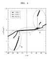
- FIG. 4 is a graph showing the resistance dependence of the current jump of voltage-current density characteristic of a current control circuit including an abrupt metal-insulator phase transition device according to a first embodiment of the present invention.
- a horizontal axis represents a voltage (V) applied between the first electrode 230 and the second electrode 240
- a vertical axis is a current density (J) between the first electrode 230 and the second electrode 240.
- the abrupt metal-insulator phase transition device 200 used in the test of FIG. 4 is a device having the sapphire (Al 2 O 3 ) substrate 210 and the vanadium dioxide (VO 2 ) insulator 220, and has a channel length of 5 ⁇ m between the first electrode 230 and the second electrode 240 and a channel width of 25 ⁇ m.
- Al 2 O 3 the sapphire
- VO 2 vanadium dioxide
- a line indicated by a reference symbol '•' corresponds to a case that the resistance (R) of the resistive element 300 is 1.0 k ⁇
- a line indicated by a reference symbol ' ⁇ ' corresponds to a case that the resistance (R) of the resistive element is 2.5 k ⁇
- a line indicated by a reference symbol ' ⁇ ' corresponds to a case that the resistance (R) of the resistive element 300 is 5.0 k ⁇ .
- FIG. 5 is a graph showing the resistance dependence of the current jump of voltage-current density characteristic of a current control circuit including an abrupt metal-insulator phase transition device according to a second embodiment of the present invention.
- a horizontal axis represents a voltage (V) applied between the first electrode 230 and the second electrode 240
- a vertical axis is a current density (J) between the first electrode 230 and the second electrode 240.
- the abrupt metal-insulator phase transition device 200 used in the test of FIG. 5 is a device using the silicon (Si) substrate 210 and the vanadium dioxide (VO 2 ) insulator 220, and has a channel length of 5 ⁇ m between the first electrode 230 and the second electrode 240 and a channel width of 25 ⁇ m.
- Si silicon
- VO 2 vanadium dioxide
- a line indicated by a reference symbol ' ⁇ ' corresponds to a case that the resistance (R) of the resistive element 300 is 110 ⁇
- a line indicated by a reference symbol '•' corresponds to a case that the resistance (R) of the resistive element 300 is 340 ⁇
- a line indicated by a reference symbol ' ⁇ ' corresponds to a case that the resistance (R) of the resistive element is 1.0 k ⁇
- a line indicated by a reference symbol ' ⁇ ' corresponds to a case that the resistance (R) of the resistive element 300 is 5.0 k ⁇
- a line indicated by a reference symbol ' ⁇ ' corresponds to a case that the resistance (R) of the resistive element 300 is 10 k ⁇ .
- the resistive element connected in series to the abrupt metal-insulator phase transition device suppresses a magnitude of the current jump, so that the abrupt metal-insulator phase transition device can be prevented from being failed and thus the current control circuit can be applied in various application fields.
Landscapes
- Engineering & Computer Science (AREA)
- Microelectronics & Electronic Packaging (AREA)
- Power Engineering (AREA)
- Physics & Mathematics (AREA)
- Ceramic Engineering (AREA)
- Condensed Matter Physics & Semiconductors (AREA)
- General Physics & Mathematics (AREA)
- Computer Hardware Design (AREA)
- Thermistors And Varistors (AREA)
- Semiconductor Memories (AREA)
- Emergency Protection Circuit Devices (AREA)
- Semiconductor Integrated Circuits (AREA)
Applications Claiming Priority (2)
| Application Number | Priority Date | Filing Date | Title |
|---|---|---|---|
| KR1020030078333A KR100576704B1 (ko) | 2003-11-06 | 2003-11-06 | 급격한 금속-절연체 상전이형 소자를 포함하는 전류제어회로 |
| KR2003078333 | 2003-11-06 |
Publications (2)
| Publication Number | Publication Date |
|---|---|
| EP1530244A2 true EP1530244A2 (fr) | 2005-05-11 |
| EP1530244A3 EP1530244A3 (fr) | 2007-05-16 |
Family
ID=34431731
Family Applications (1)
| Application Number | Title | Priority Date | Filing Date |
|---|---|---|---|
| EP04253582A Withdrawn EP1530244A3 (fr) | 2003-11-06 | 2004-06-16 | Circuit de contrôle de sautes de courant comprenant un composant à transition métal-isolateur abrupte |
Country Status (5)
| Country | Link |
|---|---|
| US (1) | US6987290B2 (fr) |
| EP (1) | EP1530244A3 (fr) |
| JP (1) | JP2005143283A (fr) |
| KR (1) | KR100576704B1 (fr) |
| CN (1) | CN100337335C (fr) |
Cited By (3)
| Publication number | Priority date | Publication date | Assignee | Title |
|---|---|---|---|---|
| EP1911137A1 (fr) * | 2005-07-29 | 2008-04-16 | Electronics and Telecommunications Research Institute | Dispositif de transition abrupte metal-isolant, circuit utilisant ce dispositif pour supprimer le bruit de haute tension et systeme electrique et/ou electronique comprenant ce circuit |
| EP2036131A1 (fr) * | 2006-06-02 | 2009-03-18 | Electronics and Telecommunications Research Institute | Détecteur a transition metal-isolant (mit) programmable utilisant le dispositif mit abrupt, et appareil d'alarme et circuit anti-explosion de batterie secondaire comprenant le détecteur a mit |
| EP2315288A3 (fr) * | 2004-07-15 | 2011-07-06 | Electronics and Telecommunications Research Institute | Dispositif semiconducteur à deux bornes avec un matériau semiconducteur à transistion abrupt métal-isolateur |
Families Citing this family (19)
| Publication number | Priority date | Publication date | Assignee | Title |
|---|---|---|---|---|
| JP4143615B2 (ja) * | 2005-03-03 | 2008-09-03 | エルピーダメモリ株式会社 | オンダイターミネーション回路 |
| KR100714125B1 (ko) * | 2005-03-18 | 2007-05-02 | 한국전자통신연구원 | 급격한 mit 소자를 이용한 저전압 잡음 방지회로 및 그회로를 포함한 전기전자시스템 |
| KR100809397B1 (ko) | 2005-08-26 | 2008-03-05 | 한국전자통신연구원 | 급격한 금속-절연체 전이를 이용한 전자방출소자 및 이를포함하는 디스플레이 |
| RU2392692C2 (ru) * | 2006-02-01 | 2010-06-20 | Электроникс Энд Телекоммьюникейшнз Рисерч Инститьют | Прибор с резким переходом металл-изолятор с параллельными проводящими слоями |
| KR100701159B1 (ko) * | 2006-02-01 | 2007-03-28 | 한국전자통신연구원 | 병렬 전도층 구조를 갖는 금속-절연체 전이 소자 |
| KR100825738B1 (ko) * | 2006-03-28 | 2008-04-29 | 한국전자통신연구원 | 급격한 금속-절연체 전이를 이용한 전압조정 시스템 |
| KR100825762B1 (ko) * | 2006-08-07 | 2008-04-29 | 한국전자통신연구원 | 금속-절연체 전이(mit) 소자의 불연속 mit를연속적으로 측정하는 회로 및 그 회로를 이용한 mit센서 |
| KR100864827B1 (ko) * | 2006-11-02 | 2008-10-23 | 한국전자통신연구원 | Mit 소자를 이용한 논리회로 |
| KR100864833B1 (ko) * | 2006-11-23 | 2008-10-23 | 한국전자통신연구원 | 금속-절연체 전이(mit) 소자 기반의 발진 회로 및 그발진 회로 구동방법 |
| CN100461485C (zh) * | 2007-01-17 | 2009-02-11 | 中国科学院上海微系统与信息技术研究所 | 基于硫系化合物相变材料的限流器及制作方法 |
| KR100842296B1 (ko) | 2007-03-12 | 2008-06-30 | 한국전자통신연구원 | 금속-절연체 전이(mit) 소자 기반의 발진 회로 및 그발진 회로의 발진 주파수 조절방법 |
| KR100859717B1 (ko) * | 2007-05-07 | 2008-09-23 | 한국전자통신연구원 | 3 단자 mit 스위치, 그 스위치를 이용한 스위칭 시스템,및 그 스위치의 mit 제어방법 |
| KR100901699B1 (ko) * | 2007-07-11 | 2009-06-08 | 한국전자통신연구원 | 금속-절연체 상전이 메모리 셀 및 그의 제조 방법 |
| KR20090049008A (ko) | 2007-11-12 | 2009-05-15 | 한국전자통신연구원 | 금속-절연체 전이(mit)소자를 이용한 트랜지스터발열제어 회로 및 그 발열제어 방법 |
| US8076662B2 (en) * | 2008-11-26 | 2011-12-13 | President And Fellows Of Harvard College | Electric field induced phase transitions and dynamic tuning of the properties of oxide structures |
| KR101109667B1 (ko) | 2008-12-22 | 2012-01-31 | 한국전자통신연구원 | 방열 성능이 향상된 전력 소자 패키지 |
| US8362477B2 (en) * | 2010-03-23 | 2013-01-29 | International Business Machines Corporation | High density memory device |
| CN103117538B (zh) * | 2013-02-06 | 2015-04-08 | 中国科学院电工研究所 | 一种基于绝缘体-金属相变电阻的谐振型限流器 |
| CN112736880A (zh) * | 2020-12-25 | 2021-04-30 | 国网浙江省电力有限公司金华供电公司 | 一种基于相变电阻的短路电流抑制装置 |
Citations (4)
| Publication number | Priority date | Publication date | Assignee | Title |
|---|---|---|---|---|
| US3899558A (en) * | 1969-05-27 | 1975-08-12 | Energy Conversion Devices Inc | Method of making a current controlling device including VO{HD 2{B |
| GB1413431A (en) * | 1972-03-30 | 1975-11-12 | Siemens Ag | Solid-state switching systems |
| GB2244859A (en) * | 1990-06-04 | 1991-12-11 | Philips Electronic Associated | MIM devices and active matrix displays incorporating such devices |
| WO2000015882A2 (fr) * | 1998-08-25 | 2000-03-23 | University Of Houston | Procede de modification des proprietes de matieres a base de perovskite |
Family Cites Families (2)
| Publication number | Priority date | Publication date | Assignee | Title |
|---|---|---|---|---|
| US6518609B1 (en) * | 2000-08-31 | 2003-02-11 | University Of Maryland | Niobium or vanadium substituted strontium titanate barrier intermediate a silicon underlayer and a functional metal oxide film |
| KR100433623B1 (ko) * | 2001-09-17 | 2004-05-31 | 한국전자통신연구원 | 급격한 금속-절연체 상전이를 이용한 전계 효과 트랜지스터 |
-
2003
- 2003-11-06 KR KR1020030078333A patent/KR100576704B1/ko not_active IP Right Cessation
-
2004
- 2004-06-10 US US10/866,274 patent/US6987290B2/en not_active Expired - Lifetime
- 2004-06-16 EP EP04253582A patent/EP1530244A3/fr not_active Withdrawn
- 2004-06-28 CN CNB2004100620566A patent/CN100337335C/zh not_active Expired - Fee Related
- 2004-08-10 JP JP2004233768A patent/JP2005143283A/ja active Pending
Patent Citations (4)
| Publication number | Priority date | Publication date | Assignee | Title |
|---|---|---|---|---|
| US3899558A (en) * | 1969-05-27 | 1975-08-12 | Energy Conversion Devices Inc | Method of making a current controlling device including VO{HD 2{B |
| GB1413431A (en) * | 1972-03-30 | 1975-11-12 | Siemens Ag | Solid-state switching systems |
| GB2244859A (en) * | 1990-06-04 | 1991-12-11 | Philips Electronic Associated | MIM devices and active matrix displays incorporating such devices |
| WO2000015882A2 (fr) * | 1998-08-25 | 2000-03-23 | University Of Houston | Procede de modification des proprietes de matieres a base de perovskite |
Non-Patent Citations (2)
| Title |
|---|
| IVON A I ET AL: "Voltage-current characteristics of vanadium dioxide based ceramics" JOURNAL OF THE EUROPEAN CERAMIC SOCIETY, ELSEVIER SCIENCE PUBLISHERS, BARKING, ESSEX, GB, [Online] vol. 23, no. 12, pages 2113-2118, XP004428450 ISSN: 0955-2219 Retrieved from the Internet: URL:www.sciencedirect.com> [retrieved on 2003-04-05] * |
| KIM H-T ET AL: "Observation of the Mott Transition in VO2 Based Transistors" NEW JOURNAL OF PHYSICS, INSTITUTE OF PHYSICS PUBLISHING, BRISTOL, GB, 4 August 2003 (2003-08-04), XP003001481 ISSN: 1367-2630 * |
Cited By (5)
| Publication number | Priority date | Publication date | Assignee | Title |
|---|---|---|---|---|
| EP2315288A3 (fr) * | 2004-07-15 | 2011-07-06 | Electronics and Telecommunications Research Institute | Dispositif semiconducteur à deux bornes avec un matériau semiconducteur à transistion abrupt métal-isolateur |
| EP1911137A1 (fr) * | 2005-07-29 | 2008-04-16 | Electronics and Telecommunications Research Institute | Dispositif de transition abrupte metal-isolant, circuit utilisant ce dispositif pour supprimer le bruit de haute tension et systeme electrique et/ou electronique comprenant ce circuit |
| EP1911137A4 (fr) * | 2005-07-29 | 2011-02-02 | Korea Electronics Telecomm | Dispositif de transition abrupte metal-isolant, circuit utilisant ce dispositif pour supprimer le bruit de haute tension et systeme electrique et/ou electronique comprenant ce circuit |
| EP2036131A1 (fr) * | 2006-06-02 | 2009-03-18 | Electronics and Telecommunications Research Institute | Détecteur a transition metal-isolant (mit) programmable utilisant le dispositif mit abrupt, et appareil d'alarme et circuit anti-explosion de batterie secondaire comprenant le détecteur a mit |
| EP2036131A4 (fr) * | 2006-06-02 | 2013-08-07 | Korea Electronics Telecomm | Détecteur a transition metal-isolant (mit) programmable utilisant le dispositif mit abrupt, et appareil d'alarme et circuit anti-explosion de batterie secondaire comprenant le détecteur a mit |
Also Published As
| Publication number | Publication date |
|---|---|
| JP2005143283A (ja) | 2005-06-02 |
| KR100576704B1 (ko) | 2006-05-03 |
| EP1530244A3 (fr) | 2007-05-16 |
| KR20050043431A (ko) | 2005-05-11 |
| CN1614786A (zh) | 2005-05-11 |
| US6987290B2 (en) | 2006-01-17 |
| US20050098836A1 (en) | 2005-05-12 |
| CN100337335C (zh) | 2007-09-12 |
Similar Documents
| Publication | Publication Date | Title |
|---|---|---|
| US6987290B2 (en) | Current-jump-control circuit including abrupt metal-insulator phase transition device | |
| US6404269B1 (en) | Low power SOI ESD buffer driver networks having dynamic threshold MOSFETS | |
| US7408217B2 (en) | Metal-insulator transition switching transistor and method for manufacturing the same | |
| JP2006086528A (ja) | 炭素ナノチューブチャンネルを含む半導体装置のトランジスタ及びその製造方法 | |
| US20100134936A1 (en) | Circuit for protecting electrical and/or electronic system by using abrupt metal-insulator transition device and electrical and/or electronic system comprising the circuit | |
| JPS63133124A (ja) | トランスジューサ・アレー用の放電保護回路網 | |
| US8536554B2 (en) | Three-terminal metal-insulator transition switch, switching system including the same, and method of controlling metal-insulator transition of the same | |
| JP2008533736A (ja) | 急激な金属−絶縁体遷移素子を用いた低電圧ノイズ防止回路 | |
| US6933553B2 (en) | Field effect transistor using vanadium dioxide layer as channel material and method of manufacturing the field effect transistor | |
| JP4652434B2 (ja) | 可変インダクタ及びこれを回路構成に組み入れた電子回路装置 | |
| KR101036551B1 (ko) | 재설정 가능한 반도체 소자 | |
| US5140299A (en) | Article comprising a high value resistor | |
| RU2392692C2 (ru) | Прибор с резким переходом металл-изолятор с параллельными проводящими слоями | |
| US20100097735A1 (en) | Method of protecting and dissipating electrostatic discharges in an integrated circuit | |
| US20020089407A1 (en) | Temperature-compensated semiconductor resistor and semiconductor integrated circuit having the semiconductor resistor | |
| US20090230940A1 (en) | Voltage regulation system using abrupt metal-insulator transition | |
| US9343206B2 (en) | Electrically-driven phase transitions in functional oxide heterostructures | |
| US7199435B2 (en) | Semiconductor devices containing on-chip current sensor and methods for making such devices | |
| US20140203405A1 (en) | Method to dynamically tune precision resistance | |
| KR100701159B1 (ko) | 병렬 전도층 구조를 갖는 금속-절연체 전이 소자 | |
| KR100370987B1 (ko) | 화합물반도체장치및그의특성을제어하는방법 | |
| US20020196594A1 (en) | Integrated circuit over voltage protection | |
| US20240113045A1 (en) | Transistor with integrated short circuit protection | |
| US9362419B2 (en) | Variable resistance device having parallel structure | |
| US20050014342A1 (en) | Small, scalable resistive element and method of manufacturing |
Legal Events
| Date | Code | Title | Description |
|---|---|---|---|
| PUAI | Public reference made under article 153(3) epc to a published international application that has entered the european phase |
Free format text: ORIGINAL CODE: 0009012 |
|
| 17P | Request for examination filed |
Effective date: 20040624 |
|
| AK | Designated contracting states |
Kind code of ref document: A2 Designated state(s): AT BE BG CH CY CZ DE DK EE ES FI FR GB GR HU IE IT LI LU MC NL PL PT RO SE SI SK TR |
|
| AX | Request for extension of the european patent |
Extension state: AL HR LT LV MK |
|
| PUAL | Search report despatched |
Free format text: ORIGINAL CODE: 0009013 |
|
| AK | Designated contracting states |
Kind code of ref document: A3 Designated state(s): AT BE BG CH CY CZ DE DK EE ES FI FR GB GR HU IE IT LI LU MC NL PL PT RO SE SI SK TR |
|
| AX | Request for extension of the european patent |
Extension state: AL HR LT LV MK |
|
| 17Q | First examination report despatched |
Effective date: 20071109 |
|
| AKX | Designation fees paid |
Designated state(s): AT BE BG CH CY CZ DE DK EE ES FI FR GB GR HU IE IT LI LU MC NL PL PT RO SE SI SK TR |
|
| STAA | Information on the status of an ep patent application or granted ep patent |
Free format text: STATUS: THE APPLICATION IS DEEMED TO BE WITHDRAWN |
|
| 18D | Application deemed to be withdrawn |
Effective date: 20100129 |