EP1529598B1 - Chemisch-mechanische Polierscheibe - Google Patents
Chemisch-mechanische Polierscheibe Download PDFInfo
- Publication number
- EP1529598B1 EP1529598B1 EP04026070A EP04026070A EP1529598B1 EP 1529598 B1 EP1529598 B1 EP 1529598B1 EP 04026070 A EP04026070 A EP 04026070A EP 04026070 A EP04026070 A EP 04026070A EP 1529598 B1 EP1529598 B1 EP 1529598B1
- Authority
- EP
- European Patent Office
- Prior art keywords
- chemical mechanical
- mechanical polishing
- polishing
- polishing pad
- pad
- Prior art date
- Legal status (The legal status is an assumption and is not a legal conclusion. Google has not performed a legal analysis and makes no representation as to the accuracy of the status listed.)
- Expired - Lifetime
Links
Images


Classifications
-
- B—PERFORMING OPERATIONS; TRANSPORTING
- B24—GRINDING; POLISHING
- B24B—MACHINES, DEVICES, OR PROCESSES FOR GRINDING OR POLISHING; DRESSING OR CONDITIONING OF ABRADING SURFACES; FEEDING OF GRINDING, POLISHING, OR LAPPING AGENTS
- B24B37/00—Lapping machines or devices; Accessories
- B24B37/11—Lapping tools
- B24B37/20—Lapping pads for working plane surfaces
- B24B37/205—Lapping pads for working plane surfaces provided with a window for inspecting the surface of the work being lapped
-
- H—ELECTRICITY
- H10—SEMICONDUCTOR DEVICES; ELECTRIC SOLID-STATE DEVICES NOT OTHERWISE PROVIDED FOR
- H10P—GENERIC PROCESSES OR APPARATUS FOR THE MANUFACTURE OR TREATMENT OF DEVICES COVERED BY CLASS H10
- H10P52/00—Grinding, lapping or polishing of wafers, substrates or parts of devices
-
- B—PERFORMING OPERATIONS; TRANSPORTING
- B24—GRINDING; POLISHING
- B24D—TOOLS FOR GRINDING, BUFFING OR SHARPENING
- B24D11/00—Constructional features of flexible abrasive materials; Special features in the manufacture of such materials
-
- C—CHEMISTRY; METALLURGY
- C09—DYES; PAINTS; POLISHES; NATURAL RESINS; ADHESIVES; COMPOSITIONS NOT OTHERWISE PROVIDED FOR; APPLICATIONS OF MATERIALS NOT OTHERWISE PROVIDED FOR
- C09K—MATERIALS FOR MISCELLANEOUS APPLICATIONS, NOT PROVIDED FOR ELSEWHERE
- C09K3/00—Materials not provided for elsewhere
- C09K3/14—Anti-slip materials; Abrasives
-
- Y—GENERAL TAGGING OF NEW TECHNOLOGICAL DEVELOPMENTS; GENERAL TAGGING OF CROSS-SECTIONAL TECHNOLOGIES SPANNING OVER SEVERAL SECTIONS OF THE IPC; TECHNICAL SUBJECTS COVERED BY FORMER USPC CROSS-REFERENCE ART COLLECTIONS [XRACs] AND DIGESTS
- Y10—TECHNICAL SUBJECTS COVERED BY FORMER USPC
- Y10S—TECHNICAL SUBJECTS COVERED BY FORMER USPC CROSS-REFERENCE ART COLLECTIONS [XRACs] AND DIGESTS
- Y10S451/00—Abrading
- Y10S451/921—Pad for lens shaping tool
Definitions
- the present invention relates to a chemical mechanical polishing pad .
- An example of such a polishing pad is disclosed in JP-A-2001-18165 .
- CMP Chemical Mechanical Polishing
- semiconductor wafer a technique for polishing the surface by letting an aqueous dispersion for chemical mechanical polishing (aqueous dispersion of abrasive grains) flow down the surface of a chemical mechanical polishing pad while the pad and the surface to be polished are brought into slide contact with each other. It is known that the polishing result is greatly affected by the shape and properties of the chemical mechanical polishing pad in this CMP. Therefore, various chemical mechanical polishing pads have been proposed up till now.
- JP-A 11-70463 JP-A 8-216029 and JP-A 8-39423
- JP-A as used herein means an "unexamined published Japanese patent application”
- a polishing pad comprising a water-soluble polymer dispersed in a matrix resin has recently been proposed as a polishing pad capable of forming pores without using a foam ( JP-A 8-500622 , JP-A 2000-34416 , JP-A 2000-33552 and JP-A 2001-334455 ).
- This technology is used to form pores by dissolving the water-soluble polymer dispersed in the matrix resin of the polishing pad in CMP slurry or water during polishing.
- polishing rate and the surface state of the object to be polished can be improved by forming grooves on the surface (polishing side) of the chemical mechanical polishing pad.
- abrasive grains contained in the aqueous dispersion for chemical mechanical polishing in use may be agglomerated into a coarse particle, or cutting chips may remain on the polishing surface after grooves are formed on the surface by cutting.
- the coarse particle or cutting chips may act as foreign matter in chemical mechanical polishing to produce a scratch defect on the polished surface. It is therefore desired to improve this.
- JP-A 2002-36097 proposes a multi-layered pad comprising a soft buffer layer on the rear surface (non-polishing side) of the pad.
- the multi-layered pad improves the above problem to a certain extent but is not a drastic solution. It is known that the production process thereof is complicated, thereby causing a cost increase and a quality control problem.
- JP-A 2001-18165 discloses a technology for forming grooves which are not closed or sealed at a side surface on the rear surface (non-polishing side) of a chemical mechanical polishing pad.
- the polished surface may be inferior in surface flatness. Therefore, it is desired to improve this.
- the chemical mechanical polishing pad of the present invention has patterned recessed portions (to be referred to as "pattern of the recessed portions" hereinafter) which are not open to the side face of the pad on the non-polishing face.
- the patterned recessed portions have the function of forming a closed space between the chemical mechanical polishing pad and the platen of a chemical mechanical polishing machine in the chemical mechanical polishing step. Even when foreign matter such as a coarse particle or the cutting chips of the pad contained in the aqueous dispersion for chemical mechanical polishing enters the space between the chemical mechanical polishing pad and the object to be polished, excessive pressure which is generated locally can be scattered by this closed space, thereby suppressing scratching. As the space is closed, the chemical mechanical polishing pad can retain a certain measure of elasticity while it is set in the chemical mechanical polishing machine, thereby obtaining the flatness of the polished surface.
- patterned recessed portions means that the recessed portions form an almost regular or almost uniform pattern.
- each of recessed portions forming such a pattern on the non-polishing face is not particularly limited and may be circular, elliptic, polygonal or groove-like.
- the recessed portions are circular, elliptic or polygonal and located at respective intersecting points of a lattice pattern or triangular lattice pattern or at respective apices of a honeycomb pattern, they can form patterned recessed portions.
- the diameter thereof is preferably 0.1 to 50 mm, more preferably 0.1 to 10 mm, particularly preferably 0.5 to 10 mm.
- the long diameter thereof is preferably 0.1 to 50 mm, more preferably 0.1 to 10 mm, particularly preferably 0.5 to 10 mm.
- the total area of the patterned recessed portions is preferably 5 to 80 %, more preferably 10 to 67 %, particularly preferably 10 to 50 % of the area of the non-polishing face.
- the recessed portions When the recessed portions are grooves, they may be spiral grooves, grooves arranged concentric to one another, or grooves arranged in a lattice or radially, thereby forming patterned recessed portions.
- the width thereof is preferably 0.1 to 20 mm, more preferably 0.1 to 10 mm.
- the pitch thereof is preferably 0.1 to 200 mm, more preferably 0.2 to 100 mm, particularly preferably 1 to 50 mm.
- the angle between adjacent grooves is preferably 1 to 120° , more preferably 5 to 90°, particularly preferably 5 to 60°.
- the depth of the recessed portions is preferably 0.01 to 2.0 mm, more preferably 0.1 to 1.5 mm, particularly preferably 0.1 to 1.0 mm.
- the sectional form of the recessed portions is not particularly limited but preferably rectangular, trapezoidal (either upper side or bottom side may be larger than the other), U-shaped or V-shaped.
- the patterned recessed portions formed on the non-polishing face of the chemical mechanical polishing pad of the present invention are not open to the side face of the pad.
- the shortest distance between the end of the patterned recessed portions and the side face of the pad is preferably 0.5 mm or more, more preferably 0.5 to 100 mm, particularly preferably 1.0 to 50 mm.
- the shape of the chemical mechanical polishing pad of the present invention is not particularly limited and may be disk-like or polygonal pillar-like. It may be suitably selected according to the polishing machine to be used with the chemical mechanical polishing pad of the present invention.
- the size of the chemical mechanical polishing pad is not particularly limited. However, when the chemical mechanical polishing pad is shaped like a disk, the diameter thereof is preferably 150 to 1,200 mm, particularly preferably 500 to 800 mm and the thickness thereof is preferably 1.0 to 5.0 mm, particularly preferably 1.5 to 3.0 mm.
- the chemical mechanical polishing pad of the present invention may have grooves having any shape on the polishing face or other recessed portions as required. As for the shape of the grooves, they may be concentric grooves, lattice grooves, spiral grooves or radial grooves. As the other recessed portions, a large number of circular or polygonal recessed portions may be formed on the polishing face.
- the chemical mechanical polishing pad of the present invention may further have a circular or polygonal recessed portion which does not form the above pattern at the center of the non-polishing face. This recessed portion exhibits the function of suppressing scratching together with the above patterned recessed portions.
- the expression "at the center” means not only that the recessed portion is located at the center in a strictly mathematical sense but also that the center of the non-polishing face of the polishing pad is located within the area of the above recessed portion.
- the recessed portion is particularly preferably circular.
- the upper limit of diameter thereof is preferably 100 % or less, more preferably 75 % or less, particularly preferably 50 % or less of the diameter of the object to be polished, for example, a wafer.
- the lower limit of diameter thereof is preferably 1 mm, more preferably 5 mm regardless of the size of the object to be polished.
- the diameter of the recessed portion is preferably 1 to 300 mm, more preferably 1 to 225 mm, particularly preferably 5 to 150 mm.
- the diameter of the recessed portion is preferably 1 to 200 mm, more preferably 1 to 150 mm, particularly preferably 5 to 100 mm.
- the depth of the recessed portion is preferably 0.01 to 2.0 mm, more preferably 0.1 to 1.5 mm, particularly preferably 0.1 to 1.0 mm.
- the chemical mechanical polishing pad of the present invention may have a light transmitting area which optically communicates from the polishing face to the non-polishing face.
- the pad having such a light transmitting area makes it possible to optically detect the end point of chemical mechanical polishing when it is set in a chemical mechanical polishing machine having an optical end-point detector.
- the expression "having light transmitting” as used herein does not always means that the pad transmits light completely but that the pad may transmit part of light for end-point detection from the optical end-point detector.
- the transmittance of light having a wavelength between 100 and 3,000 nm, specifically between 400 and 800 nm is preferably 8 % or more, more preferably 10 % or more, particularly preferably 12 % or more.
- the above transmittance does not need to be higher than required.
- it is 70 % or less, specifically 65 % or less, more specifically 60 % or less, the object of the present invention can be attained.
- the transmittance of light having a wavelength of 633 nm is preferably 8 to 70 %, more preferably 10 to 65 %, particularly preferably 12 to 60 %.
- the position of the light transmitting area must correspond to the position of the optical end-point detector of the chemical mechanical polishing machine to be used with the chemical mechanical polishing pad of the present invention.
- the light transmitting area may be located at a position other than the center of the pad, for example, a position where the center of the light transmitting area or the center of gravity of the light transmitting area is preferably 50 to 400 mm, particularly preferably 50 to 250 mm away from the center of the chemical mechanical polishing pad.
- the plane shape of the light transmitting area is not particularly limited and may be circular, elliptic, fan-shaped (shape obtained by cutting out a circle or loop at a predetermined angle), polygonal (square, rectangular or trapezoidal) or annular.
- the number of light transmitting areas of the chemical mechanical polishing pad is not particularly limited and may be one or more.
- the position of the light transmitting area is not particularly limited if it satisfies the above position relationship.
- the above light transmitting area may be formed by any method.
- part of the rear surface of the chemical mechanical polishing pad is made thin to form the above light transmitting area.
- the thin portion is a portion having a thickness smaller than the maximum thickness of the chemical mechanical pad.
- the plane shape of this thin portion corresponds to the plane shape of the above light transmitting area.
- the sectional form of the thin portion may be, for example, polygonal (square or pentagonal), dome-like, etc.
- the thickness of this thin portion is not particularly limited but the smallest thickness of the thin portion is preferably 0.1 to 3.0 mm, more preferably 0. 3 to 3.0 mm. When the thickness of the thin portion is smaller than 0.1 mm, it is difficult to ensure sufficiently high mechanical strength for this portion.
- the size of the thin portion is not particularly limited.
- the diameter thereof is preferably 5 to 100 mm, when it is annular, the width thereof is preferably 5 mm or more, when it is rectangular or elliptic, the long diameter thereof is preferably 10 to 200 mm and the shorter diameter thereof is preferably 5 to 100 mm.
- the chemical mechanical polishing pad of the present invention may be made of any material if it has the above feature and can serve as a chemical mechanical polishing pad. It is preferred that pores having the functions of holding slurry during chemical mechanical polishing and retaining polishing chips temporarily should be formed before polishing, out of the functions of a chemical mechanical polishing pad. Therefore, the chemical mechanical polishing pad is preferably made of a material comprising water-soluble particles and a water-insoluble portion in which the water-soluble particles are dispersed, or a material comprising cavities and a water-insoluble member in which the cavities are dispersed, for example, a foam.
- the former material can hold slurry in pores formed by contacting the water-soluble particles to the aqueous medium of slurry containing an aqueous medium and solid matter during polishing to dissolve or swell them in the medium and eliminating them. Meanwhile, the latter material can hold slurry in pores formed as the cavities in advance.
- the material of the above "water-insoluble portion” is not particularly limited but preferably an organic material because it is easily molded to have a predetermined shape and predetermined properties and can provide suitable hardness and suitable elasticity.
- the organic material include thermoplastic resins, elastomers, rubbers (crosslinked rubbers) and curable resins (resins cured by heat or light such as thermally curable resins or light curable resins). They may be used alone or in combination.
- thermoplastic resins include 1,2-polybutadiene resin, polyolefin resins such as polyethylene, polystyrene resins, polyacrylic resins such as (meth)acrylate-based resins, vinyl ester resins (excluding acrylic resins), polyester resins, polyamide resins, fluororesins such as polyvinylidene fluoride, polycarbonate resins and polyacetal resins.
- the above elastomers include diene elastomers such as 1,2-polybutadiene, polyolefin elastomer (TPO), styrene-based elastomers such as styrene-butadiene-styrene block copolymer (SBS) and hydrogenated block copolymers thereof (SEBS), thermoplastic polyurethane elastomers (TPU), thermoplastic elastomers such as thermoplastic polyester elastomers (TPEE) and thermoplastic polyamide elastomers (TPAE), silicone resin elastomers and fluororesin elastomers.
- diene elastomers such as 1,2-polybutadiene, polyolefin elastomer (TPO), styrene-based elastomers such as styrene-butadiene-styrene block copolymer (SBS) and hydrogenated block copolymers thereof (SEBS), thermoplastic
- the rubbers include conjugated diene rubbers such as butadiene rubber (high cis-butadiene rubber, low cis-butadiene rubber, etc.), isoprene rubber, styrene-butadiene rubber and styrene-isoprene rubber, nitrile rubbers such as acrylonitrile-butadiene rubber, acrylic rubber, ethylene- ⁇ -olefin rubbers such as ethylene-propylene rubber and ethylene-propylene-diene (EPDM) rubber, and other rubbers such as butyl rubber, silicone rubber and fluorine rubber.
- conjugated diene rubbers such as butadiene rubber (high cis-butadiene rubber, low cis-butadiene rubber, etc.), isoprene rubber, styrene-butadiene rubber and styrene-isoprene rubber, nitrile rubbers such as acrylonitrile-butadiene rubber, acrylic rubber
- the above curable resins include urethane resins, epoxy resins, acrylic resins, unsaturated polyester resins, polyurethane-urea resins, urea resins, silicon resins, phenolic resins and vinyl ester resins.
- the above organic materials may be modified by an acid anhydride group, carboxyl group, hydroxyl group, epoxy group or amino group.
- the compatibility with the water-soluble particles to be described hereinafter and slurry of the organic material can be adjusted by modification.
- organic materials may be used alone or in combination of two or more.
- the organic material may be a partially or wholly crosslinked polymer or non-crosslinked polymer. Therefore, the water-insoluble portion may be composed of a crosslinked polymer alone, a mixture of a crosslinked polymer and a non-crosslinked polymer, or a non-crosslinked polymer alone. It is preferably a crosslinked polymer alone or a mixture of a crosslinked polymer and a non-crosslinked polymer. When a crosslinked polymer is contained, elastic recovery force is provided to the water-insoluble portion and displacement caused by shear stress applied to the chemical mechanical polishing pad during polishing can be reduced.
- the method of crosslinking the above material is not particularly limited.
- chemical crosslinking making use of an organic peroxide, sulfur or sulfur compound or radiation crosslinking by applying an electron beam may be employed.
- the crosslinked polymer may be a crosslinked rubber, curable resin, crosslinked thermosetting resin or crosslinked elastomer out of the above organic materials.
- a crosslinked thermoplastic resin and/or crosslinked elastomer all of which are stable to a strong acid or strong alkali contained in many kinds of slurry and are rarely softened by water absorption are preferred.
- what is crosslinked with an organic peroxide is more preferred and crosslinked 1,2-polybutadiene is particularly preferred.
- the content of the crosslinked polymer is not particularly limited but preferably 30 vol% or more, more preferably 50 vol% or more, particularly preferably 70 vol% or more and may be 100 vol% of the water-insoluble portion.
- the content of the crosslinked polymer in the water-insoluble portion is lower than 30 vol%, the effect obtained by containing the crosslinked polymer may not be fully obtained.
- the residual elongation after breakage (to be simply referred to as "residual elongation at break” hereinafter) of the above water-insoluble portion containing a crosslinked polymer can be 100 % or less when a specimen of the above water-insoluble portion is broken at 80°C in accordance with JIS K 6251.
- the total distance between bench marks of the specimen after breakage becomes 2 times or less the distance between the bench marks before breakage.
- This residual elongation at break is preferably 30 % or less, more preferably 10 % or less, particularly preferably 5 % or less and generally 0 % or more.
- the "residual elongation at break” is an elongation obtained by subtracting the distance between bench marks before the test from the total distance between each bench mark and the broken portion of the broken and divided specimen in a tensile test in which a dumbbell-shaped specimen No. 3 is broken at a tensile rate of 500 mm/min and a test temperature of 80°C in accordance with the "vulcanized rubber tensile test method" specified in JIS K 6251. The test is carried out at 80°C as mentioned above because heat is generated by slide contact at the time of actual polishing.
- water-soluble particles are particles which separate from the water-insoluble portion when they come into contact with slurry as an aqueous dispersion in the polishing pad. This separation occurs when they are dissolved in water contained in the slurry upon their contact with water or when they swell and gel by absorbing this water. Further, this dissolution or swelling is caused not only by their contact with water but also by their contact with an aqueous mixed medium containing an alcohol-based solvent such as methanol.
- the water-soluble particles in the chemical mechanical polishing pad have the effect of increasing the indentation hardness of the pad in addition to the effect of forming pores.
- the shore D hardness of the polishing pad of the present invention is set to preferably 35 or more, more preferably 50 to 90, particularly preferably 60 to 85 and generally 100 or less by adding the water-soluble particles.
- the shore D hardness is 35 or more, pressure applied to the object to be polished can be increased, and the polishing rate can be thereby improved.
- high polishing flatness is obtained. Therefore, the water-soluble particles are particularly preferably a solid substance which can ensure sufficiently high indentation hardness for the chemical mechanical polishing pad.
- the material of the water-soluble particles is not particularly limited and may be, for example, organic water-soluble particles or inorganic water-soluble particles.
- the material for forming the organic water-soluble particles include saccharides (polysaccharides such as starch, dextrin and cyclodextrin, lactose, mannitol, etc.), celluloses (such as hydroxypropyl cellulose, methyl cellulose, etc.), protein, polyvinyl alcohol, polyvinyl pyrrolidone, polyacrylic acid, polyethylene oxide, water-soluble photosensitive resins, sulfonated polyisoprene and sulfonated polyisoprene copolymers.
- Examples of the material for forming the inorganic water-soluble particles include potassium acetate, potassium nitrate, potassium carbonate, potassium hydrogencarbonate, potassium chloride, potassium bromide, potassium phosphate and magnesium nitrate. These water-soluble particles may be used alone or in combination of two or more.
- the water-soluble particles may be made of a predetermined single material, or two or more different materials.
- the water-soluble particles have an average particle diameter of preferably 0.1 to 500 ⁇ m, more preferably 0.5 to 100 ⁇ m.
- the pores are as big as preferably 0.1 to 500 ⁇ m, more preferably 0.5 to 100 ⁇ m.
- the average particle diameter of the water-soluble particles is smaller than 0.1 ⁇ m, the formed pores become smaller in size than the abrasive grains in use, whereby a polishing pad capable of holding slurry completely is apt to be hardly obtained.
- the average particle diameter is larger than 500 ⁇ m, the formed pores become too big, whereby the mechanical strength and polishing rate of the obtained polishing pad tend to lower.
- the content of the water-soluble particles is preferably 10 to 90 vol%, more preferably 15 to 60 vol%, particularly preferably 20 to 40 vol% based on 100 vol% of the total of the water-insoluble matrix and the water-soluble particles.
- the content of the water-soluble particles is lower than 10 vol%, pores are not fully formed in the obtained polishing pad and the polishing rate tends to lower.
- the content of the water-soluble particles is higher than 90 vol%, it may be difficult to completely prevent the water-soluble particles existent in the interior of the obtained polishing pad from swelling or dissolving, thereby making it difficult to maintain the hardness and mechanical strength of the obtained polishing pad at appropriate values.
- the water-soluble particles should dissolve in water only when they are exposed to the surface layer of the polishing pad and should not absorb moisture or swell when they are existent in the interior of the polishing pad. Therefore, the water-soluble particles may have an outer shell for suppressing moisture absorption on at least part of their outermost portion. This outer shell may be physically adsorbed to the water-soluble particle, chemically bonded to the water-soluble particle, or in contact with the water-soluble particle by physical adsorption and chemical bonding.
- the outer shell is made of epoxy resin, polyimide, polyamide or polysilicate. Even when it is formed on only part of the water-soluble particle, the above effect can be fully obtained.
- the above water-insoluble matrix may contain a compatibilizing agent to control compatibility with the water-soluble particles and the dispersibility of the water-soluble particles in the water-insoluble matrix.
- a compatibilizing agent include homopolymers, block copolymers and random copolymers modified by an acid anhydride group, carboxyl group, hydroxyl group, epoxy group, oxazoline group or amino group, nonionic surfactants and coupling agents.
- the water-insoluble portion constituting the chemical mechanical polishing pad comprising the latter water-insoluble portion (foam, etc.) formed by dispersing cavities is made of polyurehane, melamine resin, polyester, polysulfone or polyvinyl acetate.
- the average size of the cavities dispersed in the water-insoluble portion is preferably 0.1 to 500 ⁇ m, more preferably 0.5 to 100 ⁇ m.
- the chemical mechanical polishing pad of the present invention may further contain an abrasive grain, oxidizing agent, alkali metal hydroxide, acid, pH modifier, surfactant and scratch preventing agent.
- an abrasive grain, oxidizing agent, alkali metal hydroxide, acid, pH modifier, surfactant and scratch preventing agent Preferably, the abrasive grain and oxidizing agent out of these are not contained.
- the process for producing the chemical mechanical polishing pad of the present invention is not particularly limited and the method of forming the recessed portions of the chemical mechanical polishing pad is not particularly limited as well. For instance, after a composition for chemical mechanical polishing pads which will become a chemical mechanical polishing pad is prepared and molded into a desired rough shape, recessed portions are formed by cutting this molded product. Or, the composition for chemical mechanical polishing pads is molded in a mold having a pattern for forming recessed portions to form recessed portions and the rough shape of a chemical mechanical polishing pad at the same time.
- the process for obtaining the composition for chemical mechanical polishing pads is not particularly limited.
- the composition can be obtained by kneading together required materials including a predetermined organic material with a mixer.
- the mixer is a known device such as a roll, kneader, Banbury mixer or extruder (single-screw or multi-screw).
- composition for chemical mechanical polishing pads containing water-soluble particles for obtaining a chemical mechanical polishing pad containing water-soluble particles can be prepared by kneading together, for example, a water-insoluble portion, water-soluble particles and other additives.
- they are kneaded together under heating so that they can be easily processed at the time of kneading.
- the water-soluble particles are preferably solid at the kneading temperature. When they are solid, they can be dispersed with the above preferred average particle diameter irrespective of their compatibility with the water-insoluble portion.
- the type of the water-soluble particles is selected according to the processing temperature of the water-insoluble portion in use.
- the chemical mechanical polishing pad of the present invention may be a multi-layered pad comprising a base layer on the non-polishing side of the pad.
- the above base layer is a layer for supporting the polishing face of the chemical mechanical polishing pad on the rear side.
- the characteristic properties of this base layer are not particularly limited, it is preferably softer than the pad body.
- the thickness of the pad body is small, for example, 1.0 mm or less, it is possible to prevent the pad body from rising and the surface of the polishing layer from curving during polishing, thereby making it possible to carry out polishing stably.
- the hardness of the base layer is preferably 90 % or less, more preferably 50 to 90 %, much more preferably 50 to 80 %, particularly preferably 50 to 70 % of the shore D hardness of the pad body.
- the base layer may be made of a porous material (foam) or non-porous material. Further, the plane shape thereof is not particularly limited and may be the same or different from that of the polishing layer. This base layer may be, for example, circular or polygonal (such as tetragonal).
- the thickness of the base layer is not particularly limited but preferably 0.1 to 5 mm, more preferably 0.5 to 2 mm.
- the material of the base layer is not particularly limited but preferably an organic material because it is easily molded to have a predetermined shape and predetermined properties and can provide suitable elasticity.
- the above chemical mechanical polishing pad of the present invention can provide a flat polished surface and high polishing rate and has sufficiently long service life.
- the chemical mechanical polishing pad of the present invention can be set in a commercially available polishing machine to be used in the chemical mechanical polishing step in accordance with a known method.
- the surface to be polished can be prevented from being scratched and a polished surface having excellent flatness can be obtained.
- Percumyl D (trade name, manufactured by NOF Corporation, containing 40 % by mass of dicumyl peroxide) was added in an amount of 0.722 parts by weight (equivalent to 0.4 parts by weight of dicumyl peroxide based on 100 parts by weight of 1,2-polybutadiene) and further kneaded at 60 rpm and 120°C for 2 minutes to obtain a pellet of a composition for chemical mechanical polishing pads.
- This pellet was heated at 170°C for 18 minutes in a mold having a planished projection portion (having a long diameter of 59 mm, a short diameter of 21 mm and a height of 0.6 mm, the center thereof was located at a position 100 mm away from the center of the rough shape of a circular pad and a straight line passing the center of the projecting portion and parallel to the long diameter side of the projecting portion is parallel to the direction of diameter of the rough shape of the circular pad) in part of the bottom force to be crosslinked so as to produce a disk-like molded product having a diameter of 600 mm and a thickness of 2.5 mm, part of the rear surface (non-polishing face) of which had been made thin.
- This thin portion corresponded to a light transmitting area for transmitting light for end-point detection when the chemical mechanical polishing pad was set in a chemical mechanical polishing machine equipped with an optical detector.
- concentric grooves having a rectangular sectional form having a width of 0.5 mm, a pitch of 2.0 mm and a depth of 1.0 mm were formed on the polishing side of this molded product by a commercially available cutting machine.
- concentric grooves having a rectangular sectional form
- a pitch of 2.0 mm and a depth of 0.5 mm were formed on the non-polishing side of this molded product by a commercially available cutting machine (no groove was formed at a position corresponding to the above light transmitting area).
- a circular recessed portion having a diameter of 100 mm and a depth of 0.5 mm was formed at the center of the non-polishing face
- a double-coated adhesive tape having the same plane shape as the pad was affixed to the non-polishing face, and a portion covering the thin portion (light transmitting area) for end-point detection of the double-coated adhesive tape was cut away.
- Fig. 1 is a schematic diagram of the recessed portions formed on the non-polishing side.
- the above manufactured chemical mechanical polishing pad was fixed on the platen of a chemical mechanical polishing machine (EPO112 of Ebara Corporation) by bonding with an adhesive tape to carry out the chemical mechanical polishing of a 200 mm-diameter wafer having a non-patterned PETEOS film (SiO 2 film formed from tetraethyl orthosilicate by chemical vapor deposition using plasma as a promoter) on the surface under the following conditions.
- Aqueous dispersion for chemical mechanical polishing :
- the polishing rate was 200 nm/min
- the in-plane uniformity was 1.2 %
- the number of scratches on the entire surface of the wafer was 3.
- the film thickness before and after polishing was measured at 49 points in a direction of the diameter at intervals of 3.75 mm from a point 10 mm inward from the end of the wafer with an optical thickness measurement system, the average value of film thickness differences before and after polishing at the 49 points was taken as polishing rate, and the in-plane uniformity was calculated from the differences in film thickness at the 49 points based on the following equation.
- In - plane uniformity standard deviation of difference in film thickness ⁇ average value of difference in film thickness ⁇ 100 %
- the total number of scratches formed on the entire polished surface of the wafer was counted with a wafer defect inspection device (KLA2351 of KLA-Tencor Co., Ltd.).
- a chemical mechanical polishing pad manufactured in the same manner as in (1) was fixed on the platen of a chemical mechanical polishing machine (EPO112 of Ebara Corporation) by bonding with an adhesive tape to carry out the chemical mechanical polishing of a 200 mm-diameter wafer having a non-patterned PETEOS film on the surface under the following conditions.
- Aqueous dispersion for chemical mechanical polishing is aqueous dispersion for chemical mechanical polishing
- a 508 mm-diameter piece cut out along concentric grooves of a chemical mechanical polishing pad manufactured in the same manner as in (1) was fixed on the platen of a chemical mechanical polishing machine equipped with an optical end-point detector (Mirra/Mesa of Applied Materials Co., Ltd.) by bonding with an adhesive tape to carry out the chemical mechanical polishing of Sematech800BDM001 (trade name, manufactured by International SEMATECH Co.
- test wafer consisting of a silicon substrate, a silicon carbide layer on the silicon substrate, a layer of the Black Diamond low-dielectric insulating film (trade name, manufactured by Applied Materials Co., Ltd.) in portions other than wiring portions on the silicon carbidl layer, tantalum layer as a barrier metal and copper layer as a wiring material on the layer in the mentioned order) as an object to be polished in two stages under the following conditions.
- the first-stage polishing time was calculated by multiplying the time from the start of polishing to the time when reflectance changed (that is, the point of time when the barrier metal was exposed) by 1.2 by monitoring the reflectance of a laser beam with the optical end-point detector of the chemical mechanical polishing machine.
- a chemical mechanical polishing pad was manufactured in the same manner as in (1) manufacture of chemical mechanical polishing pad of Example 1 and a base layer made of foamed polyurethane having the same plane shape and the same thickness as that of the polishing pad was fixed on the non-polishing side (rear surface) by a double-coated adhesive tape having the same plane shape as the polishing pad. Further, a double-coated adhesive tape having the same plane shape as the polishing pad was affixed to the rear surface of the base layer.
- portions covering the light transmitting area of the pad of the double-coated adhesive tape affixed to the rear surface of the pad, the base layer and the double-coated adhesive tape affixed to the rear surface of the base layer were cut away to manufacture a chemical mechanical polishing pad comprising the base layer.
- the chemical mechanical polishing performance was evaluated in the same manner as in Example 1 except that the manufactured chemical mechanical polishing pad comprising the base layer was used. The results are shown in Table 1.
- a pellet of a composition for chemical mechanical polishing pads was obtained in the same manner as in (1-1) preparation of composition for chemical mechanical polishing pads of Example 1.
- This pellet was heated in a mold having a planished projection portion and a large number of columnar projection portions in part of the bottom force at 170°C for 18 minutes to be crosslinked so as to produce a disk-like molded product having a diameter of 600 mm and a thickness of 2.5 mm.
- the above planished projection portion had a long diameter of 59 mm, a short diameter of 21 mm and a height of 0.6 mm, the center thereof was located at a position 100 mm away from the center of the rough shape of a circular pad, and a straight line passing the center of the projection portion and parallel to the long diameter side was parallel to the direction of diameter of the rough shape of the circular pad.
- the above large number of columnar projection portions had a diameter of 5 mm and a height of 1.0 mm and were located at respective intersecting points of a lattice having a pitch of 10 mm in an area (excluding a portion corresponding to the above planished projection portion) having a radius of 250 mm from the center of the pad.
- Recessed portions corresponding to the above projection portions were formed on the rear surface of the obtained disk-like molded product. Out of these recessed portions, the recessed portion formed by the planished projection portion corresponded to the light transmitting area for transmitting light for end-point detection when the chemical mechanical polishing pad was set in a chemical mechanical polishing machine equipped with an optical detector.
- Concentric grooves (having a rectangular sectional form) having a width of 0.5 mm, a pitch of 2.0 mm and a depth of 1.0 mm were formed in the polishing face of the above molded product by a commercially available cutting machine.
- Fig. 2 is a schematic diagram of the recessed portions formed on the non-polishing side.
- a disk-like molded product was obtained in the same manner as in (1-1) preparation of composition for chemical mechanical polishing pads and (1-2) formation of rough shape of pad of Example 1.
- Concentric grooves having a rectangular sectional form having a width of 0.5 mm, a pitch of 2.0 mm and a depth of 1.0 mm were formed on the polishing side of the above molded product by a commercially available cutting machine.
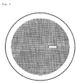
- Lattice grooves having a rectangular sectional form having a width of 1.0 mm, a depth of 0.5 mm and a pitch of 20 mm were formed in an area (excluding a portion corresponding to the light transmitting area) having a radius of 250 mm from the center of the pad of the non-polishing side of the molded product.
- Fig. 3 is a schematic diagram of the recessed portions formed on the non-polishing side.
- the double-coated adhesive tape on the non-polishing side (rear surface) of the IC1000 chemical mechanical polishing pad (consisting of a single layer) of Rohm and Haas Electronics, Materials Co., Ltd. was removed and concentric grooves (having a rectangular sectional form) having a width of 1.0 mm, a pitch of 2.0 mm and a depth of 0. 5 mm were formed on the non-polishing side (rear surface) by a commercially available cutting machine. Thereafter, a double-coated adhesive tape having the same plane shape as the pad was affixed to the non-polishing side.
- the chemical mechanical polishing performance was evaluated in the same manner as in Example 1 except that the thus manufactured chemical mechanical polishing pad was used. Since the obtained chemical mechanical polishing pad had no light transmitting portion for transmitting detection light from the optical end-point detector, the first-stage polishing in (2-3) polishing of a wafer having the pattern of copper and low-dielectric insulating films was carried out for 120 seconds without using the optical end-point detector.
- a disk-like molded product was obtained by carrying in the same manners as in (1-1) preparation of composition for chemical mechanical polishing pads and (1-2) formation of rough shape of pad of Example 1.
- concentric grooves having a rectangular sectional form
- concentric grooves having a width of 0.5 mm, a pitch of 2.0 mm and a depth of 1.0 mm were formed on the polishing side of the above molded product by a commercially available cutting machine.
- a double-coated adhesive tape having the same plane shape as the pad was affixed to the non-polishing side and a portion covering the thin portion for end-point detection (light transmitting area) of the double-coated adhesive tape was cut away to manufacture a chemical mechanical polishing pad having no recessed portion on the non-polishing side.
- a disk-like molded product was obtained by carrying in the same manners as in (1-1) preparation of composition for chemical mechanical polishing pads and (1-2) formation of rough shape of pad of Example 1.
- concentric grooves having a rectangular sectional form
- Lattice grooves having a rectangular sectional form
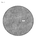
- Lattice grooves having a width of 1.0 mm, a depth of 0.5 mm and a pitch of 20 mm were formed on the entire non-polishing side (excluding a portion corresponding to a light transmitting area) of this molded product.
- the formed lattice grooves reached the end of the pad.
- a double-coated adhesive tape having the same plane shape as the pad was affixed to the non-polishing side and a portion covering the thin portion for end-point detection (light transmitting area) of the double-coated adhesive tape was cut away.
- Fig. 4 is a schematic diagram of the recessed portions formed on the non-polishing side.
- the chemical mechanical polishing performance was evaluated in the same manner as in Example 1 except that the IC1000 chemical mechanical polishing pad of Rohm and Haas Electronic Materials Co. , Ltd. (consisting of a single layer) was used. Since this chemical mechanical polishing pad had no light transmitting portion for transmitting detection light from the optical end-point detector, the first-stage polishing in (2-3) polishing of a wafer having the pattern of copper and a low-dielectric insulating films was carried out for 120 seconds without using the optical end-point detector. The results are shown in Table 1.
Landscapes
- Engineering & Computer Science (AREA)
- Mechanical Engineering (AREA)
- Chemical & Material Sciences (AREA)
- Materials Engineering (AREA)
- Organic Chemistry (AREA)
- Mechanical Treatment Of Semiconductor (AREA)
- Finish Polishing, Edge Sharpening, And Grinding By Specific Grinding Devices (AREA)
- Polishing Bodies And Polishing Tools (AREA)
Claims (6)
- Chemisch, mechanisches Polierkissen, das eine Fläche zum Polieren eines zu polierenden Objekts, eine Nicht-Polierfläche gegenüber zu der Fläche und eine Seitenfläche zum Verbinden dieser Flächen miteinander aufweist, und ein Muster von Vertiefungsabschnitten beinhaltet, welche an der Nicht-Polierfläche gebildet sind, dadurch gekennzeichnet, dass die Vertiefungsabschnitte zu der Nicht-Polierfläche und nicht zu der Seitenfläche offen sind.
- Chemisch, mechanisches Polierkissen nach Anspruch 1, wobei die Vertiefungsabschnitte, die das Muster an der Nicht-Polierfläche bilden, kreisförmig, elliptisch, polygonal oder nutartig sind.
- Chemisch, mechanisches Polierkissen nach Anspruch 1, welches ferner einen kreisförmigen oder polygonalen Vertiefungsabschnitt aufweist, welcher nicht das Muster in dem Zentralabschnitt der Nicht-Polierfläche bildet.
- Chemisch, mechanisches Polierkissen nach Anspruch 1, welches ferner einen Bereich mit hohen Lichttransmissionseigenschaften in einem anderen Abschnitt als dem Zentralabschnitt der Nicht-Polierfläche aufweist.
- Chemisch, mechanisches Polierkissen nach Anspruch 4, wobei der Bereich mit hohen Lichttransmissionseigenschaften ein Vertiefungsabschnitt ist, der in einem anderen Abschnitt als dem Zentralabschnitt der Nicht-Polierfläche gebildet ist.
- Chemisch, mechanisches Polierkissen nach Anspruch 1, welches ein wasserunlösliches Material und in dem wasserunlöslichen Material dispergierte wasserlösliche Teilchen umfasst.
Applications Claiming Priority (2)
| Application Number | Priority Date | Filing Date | Title |
|---|---|---|---|
| JP2003374855 | 2003-11-04 | ||
| JP2003374855 | 2003-11-04 |
Publications (2)
| Publication Number | Publication Date |
|---|---|
| EP1529598A1 EP1529598A1 (de) | 2005-05-11 |
| EP1529598B1 true EP1529598B1 (de) | 2009-07-29 |
Family
ID=34431266
Family Applications (1)
| Application Number | Title | Priority Date | Filing Date |
|---|---|---|---|
| EP04026070A Expired - Lifetime EP1529598B1 (de) | 2003-11-04 | 2004-11-03 | Chemisch-mechanische Polierscheibe |
Country Status (6)
| Country | Link |
|---|---|
| US (1) | US7442116B2 (de) |
| EP (1) | EP1529598B1 (de) |
| KR (1) | KR101314013B1 (de) |
| CN (1) | CN100437924C (de) |
| DE (1) | DE602004022237D1 (de) |
| TW (1) | TWI337110B (de) |
Families Citing this family (19)
| Publication number | Priority date | Publication date | Assignee | Title |
|---|---|---|---|---|
| USD559063S1 (en) * | 2004-03-17 | 2008-01-08 | Jsr Corporation | Polishing pad |
| USD559064S1 (en) | 2004-03-17 | 2008-01-08 | Jsr Corporation | Polishing pad |
| USD559648S1 (en) * | 2004-10-05 | 2008-01-15 | Jsr Corporation | Polishing pad |
| TWD111897S1 (zh) * | 2004-10-05 | 2006-07-11 | 股份有限公司 | 研磨用墊片 |
| USD560457S1 (en) * | 2004-10-05 | 2008-01-29 | Jsr Corporation | Polishing pad |
| USD559066S1 (en) | 2004-10-26 | 2008-01-08 | Jsr Corporation | Polishing pad |
| JP3872081B2 (ja) * | 2004-12-29 | 2007-01-24 | 東邦エンジニアリング株式会社 | 研磨用パッド |
| US20070149094A1 (en) * | 2005-12-28 | 2007-06-28 | Choi Jae Y | Monitoring Device of Chemical Mechanical Polishing Apparatus |
| TWI411495B (zh) * | 2007-08-16 | 2013-10-11 | Cabot Microelectronics Corp | 拋光墊 |
| KR20100096459A (ko) * | 2009-02-24 | 2010-09-02 | 삼성전자주식회사 | 화학적 기계적 연마장치 |
| BR112013014711A2 (pt) * | 2010-12-16 | 2016-10-04 | 3M Innovative Properties Co | blocos compósitos com espaços livres |
| US9211628B2 (en) * | 2011-01-26 | 2015-12-15 | Nexplanar Corporation | Polishing pad with concentric or approximately concentric polygon groove pattern |
| CN102284916A (zh) * | 2011-07-04 | 2011-12-21 | 南京航空航天大学 | 具有复合排屑结构的研磨抛光垫 |
| CN102744676A (zh) * | 2012-07-26 | 2012-10-24 | 上海宏力半导体制造有限公司 | 用于化学机械研磨的研磨垫以及化学机械研磨设备 |
| US9259818B2 (en) * | 2012-11-06 | 2016-02-16 | Sinmat, Inc. | Smooth diamond surfaces and CMP method for forming |
| DE102015106441B4 (de) * | 2015-04-27 | 2022-01-27 | Infineon Technologies Ag | Verfahren zum Planarisieren eines Halbleiterwafers |
| JP7113626B2 (ja) * | 2018-01-12 | 2022-08-05 | ニッタ・デュポン株式会社 | 研磨パッド |
| USD982257S1 (en) * | 2021-01-20 | 2023-03-28 | The Vetreska Pet Lifestyle Company | Cat tree |
| USD982256S1 (en) * | 2021-01-20 | 2023-03-28 | The Vetreska Pet Lifestyle Company | Cat tree |
Family Cites Families (19)
| Publication number | Priority date | Publication date | Assignee | Title |
|---|---|---|---|---|
| MY114512A (en) | 1992-08-19 | 2002-11-30 | Rodel Inc | Polymeric substrate with polymeric microelements |
| US5650039A (en) | 1994-03-02 | 1997-07-22 | Applied Materials, Inc. | Chemical mechanical polishing apparatus with improved slurry distribution |
| JPH08216029A (ja) | 1995-02-07 | 1996-08-27 | Daiki:Kk | 精密研磨シート |
| US5921855A (en) | 1997-05-15 | 1999-07-13 | Applied Materials, Inc. | Polishing pad having a grooved pattern for use in a chemical mechanical polishing system |
| JP3668046B2 (ja) | 1998-05-11 | 2005-07-06 | 株式会社東芝 | 研磨布及びこの研磨布を用いた半導体装置の製造方法 |
| JP3918359B2 (ja) | 1998-05-15 | 2007-05-23 | Jsr株式会社 | 研磨パッド用重合体組成物および研磨パッド |
| US6221298B1 (en) * | 1998-11-17 | 2001-04-24 | International Specialty Products, Llc | Method and apparatus for manufacturing molded products |
| US6217426B1 (en) | 1999-04-06 | 2001-04-17 | Applied Materials, Inc. | CMP polishing pad |
| US6171181B1 (en) * | 1999-08-17 | 2001-01-09 | Rodel Holdings, Inc. | Molded polishing pad having integral window |
| US6699104B1 (en) * | 1999-09-15 | 2004-03-02 | Rodel Holdings, Inc. | Elimination of trapped air under polishing pads |
| KR100336764B1 (ko) * | 1999-10-20 | 2002-05-16 | 박종섭 | 화학 기계적 연마용 패드의 구조 |
| JP3925041B2 (ja) | 2000-05-31 | 2007-06-06 | Jsr株式会社 | 研磨パッド用組成物及びこれを用いた研磨パッド |
| US6656019B1 (en) * | 2000-06-29 | 2003-12-02 | International Business Machines Corporation | Grooved polishing pads and methods of use |
| JP4686010B2 (ja) | 2000-07-18 | 2011-05-18 | ニッタ・ハース株式会社 | 研磨パッド |
| KR100641086B1 (ko) * | 2001-02-08 | 2006-11-06 | 주식회사 하이닉스반도체 | 반도체소자의 화학기계적연마에 의한 스크래치 방지방법 |
| KR100858392B1 (ko) * | 2001-04-25 | 2008-09-11 | 제이에스알 가부시끼가이샤 | 반도체 웨이퍼용 연마 패드와, 이를 구비한 반도체웨이퍼용 연마 적층체와, 반도체 웨이퍼의 연마 방법 |
| US20040259479A1 (en) * | 2003-06-23 | 2004-12-23 | Cabot Microelectronics Corporation | Polishing pad for electrochemical-mechanical polishing |
| US6942549B2 (en) * | 2003-10-29 | 2005-09-13 | International Business Machines Corporation | Two-sided chemical mechanical polishing pad for semiconductor processing |
| US20090053983A1 (en) * | 2006-01-25 | 2009-02-26 | Jsr Corporation | Chemical mechanical polishing pad and method for manufacturing same |
-
2004
- 2004-11-02 US US10/978,472 patent/US7442116B2/en not_active Expired - Fee Related
- 2004-11-03 DE DE602004022237T patent/DE602004022237D1/de not_active Expired - Lifetime
- 2004-11-03 EP EP04026070A patent/EP1529598B1/de not_active Expired - Lifetime
- 2004-11-04 TW TW093133682A patent/TWI337110B/zh not_active IP Right Cessation
- 2004-11-04 KR KR1020040089199A patent/KR101314013B1/ko not_active Expired - Fee Related
- 2004-11-04 CN CNB2004100903620A patent/CN100437924C/zh not_active Expired - Fee Related
Also Published As
| Publication number | Publication date |
|---|---|
| CN1614749A (zh) | 2005-05-11 |
| US7442116B2 (en) | 2008-10-28 |
| CN100437924C (zh) | 2008-11-26 |
| KR101314013B1 (ko) | 2013-10-01 |
| EP1529598A1 (de) | 2005-05-11 |
| KR20050042738A (ko) | 2005-05-10 |
| US20050113011A1 (en) | 2005-05-26 |
| TW200531784A (en) | 2005-10-01 |
| DE602004022237D1 (de) | 2009-09-10 |
| TWI337110B (en) | 2011-02-11 |
Similar Documents
| Publication | Publication Date | Title |
|---|---|---|
| EP1529598B1 (de) | Chemisch-mechanische Polierscheibe | |
| KR100669301B1 (ko) | 연마 패드 및 복층형 연마 패드 | |
| KR100858392B1 (ko) | 반도체 웨이퍼용 연마 패드와, 이를 구비한 반도체웨이퍼용 연마 적층체와, 반도체 웨이퍼의 연마 방법 | |
| EP1739729B1 (de) | Polierstück für einen halbleiterwafer, polier-mehrschichtkörper für einen halbleiterwafer damit und verfahren zum polieren eines halbleiterwafers | |
| EP1498222B1 (de) | Chemisch-mechanisches Polierkissen und Polierverfahren | |
| US20040203320A1 (en) | Abrasive pad, method and metal mold for manufacturing the same, and semiconductor wafer polishing method | |
| EP1591201B1 (de) | Kissen zum chemisch-mechanischen Polieren, Herstellungsverfahren dafür und chemisch-mechanisches Polierverfahren für Halbleiterwafer | |
| US20050239380A1 (en) | Chemical mechanical polishing pad, manufacturing process thereof and chemical mechanical polishing method | |
| US7097550B2 (en) | Chemical mechanical polishing pad | |
| JP3826729B2 (ja) | 半導体ウエハ用研磨パッド及びこれを備える半導体ウエハ用研磨複層体並びに半導体ウエハの研磨方法 | |
| JP2002324769A (ja) | 半導体ウエハ用研磨パッド及びこれを備える半導体ウエハ用研磨複層体並びに半導体ウエハの研磨方法 | |
| EP1479479B1 (de) | Polierkissen | |
| JP3849582B2 (ja) | 研磨パッド及び複層型研磨パッド | |
| JP3849593B2 (ja) | 研磨パッド及び複層型研磨パッド | |
| JP3849594B2 (ja) | 研磨パッド | |
| JP4877448B2 (ja) | 化学機械研磨パッド | |
| JP2004134539A (ja) | 半導体ウエハ用研磨パッド及びこれを備える半導体ウエハ用研磨複層体並びに半導体ウエハの研磨方法 | |
| JP2004146704A (ja) | 半導体ウェハ用研磨パッドの加工方法及び半導体ウェハ用研磨パッド | |
| JP3867629B2 (ja) | 研磨パッド及び複層型研磨パッド | |
| KR100710788B1 (ko) | 반도체 웨이퍼용 연마 패드 및 이것을 구비하는 반도체웨이퍼용 연마 복층체 및 반도체 웨이퍼의 연마 방법 |
Legal Events
| Date | Code | Title | Description |
|---|---|---|---|
| PUAI | Public reference made under article 153(3) epc to a published international application that has entered the european phase |
Free format text: ORIGINAL CODE: 0009012 |
|
| AK | Designated contracting states |
Kind code of ref document: A1 Designated state(s): AT BE BG CH CY CZ DE DK EE ES FI FR GB GR HU IE IS IT LI LU MC NL PL PT RO SE SI SK TR |
|
| AX | Request for extension of the european patent |
Extension state: AL HR LT LV MK YU |
|
| 17P | Request for examination filed |
Effective date: 20050922 |
|
| AKX | Designation fees paid |
Designated state(s): DE FR IT |
|
| GRAP | Despatch of communication of intention to grant a patent |
Free format text: ORIGINAL CODE: EPIDOSNIGR1 |
|
| GRAS | Grant fee paid |
Free format text: ORIGINAL CODE: EPIDOSNIGR3 |
|
| GRAA | (expected) grant |
Free format text: ORIGINAL CODE: 0009210 |
|
| AK | Designated contracting states |
Kind code of ref document: B1 Designated state(s): DE FR IT |
|
| REF | Corresponds to: |
Ref document number: 602004022237 Country of ref document: DE Date of ref document: 20090910 Kind code of ref document: P |
|
| PLBE | No opposition filed within time limit |
Free format text: ORIGINAL CODE: 0009261 |
|
| STAA | Information on the status of an ep patent application or granted ep patent |
Free format text: STATUS: NO OPPOSITION FILED WITHIN TIME LIMIT |
|
| 26N | No opposition filed |
Effective date: 20100503 |
|
| REG | Reference to a national code |
Ref country code: FR Ref legal event code: PLFP Year of fee payment: 12 |
|
| REG | Reference to a national code |
Ref country code: FR Ref legal event code: PLFP Year of fee payment: 13 |
|
| REG | Reference to a national code |
Ref country code: FR Ref legal event code: PLFP Year of fee payment: 14 |
|
| PGFP | Annual fee paid to national office [announced via postgrant information from national office to epo] |
Ref country code: DE Payment date: 20191121 Year of fee payment: 16 |
|
| PGFP | Annual fee paid to national office [announced via postgrant information from national office to epo] |
Ref country code: FR Payment date: 20191120 Year of fee payment: 16 Ref country code: IT Payment date: 20191128 Year of fee payment: 16 |
|
| REG | Reference to a national code |
Ref country code: DE Ref legal event code: R119 Ref document number: 602004022237 Country of ref document: DE |
|
| PG25 | Lapsed in a contracting state [announced via postgrant information from national office to epo] |
Ref country code: FR Free format text: LAPSE BECAUSE OF NON-PAYMENT OF DUE FEES Effective date: 20201130 Ref country code: IT Free format text: LAPSE BECAUSE OF NON-PAYMENT OF DUE FEES Effective date: 20201103 |
|
| PG25 | Lapsed in a contracting state [announced via postgrant information from national office to epo] |
Ref country code: DE Free format text: LAPSE BECAUSE OF NON-PAYMENT OF DUE FEES Effective date: 20210601 |