EP1528847A1 - Wärmeableiteinsatz, Schaltung mit einem solchen Einsatz und Verfahren zur Herstellung - Google Patents
Wärmeableiteinsatz, Schaltung mit einem solchen Einsatz und Verfahren zur Herstellung Download PDFInfo
- Publication number
- EP1528847A1 EP1528847A1 EP03425697A EP03425697A EP1528847A1 EP 1528847 A1 EP1528847 A1 EP 1528847A1 EP 03425697 A EP03425697 A EP 03425697A EP 03425697 A EP03425697 A EP 03425697A EP 1528847 A1 EP1528847 A1 EP 1528847A1
- Authority
- EP
- European Patent Office
- Prior art keywords
- dissipative
- insert
- circuit
- board
- electronic
- Prior art date
- Legal status (The legal status is an assumption and is not a legal conclusion. Google has not performed a legal analysis and makes no representation as to the accuracy of the status listed.)
- Granted
Links
Images

Classifications
-
- H—ELECTRICITY
- H05—ELECTRIC TECHNIQUES NOT OTHERWISE PROVIDED FOR
- H05K—PRINTED CIRCUITS; CASINGS OR CONSTRUCTIONAL DETAILS OF ELECTRIC APPARATUS; MANUFACTURE OF ASSEMBLAGES OF ELECTRICAL COMPONENTS
- H05K7/00—Constructional details common to different types of electric apparatus
- H05K7/20—Modifications to facilitate cooling, ventilating, or heating
- H05K7/2039—Modifications to facilitate cooling, ventilating, or heating characterised by the heat transfer by conduction from the heat generating element to a dissipating body
- H05K7/20436—Inner thermal coupling elements in heat dissipating housings, e.g. protrusions or depressions integrally formed in the housing
- H05K7/20445—Inner thermal coupling elements in heat dissipating housings, e.g. protrusions or depressions integrally formed in the housing the coupling element being an additional piece, e.g. thermal standoff
-
- H—ELECTRICITY
- H05—ELECTRIC TECHNIQUES NOT OTHERWISE PROVIDED FOR
- H05K—PRINTED CIRCUITS; CASINGS OR CONSTRUCTIONAL DETAILS OF ELECTRIC APPARATUS; MANUFACTURE OF ASSEMBLAGES OF ELECTRICAL COMPONENTS
- H05K1/00—Printed circuits
- H05K1/02—Details
- H05K1/0201—Thermal arrangements, e.g. for cooling, heating or preventing overheating
- H05K1/0203—Cooling of mounted components
- H05K1/0204—Cooling of mounted components using means for thermal conduction connection in the thickness direction of the substrate
-
- H—ELECTRICITY
- H10—SEMICONDUCTOR DEVICES; ELECTRIC SOLID-STATE DEVICES NOT OTHERWISE PROVIDED FOR
- H10W—GENERIC PACKAGES, INTERCONNECTIONS, CONNECTORS OR OTHER CONSTRUCTIONAL DETAILS OF DEVICES COVERED BY CLASS H10
- H10W40/00—Arrangements for thermal protection or thermal control
- H10W40/20—Arrangements for cooling
- H10W40/22—Arrangements for cooling characterised by their shape, e.g. having conical or cylindrical projections
- H10W40/226—Arrangements for cooling characterised by their shape, e.g. having conical or cylindrical projections characterised by projecting parts, e.g. fins to increase surface area
- H10W40/228—Arrangements for cooling characterised by their shape, e.g. having conical or cylindrical projections characterised by projecting parts, e.g. fins to increase surface area the projecting parts being wire-shaped or pin-shaped
-
- H—ELECTRICITY
- H05—ELECTRIC TECHNIQUES NOT OTHERWISE PROVIDED FOR
- H05K—PRINTED CIRCUITS; CASINGS OR CONSTRUCTIONAL DETAILS OF ELECTRIC APPARATUS; MANUFACTURE OF ASSEMBLAGES OF ELECTRICAL COMPONENTS
- H05K2201/00—Indexing scheme relating to printed circuits covered by H05K1/00
- H05K2201/10—Details of components or other objects attached to or integrated in a printed circuit board
- H05K2201/10007—Types of components
- H05K2201/10166—Transistor
-
- H—ELECTRICITY
- H05—ELECTRIC TECHNIQUES NOT OTHERWISE PROVIDED FOR
- H05K—PRINTED CIRCUITS; CASINGS OR CONSTRUCTIONAL DETAILS OF ELECTRIC APPARATUS; MANUFACTURE OF ASSEMBLAGES OF ELECTRICAL COMPONENTS
- H05K2201/00—Indexing scheme relating to printed circuits covered by H05K1/00
- H05K2201/10—Details of components or other objects attached to or integrated in a printed circuit board
- H05K2201/10227—Other objects, e.g. metallic pieces
- H05K2201/10416—Metallic blocks or heatsinks completely inserted in a PCB
Definitions
- the present invention relates to an electronic circuit comprising a board with printed circuits and means for heat dissipation for its electronic components such as the power components, for example diodes and MOSFETs.
- power components that require measures for heat dissipation are mounted include elements in thermal contact with these power components having the function of conducting heat from inside the chip, where this heat develops, to an external device that facilitates dissipation.
- the electronic power component is fixed to an element of the heat dissipator using suitable fixing means, such as elastic springs or thermally conductive adhesives.
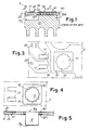
- the electronic circuit in Figure 1 describes an exemplifying embodiment of the state of the art comprising an electronic board 1 with printed circuits - not shown in the Figure - on two upper and lower surfaces, 21 and 22 respectively, and a heat dissipation system for an electronic power component 5 fixed to the electronic board 1.
- the power component 5 is placed on an insulator 3 forming the support of the electronic board 1, so that the conductive pins 33 of the component 5 are soldered to respective contacts 17 of the printed circuit produced on the upper face 21 of the insulating support 3, and the area corresponding to the joint 5G of the component 5 is glued to a conductive pad 15' of this printed circuit.
- a conductive adhesive used to form a layer 31 and metallized through-holes 5F that connect the pad 15' with a pad 15" of a printed circuit produced on the lower face 22 of the insulating support 3.
- This pad 15" comes into contact with a raised part 13R of a dissipator 13, to form the thermal connection between the power component and said dissipator.
- This raised part 13R of the dissipator 13 is necessary as it performs the function of moving the lower surface 13S of the dissipator away from contacts and solderings for electronic components produced on this face 22 of the insulating support 3.
- the invention relates to an electronic circuit that comprises a board with printed circuits and heat dissipation systems for electronic power components mounted thereon to improve thermal contact and heat conduction from these electronic components to a dissipation device, which overcomes the drawbacks of prior art dissipation systems.
- heat conduction is guaranteed by a conductive dissipative insert inserted inside a through-hole produced in the insulating layer of the electronic board at the level of the pad on which the power component is mounted.
- This dissipative insert advantageously has flat and continuous heat exchange faces, a first of which in contact with the electronic power component and a second in contact with the heat dissipater; in this way the heat exchange surface increases with consequent improvement in the conduction of heat between power component and dissipator.
- the first face of the insert is preferably flush with the surface of the electronic board on which the power component is mounted, the second face projects advantageously from the opposed surface of said board for a length that guarantees the distance of the dissipator from the surface of the board on which the contact solderings of the components and/or further electronic components are produced.
- An electronic circuit that comprises boards with printed circuits according to the invention is therefore generally composed of a plurality of electronic components, some of which power components, and of a plurality of corresponding dissipative inserts.
- This plurality of dissipative inserts is advantageously characterized in that it projects by the same amount from the second surface of the electronic board, so that the respective second faces of the various inserts are aligned on the same plane.
- dissipators As electronic boards generally have standard dimensions, with the principle underlying the invention it is possible to produce a limited number of dissipators, for example equal to the number of boards of different dimensions employed. According to the layout of the individual electronic circuit, heat dissipation of the various power components is guaranteed by suitable distribution of the dissipative inserts at the level of the positions of the power components. A single dimension or a limited number of dimensions of the dissipative inserts may be used for power components that differ even greatly in forms and dimensions.
- the dissipative insert is produced in a conductive material, such as copper, in order to connect the electronic component both thermally to the dissipator, and if necessary electrically to the pad of a printed circuit on the second surface of the board.
- the insert may also be coated with a material that is easy to solder to the electronic circuit, such as nickel or tin, to facilitate soldering.
- a material that is easy to solder to the electronic circuit such as nickel or tin, to facilitate soldering.
- electrically insulating elements which are excellent heat conductors are provided on the face of the insert in contact with the heat dissipator, for example gap fillers, i.e. thin silicone rubber pads enriched with heat conducting materials, to obtain thermal conduction electrically insulating the dissipator.
- an electronic circuit comprises boards with printed circuits with several layers produced inside the insulating support and dissipative inserts that electrically connect the respective electronic power components with at least one of these printed circuit layers.
- the heat dissipator is produced by the external container of said electronic board.
- the dissipative inserts may be in direct thermal contact (or with the interposition of thermally conductive electric insulators) with the housing of the electronic circuit.
- the dissipative insert in the preferred embodiment has a cylindrical form with a circular section, or if needed a slightly conical form to facilitate insertion into the hole. It may be provided with apertures, for examples cuts or slots, to increase deformability and/or facilitate insertion, or to increase the heat exchange surface with the environment and be used directly as a heat dissipator, without being connected to an additional dissipation element. In the preferred embodiment, however, the dissipative insert will have a simple geometric form, especially a cylindrical form, to reduce production costs.
- Electronic components may also be fixed to flat walls orthogonal to the electronic board applied to the dissipative inserts according to the invention, by means of traditional fixing systems such as elastic springs, or using a mounting system for horizontally positioned components.
- the dissipative inserts may therefore be in the form of a parallelepiped with a polygonal section, preferably square or rectangular, on at least one face of which a power component is advantageously fixed.
- this dissipative insert is soldered in the through-hole, although other methods may be used to fix it to the electronic board, such as coupling with interference, obtained by deforming the edge of the hole and/or the dissipative insert.
- the edge of the hole may advantageously include means, such as undulations or serrations, to facilitate not only insertion of the insert, but also thermal contact and the actual soldering process, allowing the solder material to penetrate between the surface of the hole and the lateral surface of the dissipative insert. Among other things, this avoids the risk of the power component tending to "float" on the molten solder paste during the soldering phase.
- the invention also relates to a method to produce an electronic circuit comprising at least a power component and a corresponding dissipative insert.
- a through-hole if necessary with a serrated edge, is first produced on an electronic board, at the level of the pad of an electronic power component; the dissipative insert is then inserted so that a first of its faces is advantageously flush with the surface of the electronic board on which the single power component is mounted, while the second face projects from the opposed surface of the electronic board. Subsequently the power component is applied, in thermal contact with the dissipative insert.
- a solder paste is applied to the pad and to the first face of the insert - by silk-screening or any other known method.
- the power component is subsequently placed on the solder paste and its contact pins are positioned on the specific contacts of the electronic board to which the solder paste was applied with the same silk-screening or other known system.
- the operation described above is in practice performed for all the power components of the circuit.
- the board is placed in the oven for reflow soldering. Heating causes the solder paste to melt.
- the serrations on the edge of the hole allow increased infiltration of the solder paste on the contact surfaces between the hole and the insert.
- a heat dissipator with a flat face in thermal contact with the second face of each dissipative insert is fixed to the board, electrically insulating said dissipator by applying electric insulating means and heat conductors to the areas of thermal contact.
- Mounting of the dissipative inserts and of the various power and logic components may be performed using SMD technology.
- the various components may also be soldered with other known systems.
- an electronic circuit comprises a board with printed circuits according to the present invention indicated generically with 10, see Figure 2.
- the electronic board 10 is constituted by an electrically insulated support 3, on the upper surface 21 of which conductive tracks 18 are produced, see Figure 3, forming a printed circuit, that electrically connect a plurality of electronic logic components 7 and electronic power components 5.
- the printed circuit with the conductive tracks 18 is produced in a way per se known and not described herein.
- the components herein denominated “logic components” are all those components that do not require thermal contact with a heat dissipator.
- the components herein denominated “power components” are in general those that require thermal contact with a heat dissipator, that is with a heat sink.
- the electronic power components 5 are in contact with dissipative inserts 9 inserted in through-holes 11 produced in the electronic board 10.
- These dissipative inserts 9 are, moreover, in contact with a heat dissipator 13 at a distance from the opposed surface 23 of the electronic board 10.
- the through-holes 11 are advantageously provided with serrations 16, see Figure 3, and produced in the conductive pad 15' of the printed circuit on which a power component 5 is positioned. Electric contacts 17 of the printed circuit 18 for pins 33 of a power component 5 are produced at a distance from the pad 15'.
- Figure 4 shows a dissipative insert 9 with a circular section inserted in the through-hole 11 in Figure 3.
- the external surface of said insert 9 defines with the serrations 16 a series of through apertures 19 suitable to improve insertion of the insert and drainage of the solder paste from the upper face 21 to the lower face 22 during soldering.
- Figure 5 shows a vertical section of the area of the circuit according to the embodiment described comprising: on the face 21 of the insulating support 3 the conducting pad 15 for subsequent positioning of the power component 5, the contacts 17 for the pins of the component 5 and a conducting pad 15" of a printed circuit - not shown in the Figures - on the lower face 22.
- a solder paste is applied (with a silkscreen procedure or any another suitable way) to the upper surface 9A of the insert and on the pad 15'.
- This operation is performed for all the inserts 9 inserted in the board and analogously the solder paste is also applied on the connecting pads 17 for the pins of the power component, and on other pads of the electronic board on which the other electronic components are to be soldered. Subsequently, with an SMD mounting technique or in another suitable way, the various electronic logic (7) and power (5) components are applied to the board.
- Figure 6 shows a section of a detail of the area of the circuit relative to the invention: the electronic power component 5 is positioned on a layer 31 of solder paste applied to the conducting pad 15' produced as in Figure 5.
- the solder paste has also been applied in 35 and 37 to solder the leads 33 and 39 of the power component 5 to the contacts 17 and the conducting pad 15' respectively.
- solder paste is then melted by placing the circuit in the oven.
- the solder paste applied to the dissipative insert 9 melts to penetrate through the apertures 19 ( Figure 4) and reaches the face of the board opposed to the one on which the component 5 is applied, forming a solder area 40.
- an electrically insulating and thermally conductive layer 41 is interposed, to electrically insulate the electronic components in respect of the dissipator 13 and allow heat conduction between these components and said dissipator 13.
- the dissipator 13 has a flat contact surface with all the dissipative inserts 9 in the electronic circuit, as can be seen in particular in Figure 2. It may thereby be produced with noteworthy savings on costs in respect of the dissipator 13 in Figure 1. Moreover, it is unnecessary to provide different dissipators, dedicated to the single circuits.
- the circuit may also be placed directly in thermal contact, by means of the surfaces 9B of the inserts 9, with a thermally conductive container wherein the circuit is housed. Also in this case electrically insulating and thermally conductive layers or strips may be provided between the surfaces 9A of the inserts 9 and the surface of the container with which said inserts are brought into thermal contact.
Landscapes
- Engineering & Computer Science (AREA)
- Microelectronics & Electronic Packaging (AREA)
- Physics & Mathematics (AREA)
- Thermal Sciences (AREA)
- Cooling Or The Like Of Electrical Apparatus (AREA)
- Structure Of Printed Boards (AREA)
- Encapsulation Of And Coatings For Semiconductor Or Solid State Devices (AREA)
Priority Applications (3)
| Application Number | Priority Date | Filing Date | Title |
|---|---|---|---|
| DE60315469T DE60315469T2 (de) | 2003-10-29 | 2003-10-29 | Wärmeableiteinsatz, Schaltung mit einem solchen Einsatz und Verfahren zur Herstellung |
| EP03425697A EP1528847B1 (de) | 2003-10-29 | 2003-10-29 | Wärmeableiteinsatz, Schaltung mit einem solchen Einsatz und Verfahren zur Herstellung |
| AT03425697T ATE369724T1 (de) | 2003-10-29 | 2003-10-29 | Wärmeableiteinsatz, schaltung mit einem solchen einsatz und verfahren zur herstellung |
Applications Claiming Priority (1)
| Application Number | Priority Date | Filing Date | Title |
|---|---|---|---|
| EP03425697A EP1528847B1 (de) | 2003-10-29 | 2003-10-29 | Wärmeableiteinsatz, Schaltung mit einem solchen Einsatz und Verfahren zur Herstellung |
Publications (2)
| Publication Number | Publication Date |
|---|---|
| EP1528847A1 true EP1528847A1 (de) | 2005-05-04 |
| EP1528847B1 EP1528847B1 (de) | 2007-08-08 |
Family
ID=34400633
Family Applications (1)
| Application Number | Title | Priority Date | Filing Date |
|---|---|---|---|
| EP03425697A Expired - Lifetime EP1528847B1 (de) | 2003-10-29 | 2003-10-29 | Wärmeableiteinsatz, Schaltung mit einem solchen Einsatz und Verfahren zur Herstellung |
Country Status (3)
| Country | Link |
|---|---|
| EP (1) | EP1528847B1 (de) |
| AT (1) | ATE369724T1 (de) |
| DE (1) | DE60315469T2 (de) |
Cited By (7)
| Publication number | Priority date | Publication date | Assignee | Title |
|---|---|---|---|---|
| WO2006109206A3 (en) * | 2005-04-12 | 2007-04-26 | Koninkl Philips Electronics Nv | Electronic circuit module comprising a heat producing component |
| DE102007037297A1 (de) * | 2007-08-07 | 2009-02-19 | Continental Automotive Gmbh | Schaltungsträgeraufbau mit verbesserter Wärmeableitung |
| CN102014600A (zh) * | 2010-12-21 | 2011-04-13 | 摩比天线技术(深圳)有限公司 | 一种散热结构及其制作方法、具有散热结构的电子设备 |
| FR2999863A1 (fr) * | 2012-12-14 | 2014-06-20 | Valeo Systemes Thermiques | Circuit imprime comportant un insert caloporteur |
| KR20170118599A (ko) * | 2016-04-15 | 2017-10-25 | 오므론 가부시키가이샤 | 반도체 장치의 방열구조 |
| CN108200719A (zh) * | 2018-02-28 | 2018-06-22 | 浙江联宜电机有限公司 | 驱动器功率器件散热结构 |
| WO2021252933A3 (en) * | 2020-06-12 | 2022-02-17 | Raytheon Company | Shape memory thermal capacitor and methods for same |
Families Citing this family (3)
| Publication number | Priority date | Publication date | Assignee | Title |
|---|---|---|---|---|
| JP5861846B2 (ja) * | 2011-11-02 | 2016-02-16 | 富士電機株式会社 | 電力変換器およびその製造方法 |
| DE102018215338B3 (de) | 2018-09-10 | 2020-01-16 | Dürkopp Adler AG | Kühlvorrichtung für mindestens ein auf einer Leiterplatte montiertes Bauelement |
| DE102019129586A1 (de) * | 2019-11-04 | 2021-05-06 | Hanon Systems | Verbindungselement zum Verbinden einer Leiterplatte mit einem Kühlkörper und Verfahren zur Herstellung der Verbindung |
Citations (3)
| Publication number | Priority date | Publication date | Assignee | Title |
|---|---|---|---|---|
| US5014904A (en) * | 1990-01-16 | 1991-05-14 | Cray Research, Inc. | Board-mounted thermal path connector and cold plate |
| EP0741504A2 (de) * | 1995-05-05 | 1996-11-06 | Robert Bosch Gmbh | Metallleiterplatte und Verfahren zur Herstellung |
| DE20301773U1 (de) * | 2003-02-05 | 2003-04-17 | Leopold Kostal GmbH & Co. KG, 58507 Lüdenscheid | Elektrische Einrichtung |
-
2003
- 2003-10-29 DE DE60315469T patent/DE60315469T2/de not_active Expired - Fee Related
- 2003-10-29 EP EP03425697A patent/EP1528847B1/de not_active Expired - Lifetime
- 2003-10-29 AT AT03425697T patent/ATE369724T1/de not_active IP Right Cessation
Patent Citations (3)
| Publication number | Priority date | Publication date | Assignee | Title |
|---|---|---|---|---|
| US5014904A (en) * | 1990-01-16 | 1991-05-14 | Cray Research, Inc. | Board-mounted thermal path connector and cold plate |
| EP0741504A2 (de) * | 1995-05-05 | 1996-11-06 | Robert Bosch Gmbh | Metallleiterplatte und Verfahren zur Herstellung |
| DE20301773U1 (de) * | 2003-02-05 | 2003-04-17 | Leopold Kostal GmbH & Co. KG, 58507 Lüdenscheid | Elektrische Einrichtung |
Cited By (10)
| Publication number | Priority date | Publication date | Assignee | Title |
|---|---|---|---|---|
| WO2006109206A3 (en) * | 2005-04-12 | 2007-04-26 | Koninkl Philips Electronics Nv | Electronic circuit module comprising a heat producing component |
| DE102007037297A1 (de) * | 2007-08-07 | 2009-02-19 | Continental Automotive Gmbh | Schaltungsträgeraufbau mit verbesserter Wärmeableitung |
| CN102014600A (zh) * | 2010-12-21 | 2011-04-13 | 摩比天线技术(深圳)有限公司 | 一种散热结构及其制作方法、具有散热结构的电子设备 |
| CN102014600B (zh) * | 2010-12-21 | 2012-08-22 | 摩比天线技术(深圳)有限公司 | 一种散热结构及其制作方法、具有散热结构的电子设备 |
| FR2999863A1 (fr) * | 2012-12-14 | 2014-06-20 | Valeo Systemes Thermiques | Circuit imprime comportant un insert caloporteur |
| WO2014091000A3 (fr) * | 2012-12-14 | 2014-08-07 | Valeo Systemes Thermiques | Circuit imprimé comportant un insert caloporteur |
| KR20170118599A (ko) * | 2016-04-15 | 2017-10-25 | 오므론 가부시키가이샤 | 반도체 장치의 방열구조 |
| CN108200719A (zh) * | 2018-02-28 | 2018-06-22 | 浙江联宜电机有限公司 | 驱动器功率器件散热结构 |
| WO2021252933A3 (en) * | 2020-06-12 | 2022-02-17 | Raytheon Company | Shape memory thermal capacitor and methods for same |
| US11558957B2 (en) | 2020-06-12 | 2023-01-17 | Raytheon Company | Shape memory thermal capacitor and methods for same |
Also Published As
| Publication number | Publication date |
|---|---|
| DE60315469T2 (de) | 2008-04-24 |
| EP1528847B1 (de) | 2007-08-08 |
| DE60315469D1 (de) | 2007-09-20 |
| ATE369724T1 (de) | 2007-08-15 |
Similar Documents
| Publication | Publication Date | Title |
|---|---|---|
| EP0004148B1 (de) | Elektrisches Verbindungsstück zur Montage einer elektronischen Vorrichtung auf ein Substrat | |
| KR100503399B1 (ko) | 전력 소자용 지지 기판과 냉각체를 구비하는 장치 및 그 제조 방법 | |
| US5563572A (en) | SMD resistor | |
| US5315480A (en) | Conformal heat sink for electronic module | |
| US5421079A (en) | High density, high performance memory circuit package | |
| US6160714A (en) | Molded electronic package and method of preparation | |
| EP0836227A2 (de) | Wärmeleitendes Substrat in LPL-Loch zur Transferierung der Wärme vom IC zum Kühlkörper | |
| EP0989794A2 (de) | An einer Oberfläche montierte thermische Verbinder | |
| JPH11345921A (ja) | プリント基板上に配置された、熱を発生する構成素子のための冷却装置 | |
| JPH0767002B2 (ja) | 回路パッケージ構造 | |
| WO2018069476A1 (en) | Mounting assembly with a heatsink | |
| AU2008201050B2 (en) | Electronic-component-mounting board | |
| KR101908098B1 (ko) | 인쇄된 회로 보드, 회로 및 회로를 생성하는 방법 | |
| US20060061969A1 (en) | Circuit arrangement for cooling of surface mounted semi-conductors | |
| EP1528847B1 (de) | Wärmeableiteinsatz, Schaltung mit einem solchen Einsatz und Verfahren zur Herstellung | |
| CN101779529A (zh) | 电子电路装置以及建立电子电路装置的方法 | |
| US5804873A (en) | Heatsink for surface mount device for circuit board mounting | |
| EP0696882B1 (de) | Leiterplatte mit bimetallischer Wärmesenke | |
| JPS6261338A (ja) | 集積回路取付装置 | |
| US5739743A (en) | Asymmetric resistor terminal | |
| CN115280495A (zh) | 功率模块 | |
| US4536825A (en) | Leadframe having severable fingers for aligning one or more electronic circuit device components | |
| KR100604619B1 (ko) | 전자 제어 장치 | |
| JPH0519974Y2 (de) | ||
| JP2626785B2 (ja) | 電子部品搭載用基板 |
Legal Events
| Date | Code | Title | Description |
|---|---|---|---|
| PUAI | Public reference made under article 153(3) epc to a published international application that has entered the european phase |
Free format text: ORIGINAL CODE: 0009012 |
|
| 17P | Request for examination filed |
Effective date: 20041109 |
|
| AK | Designated contracting states |
Kind code of ref document: A1 Designated state(s): AT BE BG CH CY CZ DE DK EE ES FI FR GB GR HU IE IT LI LU MC NL PT RO SE SI SK TR |
|
| AX | Request for extension of the european patent |
Extension state: AL LT LV MK |
|
| AKX | Designation fees paid |
Designated state(s): AT BE BG CH CY CZ DE DK EE ES FI FR GB GR HU IE IT LI LU MC NL PT RO SE SI SK TR |
|
| GRAP | Despatch of communication of intention to grant a patent |
Free format text: ORIGINAL CODE: EPIDOSNIGR1 |
|
| RAP1 | Party data changed (applicant data changed or rights of an application transferred) |
Owner name: POWER ONE ITALY S.P.A. |
|
| GRAS | Grant fee paid |
Free format text: ORIGINAL CODE: EPIDOSNIGR3 |
|
| GRAA | (expected) grant |
Free format text: ORIGINAL CODE: 0009210 |
|
| AK | Designated contracting states |
Kind code of ref document: B1 Designated state(s): AT BE BG CH CY CZ DE DK EE ES FI FR GB GR HU IE IT LI LU MC NL PT RO SE SI SK TR |
|
| REG | Reference to a national code |
Ref country code: GB Ref legal event code: FG4D |
|
| REG | Reference to a national code |
Ref country code: CH Ref legal event code: EP |
|
| REG | Reference to a national code |
Ref country code: IE Ref legal event code: FG4D |
|
| REF | Corresponds to: |
Ref document number: 60315469 Country of ref document: DE Date of ref document: 20070920 Kind code of ref document: P |
|
| REG | Reference to a national code |
Ref country code: SE Ref legal event code: TRGR |
|
| PG25 | Lapsed in a contracting state [announced via postgrant information from national office to epo] |
Ref country code: FI Free format text: LAPSE BECAUSE OF FAILURE TO SUBMIT A TRANSLATION OF THE DESCRIPTION OR TO PAY THE FEE WITHIN THE PRESCRIBED TIME-LIMIT Effective date: 20070808 Ref country code: ES Free format text: LAPSE BECAUSE OF FAILURE TO SUBMIT A TRANSLATION OF THE DESCRIPTION OR TO PAY THE FEE WITHIN THE PRESCRIBED TIME-LIMIT Effective date: 20071119 Ref country code: NL Free format text: LAPSE BECAUSE OF FAILURE TO SUBMIT A TRANSLATION OF THE DESCRIPTION OR TO PAY THE FEE WITHIN THE PRESCRIBED TIME-LIMIT Effective date: 20070808 Ref country code: BG Free format text: LAPSE BECAUSE OF FAILURE TO SUBMIT A TRANSLATION OF THE DESCRIPTION OR TO PAY THE FEE WITHIN THE PRESCRIBED TIME-LIMIT Effective date: 20071108 |
|
| NLV1 | Nl: lapsed or annulled due to failure to fulfill the requirements of art. 29p and 29m of the patents act | ||
| REG | Reference to a national code |
Ref country code: CH Ref legal event code: PL |
|
| PG25 | Lapsed in a contracting state [announced via postgrant information from national office to epo] |
Ref country code: AT Free format text: LAPSE BECAUSE OF FAILURE TO SUBMIT A TRANSLATION OF THE DESCRIPTION OR TO PAY THE FEE WITHIN THE PRESCRIBED TIME-LIMIT Effective date: 20070808 Ref country code: CH Free format text: LAPSE BECAUSE OF FAILURE TO SUBMIT A TRANSLATION OF THE DESCRIPTION OR TO PAY THE FEE WITHIN THE PRESCRIBED TIME-LIMIT Effective date: 20070808 Ref country code: LI Free format text: LAPSE BECAUSE OF FAILURE TO SUBMIT A TRANSLATION OF THE DESCRIPTION OR TO PAY THE FEE WITHIN THE PRESCRIBED TIME-LIMIT Effective date: 20070808 |
|
| PG25 | Lapsed in a contracting state [announced via postgrant information from national office to epo] |
Ref country code: BE Free format text: LAPSE BECAUSE OF FAILURE TO SUBMIT A TRANSLATION OF THE DESCRIPTION OR TO PAY THE FEE WITHIN THE PRESCRIBED TIME-LIMIT Effective date: 20070808 |
|
| EN | Fr: translation not filed | ||
| PG25 | Lapsed in a contracting state [announced via postgrant information from national office to epo] |
Ref country code: DK Free format text: LAPSE BECAUSE OF FAILURE TO SUBMIT A TRANSLATION OF THE DESCRIPTION OR TO PAY THE FEE WITHIN THE PRESCRIBED TIME-LIMIT Effective date: 20070808 Ref country code: GR Free format text: LAPSE BECAUSE OF FAILURE TO SUBMIT A TRANSLATION OF THE DESCRIPTION OR TO PAY THE FEE WITHIN THE PRESCRIBED TIME-LIMIT Effective date: 20071109 |
|
| PG25 | Lapsed in a contracting state [announced via postgrant information from national office to epo] |
Ref country code: SK Free format text: LAPSE BECAUSE OF FAILURE TO SUBMIT A TRANSLATION OF THE DESCRIPTION OR TO PAY THE FEE WITHIN THE PRESCRIBED TIME-LIMIT Effective date: 20070808 Ref country code: CZ Free format text: LAPSE BECAUSE OF FAILURE TO SUBMIT A TRANSLATION OF THE DESCRIPTION OR TO PAY THE FEE WITHIN THE PRESCRIBED TIME-LIMIT Effective date: 20070808 Ref country code: PT Free format text: LAPSE BECAUSE OF FAILURE TO SUBMIT A TRANSLATION OF THE DESCRIPTION OR TO PAY THE FEE WITHIN THE PRESCRIBED TIME-LIMIT Effective date: 20080108 Ref country code: MC Free format text: LAPSE BECAUSE OF NON-PAYMENT OF DUE FEES Effective date: 20071031 |
|
| PLBE | No opposition filed within time limit |
Free format text: ORIGINAL CODE: 0009261 |
|
| STAA | Information on the status of an ep patent application or granted ep patent |
Free format text: STATUS: NO OPPOSITION FILED WITHIN TIME LIMIT |
|
| PG25 | Lapsed in a contracting state [announced via postgrant information from national office to epo] |
Ref country code: RO Free format text: LAPSE BECAUSE OF FAILURE TO SUBMIT A TRANSLATION OF THE DESCRIPTION OR TO PAY THE FEE WITHIN THE PRESCRIBED TIME-LIMIT Effective date: 20070808 |
|
| 26N | No opposition filed |
Effective date: 20080509 |
|
| GBPC | Gb: european patent ceased through non-payment of renewal fee |
Effective date: 20071108 |
|
| PG25 | Lapsed in a contracting state [announced via postgrant information from national office to epo] |
Ref country code: IE Free format text: LAPSE BECAUSE OF NON-PAYMENT OF DUE FEES Effective date: 20071030 |
|
| PG25 | Lapsed in a contracting state [announced via postgrant information from national office to epo] |
Ref country code: GB Free format text: LAPSE BECAUSE OF NON-PAYMENT OF DUE FEES Effective date: 20071108 |
|
| PG25 | Lapsed in a contracting state [announced via postgrant information from national office to epo] |
Ref country code: EE Free format text: LAPSE BECAUSE OF FAILURE TO SUBMIT A TRANSLATION OF THE DESCRIPTION OR TO PAY THE FEE WITHIN THE PRESCRIBED TIME-LIMIT Effective date: 20070808 |
|
| PGFP | Annual fee paid to national office [announced via postgrant information from national office to epo] |
Ref country code: IT Payment date: 20081030 Year of fee payment: 6 Ref country code: SE Payment date: 20081014 Year of fee payment: 6 |
|
| PG25 | Lapsed in a contracting state [announced via postgrant information from national office to epo] |
Ref country code: FR Free format text: LAPSE BECAUSE OF NON-PAYMENT OF DUE FEES Effective date: 20071031 |
|
| PGFP | Annual fee paid to national office [announced via postgrant information from national office to epo] |
Ref country code: DE Payment date: 20081219 Year of fee payment: 6 |
|
| PG25 | Lapsed in a contracting state [announced via postgrant information from national office to epo] |
Ref country code: SI Free format text: LAPSE BECAUSE OF FAILURE TO SUBMIT A TRANSLATION OF THE DESCRIPTION OR TO PAY THE FEE WITHIN THE PRESCRIBED TIME-LIMIT Effective date: 20070808 |
|
| PG25 | Lapsed in a contracting state [announced via postgrant information from national office to epo] |
Ref country code: CY Free format text: LAPSE BECAUSE OF FAILURE TO SUBMIT A TRANSLATION OF THE DESCRIPTION OR TO PAY THE FEE WITHIN THE PRESCRIBED TIME-LIMIT Effective date: 20070808 |
|
| PG25 | Lapsed in a contracting state [announced via postgrant information from national office to epo] |
Ref country code: LU Free format text: LAPSE BECAUSE OF NON-PAYMENT OF DUE FEES Effective date: 20071029 |
|
| PG25 | Lapsed in a contracting state [announced via postgrant information from national office to epo] |
Ref country code: HU Free format text: LAPSE BECAUSE OF FAILURE TO SUBMIT A TRANSLATION OF THE DESCRIPTION OR TO PAY THE FEE WITHIN THE PRESCRIBED TIME-LIMIT Effective date: 20080209 Ref country code: TR Free format text: LAPSE BECAUSE OF FAILURE TO SUBMIT A TRANSLATION OF THE DESCRIPTION OR TO PAY THE FEE WITHIN THE PRESCRIBED TIME-LIMIT Effective date: 20070808 |
|
| EUG | Se: european patent has lapsed | ||
| PG25 | Lapsed in a contracting state [announced via postgrant information from national office to epo] |
Ref country code: DE Free format text: LAPSE BECAUSE OF NON-PAYMENT OF DUE FEES Effective date: 20100501 |
|
| PG25 | Lapsed in a contracting state [announced via postgrant information from national office to epo] |
Ref country code: IT Free format text: LAPSE BECAUSE OF NON-PAYMENT OF DUE FEES Effective date: 20091029 |
|
| PG25 | Lapsed in a contracting state [announced via postgrant information from national office to epo] |
Ref country code: SE Free format text: LAPSE BECAUSE OF NON-PAYMENT OF DUE FEES Effective date: 20091030 |