EP1526638B1 - Verstärker mit variabler Verstärkung - Google Patents
Verstärker mit variabler Verstärkung Download PDFInfo
- Publication number
- EP1526638B1 EP1526638B1 EP04025100A EP04025100A EP1526638B1 EP 1526638 B1 EP1526638 B1 EP 1526638B1 EP 04025100 A EP04025100 A EP 04025100A EP 04025100 A EP04025100 A EP 04025100A EP 1526638 B1 EP1526638 B1 EP 1526638B1
- Authority
- EP
- European Patent Office
- Prior art keywords
- current
- variable
- amplifier
- generate
- gain
- Prior art date
- Legal status (The legal status is an assumption and is not a legal conclusion. Google has not performed a legal analysis and makes no representation as to the accuracy of the status listed.)
- Expired - Lifetime
Links
- 230000007423 decrease Effects 0.000 claims description 30
- 230000003247 decreasing effect Effects 0.000 claims description 26
- 101710150629 Dynein light chain Tctex-type 1 Proteins 0.000 claims description 21
- 102100039474 Ribonuclease H2 subunit B Human genes 0.000 claims description 21
- 239000000872 buffer Substances 0.000 claims description 14
- 102100023940 G-protein-signaling modulator 1 Human genes 0.000 claims description 8
- 101000904748 Homo sapiens G-protein-signaling modulator 1 Proteins 0.000 claims description 8
- 101000670585 Homo sapiens Ribonuclease H2 subunit C Proteins 0.000 claims description 8
- 238000006243 chemical reaction Methods 0.000 description 20
- 238000010586 diagram Methods 0.000 description 19
- 102100022874 Dexamethasone-induced Ras-related protein 1 Human genes 0.000 description 13
- 101000620808 Homo sapiens Dexamethasone-induced Ras-related protein 1 Proteins 0.000 description 13
- 101000830956 Homo sapiens Three-prime repair exonuclease 1 Proteins 0.000 description 13
- 230000003321 amplification Effects 0.000 description 6
- 238000003199 nucleic acid amplification method Methods 0.000 description 6
- 239000004065 semiconductor Substances 0.000 description 5
- 238000013459 approach Methods 0.000 description 4
- 239000003990 capacitor Substances 0.000 description 4
- 230000004048 modification Effects 0.000 description 4
- 238000012986 modification Methods 0.000 description 4
- 230000005669 field effect Effects 0.000 description 2
- 239000000203 mixture Substances 0.000 description 2
- 230000001413 cellular effect Effects 0.000 description 1
- 239000006185 dispersion Substances 0.000 description 1
- 230000006698 induction Effects 0.000 description 1
- 230000003068 static effect Effects 0.000 description 1
Images


Classifications
-
- H—ELECTRICITY
- H03—ELECTRONIC CIRCUITRY
- H03G—CONTROL OF AMPLIFICATION
- H03G3/00—Gain control in amplifiers or frequency changers
- H03G3/20—Automatic control
- H03G3/30—Automatic control in amplifiers having semiconductor devices
- H03G3/3036—Automatic control in amplifiers having semiconductor devices in high-frequency amplifiers or in frequency-changers
- H03G3/3042—Automatic control in amplifiers having semiconductor devices in high-frequency amplifiers or in frequency-changers in modulators, frequency-changers, transmitters or power amplifiers
-
- H—ELECTRICITY
- H03—ELECTRONIC CIRCUITRY
- H03G—CONTROL OF AMPLIFICATION
- H03G1/00—Details of arrangements for controlling amplification
- H03G1/0005—Circuits characterised by the type of controlling devices operated by a controlling current or voltage signal
- H03G1/0017—Circuits characterised by the type of controlling devices operated by a controlling current or voltage signal the device being at least one of the amplifying solid-state elements
- H03G1/0023—Circuits characterised by the type of controlling devices operated by a controlling current or voltage signal the device being at least one of the amplifying solid-state elements in emitter-coupled or cascode amplifiers
-
- H—ELECTRICITY
- H03—ELECTRONIC CIRCUITRY
- H03G—CONTROL OF AMPLIFICATION
- H03G3/00—Gain control in amplifiers or frequency changers
- H03G3/20—Automatic control
- H03G3/30—Automatic control in amplifiers having semiconductor devices
- H03G3/3036—Automatic control in amplifiers having semiconductor devices in high-frequency amplifiers or in frequency-changers
- H03G3/3042—Automatic control in amplifiers having semiconductor devices in high-frequency amplifiers or in frequency-changers in modulators, frequency-changers, transmitters or power amplifiers
- H03G3/3047—Automatic control in amplifiers having semiconductor devices in high-frequency amplifiers or in frequency-changers in modulators, frequency-changers, transmitters or power amplifiers for intermittent signals, e.g. burst signals
Definitions
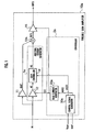
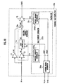
- a variable gain amplifier comprising: a first constant current amplifier configured to generate a reference current from an input signal; a second constant current amplifier configured to generate a constant current from the input signal; a first gain controller configured to generate a first addition current from the constant current; a first variable current amplifier configured to generate a first variable current from the input signal; a second gain controller configured to generate a second addition current from the first variable current; a second variable current amplifier configured to generate a second variable current from the input signal; a third gain controller configured to generate a third addition current from the second variable current; an adder configured to generate a first output signal by adding the reference current and the first to third addition currents; and a controller configured to generate a first bias current for controlling the first variable current, a second bias current for controlling the second variable current, a first control signal for controlling the first addition current, a second control signal for controlling the second addition current, and a third control signal for controlling the third addition current, and wherein an addition current generator is comprised by the first
- variable current amplifier 12 and the gain controller 14 are controlled at the same time, the distortion characteristic of the variable current AC increases because of the emitter resistance of each of the first V/I conversion transistor Q5 and the second V/I conversion transistor Q6.
- controller 2a shown in FIG 1 decreases variable current AC after decreasing the addition current AS when controlling a change from a high gain to a low gain, it is possible to maintain a good distortion characteristic.
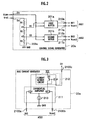
- the output controller 15d includes a first output controlling resistance R11, a second output controlling resistance R12, a third output controlling resistance R13, a fourth output controlling resistance R16, an output controlling transistor Q18, and an output controlling current source 151.
- the output controller 15d equalizes each of the positive second output signal OUT2+ and the negative second output signal OUT2- to the output current of the output controlling current source 151.
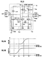
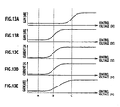
- FIGs. 1 to 9B An example in which the voltage gain of the variable gain amplifier 10a is decreased will be described.
- FIG 9A shows the gain of the gain controller 14 shown in FIG 1
- FIG. 9B shows the variable current AC.
- the power consumption of the entire variable gain amplifier 10a can be reduced because excess electric power is not consumed in periods of low gain. Furthermore, since the output current of the output amplifier 15 having a large power consumption is controlled by the bias current CI1, it is possible to reduce the power consumption of the variable gain amplifier 10a greatly. Moreover, since each output of the constant current amplifier 11, the variable current amplifier 12, and the gain controller 14 is current, it is possible to reduce the amount of resistance for generating voltage in the variable gain amplifier 10a.
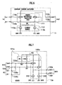
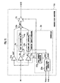
- FIGs. 11 to 13E An example in which the voltage gain of the entire variable gain amplifier 10c is controlled from a high gain to a low gain will be described. However, repeated descriptions for the same operation of the second embodiment which are the same as the first embodiment are omitted.
- FIG 13A shows the gain of second gain controller 14b shown in FIG 11
- FIG 13B shows the gain of first gain controller 14a
- FIG 13C shows the variable current AC
- FIG 13D shows the output current of the output amplifier 15
- FIG 13E shows the voltage gain of whole variable gain amplifier 10c.
- a controller 2c includes a control signal generator 20b, a first bias current generator 22c, and a second bias current generator 22d.
- the control signal generator 20b generates a first control signal AGS1, a second control signal AGS2, and a third control signal AGS3 based on the potential difference of the reference voltage Vref and the control voltage Vcon.
- the first bias current generator 22c generates a first bias current CI1 in accordance with the third control signal AGS3.
- the second bias current generator 22d generates a second bias current CI2 in accordance with the second control signal AGS2.
- variable gain amplifier 10d capable of operating with low power consumption. Furthermore, since each output of the second constant current amplifier 11b, the first variable current amplifier 12a, the second variable current amplifier 12b, the first gain controller 14a, the second gain controller 14b, and the third gain controller 14c is current, it is possible to reduce the amount of resistance for generating voltage in the variable gain amplifier 10d.
Landscapes
- Control Of Amplification And Gain Control (AREA)
Claims (16)
- Ein variabler Gewinnverstärker (10a, 10b, 10c, 10d, 10e), umfassend:einen ersten Konstantstromverstärker (11; 11a), der konfiguriert ist zum Erzeugen eines Referenzstroms (Aref) von einem Eingangssignal (IN);einen variablen Stromverstärker (12; 12a), der konfiguriert ist zum Erzeugen eines variablen Stroms (AC) von dem Eingangssignal;eine Gewinnsteuerungseinheit (14; 14a, 14b), die mit einem Ausgang des variablen Stromverstärkers verbunden ist und konfiguriert ist zum Erzeugen eines Additionsstroms (AS) von dem variablen Strom;einen Addierer (13a; 13b; 13c; 13d), der konfiguriert ist zum Erzeugen eines ersten Ausgangssignals (OUT1) durch Addieren des Referenzstroms (Aref) und des Additionsstroms (AS); undeine Steuerungseinheit (2a; 2b; 2c), die gesteuert wird durch eine Steuerungsspannung (Vcon) und die konfiguriert ist zum Erzeugen eines Bias-Stroms (CI1) zum Steuern des variablen Stroms (AC) und eines ersten Steuerungssignals (AGS1) zum Steuern des Additionsstroms (AS), wobei die Steuerungseinheit angepasst ist beim Steuern des Gewinns von einem hohen Gewinn zu einem niedrigen Gewinn zum Vermindern des Bias-Stroms (CI1) nach Vermindern des Gewinns durch Vermindern des Additionsstroms (AS) durch Verwenden des ersten Steuerungssignals (AGS1).
- Der variable Gewinnverstärker nach Anspruch 1, ferner umfassend einen Ausgangsverstärker (15), der konfiguriert ist zum Verstärken des ersten Ausgangssignals (OUT1), um ein zweites Ausgangssignal (OUT2) bereitzustellen.
- Der variable Gewinnverstärker nach Anspruch 2, wobei die Steuerungseinheit (2a) angepasst ist zum Vermindern eines Ausgangsstroms des Ausgangsverstärkers (15), wenn von einem hohen Gewinn zu einem niedrigen Gewinn gesteuert wird.
- Der variable Gewinnverstärker nach Anspruch 1, wobei der Addierer (13a) folgendes umfasst:einen Strom-Spannungs-Konverter (131a), der konfiguriert ist zum Erzeugen einer Spannung in Übereinstimmung mit einer Summe des Referenzstroms (Aref) und des Additionsstroms (AS); undeinen Spannungsausgabeschaltkreis (132a), der konfiguriert ist zum Erzeugen des ersten Ausgangssignals (OUT1) basierend auf der Spannung, die durch den Strom-Spannungs-Konverter (131a) erzeugt wird.
- Der variable Gewinnverstärker nach Anspruch 1, wobei der variable Stromverstärker (12) folgendes umfasst:eine variable Stromquelle (122), die konfiguriert ist zum Erzeugen eines Stroms in Übereinstimmung mit dem Bias-Strom (CI1); undein erstes differentielles Transistorpaar (121), das konfiguriert ist zum Erzeugen eines variablen Stroms (AC) durch Verstärken des Stroms, der von der variablen Stromquelle (122) zugeführt wird, in Übereinstimmung mit dem Eingangssignal (IN).
- Der variable Gewinnverstärker nach Anspruch 5, wobei die Gewinnsteuerungseinheit (14) zweite und dritte differentielle Transistorpaare (141, 142) umfasst, die konfiguriert sind zum Steuern des variablen Stroms (AC) in Übereinstimmung mit dem ersten Steuerungssignal (AGS1).
- Der variable Gewinnverstärker nach Anspruch 1, wobei die Steuerungseinheit (2a) folgendes umfasst:eine Steuerungssignalerzeugungseinheit (20a), die konfiguriert ist zum Erzeugen eines zweiten Steuerungssignals (AGS2) und des ersten Steuerungssignals (AGS1) basierend auf einer Potentialdifferenz einer Referenzspannung (Vref) und der Steuerungsspannung (Vcon); undeine Biasstromerzeugungseinheit (22a), die konfiguriert ist zum Erzeugen des Bias-Stroms (CI1) in Übereinstimmung mit dem zweiten Steuerungssignal (AGS2) .
- Der variable Gewinnverstärker nach Anspruch 7, wobei die Steuerungssignalerzeugungseinheit (20a) folgendes umfasst:einen Spannungsteiler (203a), der konfiguriert ist zum Erzeugen von ersten und zweiten Spannungen (V1, V2) durch Teilen der Referenzspannung (Vref);einen ersten Puffer (201a), der konfiguriert ist zum Erzeugen des ersten Steuerungssignals (AGS1) in Übereinstimmung mit der Potentialdifferenz der Steuerungsspannung (Vcon) und der ersten Spannung (V1) ; undeinen zweiten Puffer (201b), der konfiguriert ist zum Erzeugen des zweiten Steuerungssignals (AGS2) in Übereinstimmung mit der Potentialdifferenz der Steuerungsspannung (Vcon) und der zweiten Spannung (V2) .
- Der variable Gewinnverstärker nach Anspruch 7, wobei die Biasstromerzeugungseinheit (22a) folgendes umfasst:einen Stromspiegelschaltkreis (212), der konfiguriert ist zum Erzeugen des Bias-Stroms (CI1); undeinen differentiellen Verstärker (211), der konfiguriert ist zum Zuführen eines Stroms zu dem Stromspiegelschaltkreis (212) in Übereinstimmung mit dem zweiten Steuerungssignal (AGS2).
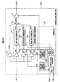
- Der variable Gewinnverstärker nach Anspruch 7, wobei die Additionsstromerzeugungseinheit (1b) folgendes umfasst:einen zweiten Konstantstromverstärker (11b), der konfiguriert ist zum Erzeugen eines Konstantstroms von dem Eingangssignal (IN);eine erste Gewinnsteuerungseinheit (14a), die konfiguriert ist zum Erzeugen eines ersten Additionsstroms (AS1) als den Additionsstrom durch Steuern des Konstantstroms in Übereinstimmung mit dem zweiten Steuerungssignal (AGS2);einen variablen Stromverstärker (12a), der konfiguriert ist zum Erzeugen des variablen Stroms (AC) basierend auf der Bias-Strom (CI1); undeine zweite Gewinnsteuerungseinheit (14b), die konfiguriert ist zum Erzeugen eines zweiten Additionsstroms (AS2) als den Additionsstrom durch Steuern des variablen Stroms (AC) in Übereinstimmung mit dem ersten Steuerungssignal (AGS1) .
- Der variable Gewinnverstärker nach Anspruch 10, wobei die Steuerungseinheit (2a) angepasst ist zum Vermindern des variablen Stroms (AC) und des ersten Additionsstroms (AS1) nach Vermindern des zweiten Additionsstroms (AS2) im Fall des Steuerns von einem hohen Gewinn zu einem niedrigen Gewinn.
- Der variable Gewinnverstärker nach Anspruch 1, wobei die Steuerungseinheit (2c) folgendes umfasst:eine Steuerungssignalerzeugungseinheit (20c), die konfiguriert ist zum Erzeugen einer Vielzahl von Steuerungssignalen (AGS1, ... AGS (n+1)) basierend auf der Potentialdifferenz einer Referenzspannung (Vref) und der Steuerungsspannung (Vcon); undeine Biasstromerzeugungseinheit (22a), die konfiguriert ist zum Erzeugen des Bias-Stroms (CI1) basierend auf dem Steuerungssignal (AGS(n+1)).
- Der variable Gewinnverstärker nach Anspruch 12, wobei die Additionsstromerzeugungseinheit (1d) folgendes umfasst:eine Vielzahl von variablen Stromverstärkern (12-1, ...12-n), die konfiguriert sind zum Erzeugen einer entsprechenden Anzahl von variablen Strömen (AC1, ... ACn) als den variablen Strom basierend auf dem Bias-Strom (CI1; undeine Vielzahl von Gewinnsteuerungseinheiten (14-1, ... 14-n), die konfiguriert sind zum Steuern der variablen Ströme (AC1, ... ACn) in Übereinstimmung mit den Steuerungssignalen (AGS1, ... AGSn) und zum Erzeugen einer Vielzahl von Additionsströmen (AS1, ... ASn) als den Additionsstrom.
- Ein variabler Gewinnverstärker (10d), umfassend:einen ersten Konstantstromverstärker (11a), der konfiguriert ist zum Erzeugen eines Referenzstroms (Aref) von einem Eingangssignal (IN);eine Additionsstromerzeugungseinheit, umfassend:einen zweiten Konstantstromverstärker (11b), der konfiguriert ist zum Erzeugen eines Konstantstroms (RA) von einem Eingangssignal (IN);eine erste Gewinnsteuerungseinheit (14a), die konfiguriert ist zum Erzeugen eines ersten Additionsstroms (AS1) von dem Konstantstrom (RA);einen ersten variablen Stromverstärker (12a), der konfiguriert ist zum Erzeugen eines ersten variablen Stroms (AC1) von dem Eingangssignal (IN);eine zweite Gewinnsteuerungseinheit (14b), die konfiguriert ist zum Erzeugen eines zweiten Additionsstroms (AS2) von dem variablen Strom (AC1);einen zweiten variablen Stromverstärker (12b), der konfiguriert ist zum Erzeugen eines zweiten variablen Stroms (AC2) von dem Eingangssignal (IN);eine dritte Gewinnsteuerungseinheit (14c), die konfiguriert ist zum Erzeugen eines dritten Additionsstroms (AS3) von dem zweiten variabeln Strom (AC2);wobei der variable Gewinnverstärker ferner folgendes umfasst:einen Addierer (13c), der konfiguriert ist zum Erzeugen eines ersten Ausgangssignals (OUT1) durch Addieren des Referenzstroms (Aref) und der ersten bis dritten Additionsströme (AS1, AS2, AS3); undeine Steuerungseinheit (2c), die konfiguriert ist zum Erzeugen eines ersten Bias-Stroms (CI1) zum Steuern des ersten variabeln Stroms (AC1), eines zweiten Bias-Stroms (CI2) zum Steuern des zweiten variablen Stroms (AC2), eines ersten Steuerungssignals (AGS3) zum Steuern des ersten Additionsstroms (AS1), eines zweiten Steuerungssignals (AGS2) zum Steuern des zweiten Additionsstroms (AS2), und eines dritten Steuerungssignals (AGS1) zum Steuern des dritten Additionsstroms (AS3), und wobeidie Steuerungseinheit (2c) angepasst ist zum Vermindern des dritten Additionsstroms (AS3), des zweiten Additionsstroms (AS2) und des ersten Additionsstroms (AS1) in dieser Reihenfolge, wenn der Gewinn von einem hohen Gewinn zu einem niedrigen Gewinn gesteuert wird.
- Der variable Gewinnverstärker nach Anspruch 14, wobei der Addierer folgendes umfasst:einen Strom-Spannungs-Konverter (131b), der konfiguriert ist zum Erzeugen einer Spannung in Übereinstimmung mit einer Summe des Referenzstroms (Aref) und der ersten bis dritten Additionsströme (AS1, AS2, AS3); undeinen Spannungsausgabeschaltkreis (132b), der konfiguriert ist zum Erzeugen des ersten Ausgangssignals (OUT1) basierend auf der Spannung, die durch den Strom-Spannungs-Konverter (131b) erzeugt wird.
- Der variable Gewinnverstärker nach Anspruch 14, wobei die Steuerungseinheit folgendes umfasst:eine Steuerungssignalerzeugungseinheit (20b), die konfiguriert ist zum Erzeugen der ersten bis dritten Steuerungssignale (AGS1, AGS2, AGS3) basierend auf einer Potentialdifferenz einer Referenzspannung (Vref) und der Steuerungsspannung (Vcon);eine erste Biasstromerzeugungseinheit (22c), die konfiguriert ist zum Erzeugen des ersten Bias-Stroms (CI1) in Übereinstimmung mit dem dritten Steuerungssignal (AGS1); undeine zweite Biasstromerzeugungseinheit (22d), die konfiguriert ist zum Erzeugen des zweiten Bias-Stroms (CI2) in Übereinstimmung mit dem zweiten Steuerungssignal (AGS2).
Applications Claiming Priority (2)
| Application Number | Priority Date | Filing Date | Title |
|---|---|---|---|
| JP2003362177 | 2003-10-22 | ||
| JP2003362177 | 2003-10-22 |
Publications (3)
| Publication Number | Publication Date |
|---|---|
| EP1526638A2 EP1526638A2 (de) | 2005-04-27 |
| EP1526638A3 EP1526638A3 (de) | 2007-07-04 |
| EP1526638B1 true EP1526638B1 (de) | 2011-08-31 |
Family
ID=34386508
Family Applications (1)
| Application Number | Title | Priority Date | Filing Date |
|---|---|---|---|
| EP04025100A Expired - Lifetime EP1526638B1 (de) | 2003-10-22 | 2004-10-21 | Verstärker mit variabler Verstärkung |
Country Status (3)
| Country | Link |
|---|---|
| US (1) | US7038542B2 (de) |
| EP (1) | EP1526638B1 (de) |
| CN (1) | CN100459427C (de) |
Cited By (1)
| Publication number | Priority date | Publication date | Assignee | Title |
|---|---|---|---|---|
| EP4214835A1 (de) * | 2020-10-07 | 2023-07-26 | Huawei Technologies Co., Ltd. | Verstärker mit variabler verstärkung |
Families Citing this family (10)
| Publication number | Priority date | Publication date | Assignee | Title |
|---|---|---|---|---|
| JP4543805B2 (ja) * | 2003-08-07 | 2010-09-15 | 富士通株式会社 | 差動増幅回路 |
| US7282996B2 (en) * | 2005-04-14 | 2007-10-16 | Micron Technology, Inc. | Electronic amplifier with signal gain dependent bias |
| RU2419197C1 (ru) * | 2010-02-02 | 2011-05-20 | Государственное образовательное учреждение высшего профессионального образования "Южно-Российский государственный университет экономики и сервиса" (ГОУ ВПО "ЮРГУЭС") | Дифференциальный усилитель с повышенным коэффициентом усиления по напряжению |
| CN103490738B (zh) * | 2013-07-01 | 2016-09-21 | 络达科技股份有限公司 | 可调增益放大器 |
| US9640231B1 (en) * | 2016-02-03 | 2017-05-02 | Qualcomm Incorporated | Shared sense amplifier |
| CN106208997B (zh) * | 2016-07-25 | 2019-04-12 | 北京工业大学 | 超宽带双重增益控制电路 |
| IT201600110367A1 (it) * | 2016-11-03 | 2018-05-03 | St Microelectronics Srl | Procedimento per il controllo di amplificatori, circuito e dispositivo corrispondenti |
| CN108259007B (zh) * | 2017-12-29 | 2021-06-04 | 思瑞浦微电子科技(苏州)股份有限公司 | 应用于运放转换速率的增强电路 |
| KR102734914B1 (ko) | 2019-06-17 | 2024-11-27 | 삼성전자주식회사 | 다이나믹 증폭기 |
| US11664814B2 (en) * | 2021-08-30 | 2023-05-30 | Analog Devices International Unlimited Company | Voltage interpolator |
Family Cites Families (14)
| Publication number | Priority date | Publication date | Assignee | Title |
|---|---|---|---|---|
| JP2766264B2 (ja) * | 1987-10-12 | 1998-06-18 | 株式会社東芝 | 差動増幅回路 |
| JP3170824B2 (ja) * | 1991-10-16 | 2001-05-28 | 松下電器産業株式会社 | オーディオ電力増幅器 |
| DE69323483T2 (de) * | 1993-04-06 | 1999-06-24 | Stmicroelectronics S.R.L., Agrate Brianza, Mailand/Milano | Veränderliche Verstärkungsregelung für Anordnungen mit niedriger Speisespannung |
| US6084466A (en) * | 1998-10-22 | 2000-07-04 | National Semiconductor Corporation | Variable gain current summing circuit with mutually independent gain and biasing |
| US6272336B1 (en) * | 1998-12-30 | 2001-08-07 | Samsung Electronics Co., Ltd. | Traffic-weighted closed loop power detection system for use with an RF power amplifier and method of operation |
| JP3534233B2 (ja) * | 1999-01-08 | 2004-06-07 | 松下電器産業株式会社 | 自動利得制御方法及びその装置、自動利得制御機能を持った無線通信装置 |
| US6255906B1 (en) * | 1999-09-30 | 2001-07-03 | Conexant Systems, Inc. | Power amplifier operated as an envelope digital to analog converter with digital pre-distortion |
| JP4014072B2 (ja) * | 2000-03-31 | 2007-11-28 | 株式会社ルネサステクノロジ | 電力増幅器モジュール |
| US6512416B2 (en) * | 2000-07-03 | 2003-01-28 | Broadcom Corporation | Extended range variable gain amplifier |
| JP2002076800A (ja) * | 2000-08-30 | 2002-03-15 | Nec Corp | 電圧減算・加算回路及びそれを実現するmos差動増幅回路 |
| US6683499B2 (en) * | 2000-12-27 | 2004-01-27 | Emhiser Research, Inc. | Divided-voltage fet power amplifiers |
| US6614300B2 (en) * | 2001-08-27 | 2003-09-02 | Nokia Corporation | Dual current mirror power amplifier bias control |
| JP2003188667A (ja) | 2001-12-17 | 2003-07-04 | Matsushita Electric Ind Co Ltd | 多段可変利得増幅器 |
| JP3942013B2 (ja) * | 2002-01-28 | 2007-07-11 | 株式会社ルネサステクノロジ | 通信用半導体集積回路および無線通信装置 |
-
2004
- 2004-10-20 US US10/968,008 patent/US7038542B2/en not_active Expired - Lifetime
- 2004-10-21 EP EP04025100A patent/EP1526638B1/de not_active Expired - Lifetime
- 2004-10-22 CN CNB2004100959787A patent/CN100459427C/zh not_active Expired - Fee Related
Cited By (1)
| Publication number | Priority date | Publication date | Assignee | Title |
|---|---|---|---|---|
| EP4214835A1 (de) * | 2020-10-07 | 2023-07-26 | Huawei Technologies Co., Ltd. | Verstärker mit variabler verstärkung |
Also Published As
| Publication number | Publication date |
|---|---|
| CN1610252A (zh) | 2005-04-27 |
| CN100459427C (zh) | 2009-02-04 |
| US7038542B2 (en) | 2006-05-02 |
| EP1526638A3 (de) | 2007-07-04 |
| US20050110571A1 (en) | 2005-05-26 |
| EP1526638A2 (de) | 2005-04-27 |
Similar Documents
| Publication | Publication Date | Title |
|---|---|---|
| KR101061953B1 (ko) | 가변 이득 증폭기 시스템 | |
| US6967535B2 (en) | High frequency power amplifier circuit | |
| US7595694B2 (en) | Electronics parts for high frequency power amplifier | |
| US5043672A (en) | Power detector utilizing bias voltage divider for precision control of an amplifier | |
| US20030169089A1 (en) | High linearity gilbert i q dual mixer | |
| US5872475A (en) | Variable attenuator | |
| EP1526638B1 (de) | Verstärker mit variabler Verstärkung | |
| US7109796B2 (en) | Amplifying circuit with adjustable amplification and transmitter system comprising such an amplifying circuit | |
| KR20000005825A (ko) | 전력증폭회로와안정화회로를구비하는무선주파수장치와,이러한장치를구비하는이동트랜시버단말기 | |
| KR100397332B1 (ko) | 이동단말기에서 자동이득제어기의 온도보상회로 | |
| JP5064224B2 (ja) | デュアルバイアス制御回路 | |
| JPH09135131A (ja) | 可変利得増幅器 | |
| US6744308B1 (en) | System and method for establishing the input impedance of an amplifier in a stacked configuration | |
| US6542045B2 (en) | High-frequency variable attenuator having a controllable reference voltage | |
| EP1537651A1 (de) | System und verfahren zur herstellung eines vorstroms unter verwendung einer rückkopplungsschleife | |
| US6078219A (en) | Wide range single stage variable gain amplifier | |
| KR100295678B1 (ko) | 선형 이득제어 증폭기 | |
| US7126424B2 (en) | Interface circuit for connecting to an output of a frequency converter | |
| JP4389360B2 (ja) | 利得制御装置 | |
| JP4031472B2 (ja) | 可変利得増幅器 | |
| US7015758B2 (en) | Gain control circuit, and a radio communication apparatus using the same | |
| JPH10327025A (ja) | 広帯域増幅器回路を含む装置 | |
| US7652509B2 (en) | Differential input and output transconductance circuit | |
| US6388529B2 (en) | Grounded emitter amplifier and a radio communication device using the same | |
| US6980052B1 (en) | Low-voltage pre-distortion circuit for linear-in-dB variable-gain cells |
Legal Events
| Date | Code | Title | Description |
|---|---|---|---|
| PUAI | Public reference made under article 153(3) epc to a published international application that has entered the european phase |
Free format text: ORIGINAL CODE: 0009012 |
|
| 17P | Request for examination filed |
Effective date: 20041021 |
|
| AK | Designated contracting states |
Kind code of ref document: A2 Designated state(s): AT BE BG CH CY CZ DE DK EE ES FI FR GB GR HU IE IT LI LU MC NL PL PT RO SE SI SK TR |
|
| AX | Request for extension of the european patent |
Extension state: AL HR LT LV MK |
|
| PUAL | Search report despatched |
Free format text: ORIGINAL CODE: 0009013 |
|
| AK | Designated contracting states |
Kind code of ref document: A3 Designated state(s): AT BE BG CH CY CZ DE DK EE ES FI FR GB GR HU IE IT LI LU MC NL PL PT RO SE SI SK TR |
|
| AX | Request for extension of the european patent |
Extension state: AL HR LT LV MK |
|
| 17Q | First examination report despatched |
Effective date: 20071008 |
|
| AKX | Designation fees paid |
Designated state(s): DE GB NL |
|
| GRAP | Despatch of communication of intention to grant a patent |
Free format text: ORIGINAL CODE: EPIDOSNIGR1 |
|
| GRAS | Grant fee paid |
Free format text: ORIGINAL CODE: EPIDOSNIGR3 |
|
| GRAA | (expected) grant |
Free format text: ORIGINAL CODE: 0009210 |
|
| AK | Designated contracting states |
Kind code of ref document: B1 Designated state(s): DE GB NL |
|
| REG | Reference to a national code |
Ref country code: GB Ref legal event code: FG4D |
|
| REG | Reference to a national code |
Ref country code: DE Ref legal event code: R096 Ref document number: 602004034182 Country of ref document: DE Effective date: 20111103 |
|
| REG | Reference to a national code |
Ref country code: NL Ref legal event code: T3 |
|
| PLBE | No opposition filed within time limit |
Free format text: ORIGINAL CODE: 0009261 |
|
| STAA | Information on the status of an ep patent application or granted ep patent |
Free format text: STATUS: NO OPPOSITION FILED WITHIN TIME LIMIT |
|
| 26N | No opposition filed |
Effective date: 20120601 |
|
| REG | Reference to a national code |
Ref country code: DE Ref legal event code: R097 Ref document number: 602004034182 Country of ref document: DE Effective date: 20120601 |
|
| PGFP | Annual fee paid to national office [announced via postgrant information from national office to epo] |
Ref country code: DE Payment date: 20151013 Year of fee payment: 12 Ref country code: GB Payment date: 20151021 Year of fee payment: 12 |
|
| PGFP | Annual fee paid to national office [announced via postgrant information from national office to epo] |
Ref country code: NL Payment date: 20151012 Year of fee payment: 12 |
|
| REG | Reference to a national code |
Ref country code: DE Ref legal event code: R119 Ref document number: 602004034182 Country of ref document: DE |
|
| REG | Reference to a national code |
Ref country code: NL Ref legal event code: MM Effective date: 20161101 |
|
| GBPC | Gb: european patent ceased through non-payment of renewal fee |
Effective date: 20161021 |
|
| PG25 | Lapsed in a contracting state [announced via postgrant information from national office to epo] |
Ref country code: GB Free format text: LAPSE BECAUSE OF NON-PAYMENT OF DUE FEES Effective date: 20161021 Ref country code: DE Free format text: LAPSE BECAUSE OF NON-PAYMENT OF DUE FEES Effective date: 20170503 |
|
| PG25 | Lapsed in a contracting state [announced via postgrant information from national office to epo] |
Ref country code: NL Free format text: LAPSE BECAUSE OF NON-PAYMENT OF DUE FEES Effective date: 20161101 |