EP1526638A2 - Verstärker mit variabler Verstärkung - Google Patents
Verstärker mit variabler Verstärkung Download PDFInfo
- Publication number
- EP1526638A2 EP1526638A2 EP04025100A EP04025100A EP1526638A2 EP 1526638 A2 EP1526638 A2 EP 1526638A2 EP 04025100 A EP04025100 A EP 04025100A EP 04025100 A EP04025100 A EP 04025100A EP 1526638 A2 EP1526638 A2 EP 1526638A2
- Authority
- EP
- European Patent Office
- Prior art keywords
- current
- variable
- generate
- amplifier
- voltage
- Prior art date
- Legal status (The legal status is an assumption and is not a legal conclusion. Google has not performed a legal analysis and makes no representation as to the accuracy of the status listed.)
- Granted
Links
- 230000007423 decrease Effects 0.000 claims description 28
- 230000003247 decreasing effect Effects 0.000 claims description 23
- 239000000872 buffer Substances 0.000 claims description 14
- 238000006243 chemical reaction Methods 0.000 description 20
- 238000010586 diagram Methods 0.000 description 19
- 102100022874 Dexamethasone-induced Ras-related protein 1 Human genes 0.000 description 13
- 101710150629 Dynein light chain Tctex-type 1 Proteins 0.000 description 13
- 101000620808 Homo sapiens Dexamethasone-induced Ras-related protein 1 Proteins 0.000 description 13
- 101000830956 Homo sapiens Three-prime repair exonuclease 1 Proteins 0.000 description 13
- 102100039474 Ribonuclease H2 subunit B Human genes 0.000 description 13
- 102100023940 G-protein-signaling modulator 1 Human genes 0.000 description 6
- 101000904748 Homo sapiens G-protein-signaling modulator 1 Proteins 0.000 description 6
- 101000670585 Homo sapiens Ribonuclease H2 subunit C Proteins 0.000 description 6
- 230000003321 amplification Effects 0.000 description 6
- 238000003199 nucleic acid amplification method Methods 0.000 description 6
- 238000013459 approach Methods 0.000 description 4
- 239000003990 capacitor Substances 0.000 description 4
- 230000004048 modification Effects 0.000 description 4
- 238000012986 modification Methods 0.000 description 4
- 239000004065 semiconductor Substances 0.000 description 4
- 230000005669 field effect Effects 0.000 description 2
- 239000000203 mixture Substances 0.000 description 2
- 230000001413 cellular effect Effects 0.000 description 1
- 239000006185 dispersion Substances 0.000 description 1
- 230000006698 induction Effects 0.000 description 1
- 230000003068 static effect Effects 0.000 description 1
Images


Classifications
-
- H—ELECTRICITY
- H03—ELECTRONIC CIRCUITRY
- H03G—CONTROL OF AMPLIFICATION
- H03G3/00—Gain control in amplifiers or frequency changers
- H03G3/20—Automatic control
- H03G3/30—Automatic control in amplifiers having semiconductor devices
- H03G3/3036—Automatic control in amplifiers having semiconductor devices in high-frequency amplifiers or in frequency-changers
- H03G3/3042—Automatic control in amplifiers having semiconductor devices in high-frequency amplifiers or in frequency-changers in modulators, frequency-changers, transmitters or power amplifiers
-
- H—ELECTRICITY
- H03—ELECTRONIC CIRCUITRY
- H03G—CONTROL OF AMPLIFICATION
- H03G1/00—Details of arrangements for controlling amplification
- H03G1/0005—Circuits characterised by the type of controlling devices operated by a controlling current or voltage signal
- H03G1/0017—Circuits characterised by the type of controlling devices operated by a controlling current or voltage signal the device being at least one of the amplifying solid-state elements
- H03G1/0023—Circuits characterised by the type of controlling devices operated by a controlling current or voltage signal the device being at least one of the amplifying solid-state elements in emitter-coupled or cascode amplifiers
-
- H—ELECTRICITY
- H03—ELECTRONIC CIRCUITRY
- H03G—CONTROL OF AMPLIFICATION
- H03G3/00—Gain control in amplifiers or frequency changers
- H03G3/20—Automatic control
- H03G3/30—Automatic control in amplifiers having semiconductor devices
- H03G3/3036—Automatic control in amplifiers having semiconductor devices in high-frequency amplifiers or in frequency-changers
- H03G3/3042—Automatic control in amplifiers having semiconductor devices in high-frequency amplifiers or in frequency-changers in modulators, frequency-changers, transmitters or power amplifiers
- H03G3/3047—Automatic control in amplifiers having semiconductor devices in high-frequency amplifiers or in frequency-changers in modulators, frequency-changers, transmitters or power amplifiers for intermittent signals, e.g. burst signals
Definitions
- the present invention relates to a variable gain amplifier used for radio terminals.
- Radio terminals such as a cellular phone include a variable gain amplifier having variable voltage gain in the transmitter and the receiver.
- a variable gain amplifier having variable voltage gain in the transmitter and the receiver.
- CDMA code division multiple access
- more than 80 [dB] variable gain width is required for a variable gain amplifier because many terminals use the same frequency band. Since the variable gain width of an amplifier is from 20 to 30 [dB], it is common to configure the variable gain amplifier by combining a plurality of amplifiers.
- providing variable gain amplifiers capable of operating with low power consumption is desired, because the power consumption of the radio terminals is limited.
- multistage variable gain amplifiers composed of an amplifier having variable voltage gain and an amplifier having variable output current has been proposed.
- each amplifier having variable voltage gain and the amplifier having variable output current includes a plurality of resistances for generating voltage.
- An aspect of the present invention provides a variable gain amplifier including a first constant current amplifier configured to generate a reference current from an input signal, a controller configured to generate a bias current and a first control signal based on a control voltage, an addition current generator configured to generate a variable current from the input signal based on the bias current, and to generate an addition current by controlling the variable current in accordance with the first control signal, and an adder configured to generate a first output signal by adding the reference current and the addition current.
- variable gain amplifier including a first constant current amplifier configured to generate a reference current from an input signal, a controller configured to generate first and second bias currents and first to third control signals based on a control voltage, an addition current generator configured to generate first to third addition currents based on the first and second bias currents and the first to third control signals, and an adder configured to generate a first output signal by adding the reference current and the first to third addition currents.
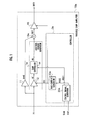
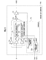
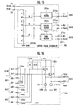
- a variable gain amplifier 10a includes a constant current amplifier 11, an addition current generator 1a, an adder 13a, a controller 2a, and an output amplifier 15.
- the constant current amplifier 11 generates a reference current Aref from an input signal IN.
- the controller 2a generates a bias current CI1 and a first control signal AGS1 based on a control voltage Vcon.
- the addition current generator 1a generates a variable current AC from the input signal IN based on the bias current CI1, and generates an addition current AS by controlling the variable current AC in accordance with first control signal AGS1.
- the adder 13a generates a first output signal OUT1 by adding the reference current Aref and the addition current AS.
- the output amplifier 15 generates a second output signal OUT2 by amplifying the first output signal OUT1.
- the constant current amplifier 11, the addition current generator 1a, the controller 2a, the adder 13a, and the output amplifier 15 are configured as differential circuits, for example.
- the control voltage Vcon is supplied by a base band unit (not illustrated), for example.
- the controller 2a decreases the variable current AC after decreasing the the addition current AS when the voltage gain of the variable gain amplifier 10a is controlled from a high gain to a low gain. Specifically, the controller 2a decreases the output direct current component of variable current amplifier 12.
- the ratio of the reference current Aref to the maximum variable current AC is 1:3. The variable current AC becomes zero when the variable gain amplifier 10a is a minimum gain.
- the controller 2a increases the addition current AS after increasing the variable current AC when controlling from a low gain to a high gain.
- the controller 2a includes a control signal generator 20a and a bias current generator 22a.
- the control signal generator 20a generates a first control signal AGS1 and a second control signal AGS2 in accordance with the potential difference of the control voltage Vcon and a reference voltage Vref having a constant voltage value.
- the bias current generator 22a generates the bias current CI1 in accordance with the second control signal AGS2.
- the bias current CI1 is supplied to the variable current amplifier 12 and the output amplifier 15.
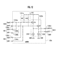
- the control signal generator 20a includes a control voltage terminal 3b, a reference voltage terminal 3c, a first converted voltage output terminal 210a, a first converted control voltage output terminal 211 a, a second converted voltage output terminal 210b, a second converted control voltage output terminal 211b, a voltage divider 203a, a first buffer 201a, and a second buffer 201b.
- the voltage divider 203a generates a first voltage V1 and a second voltage V2 by dividing the reference voltage Vref.
- the first buffer 201a generates first converted voltage BV1 and first converted control voltage Vcon1 based on the potential difference of the first voltage V1 and the control voltage Vcon.
- the first converted voltage BV1 and the first converted control voltage Vcon1 configure a first control signal AGS1.
- the second buffer 201b generates a second converted voltage BV2 and a second converted control voltage Vcon2 based on the potential difference of the second voltage V2 and the control voltage Vcon.
- the second converted voltage BV1 and the second converted control voltage Vcon2 configure a second control signal AGS2.
- the voltage divider 203a includes a first dividing-resistance R1 connected to the reference voltage terminal 3c, a second dividing-resistance R2 connected to the first dividing-resistance R1, and a third dividing-resistance R3 connected between the second dividing-resistance R2 and a ground GND.
- the first buffer 201a has an input side connected to a connection node n1, and an output side connected to the first converted voltage output terminal 210a and the first converted control voltage output terminal 211a.
- the second buffer 201b has an input side connected to a connection node n2, and an output side connected to the second converted voltage output terminal 210b and the second converted control voltage output terminal 211b.
- the bias current generator 22a includes a first current controlling input terminal 2100a, a second current controlling input terminal 2100b, a bias current output terminal 2100c, a differential amplifier 211, and a current mirror circuit 212.
- the differential amplifier 211 supplies a current to the current mirror circuit 212 in accordance with the potential difference of the second converted voltage BV2 and the second converted control voltage Vcon2.
- the current mirror circuit 212 generates the bias current CI1 based on the current from the differential amplifier 211.
- the differential amplifier 211 includes a first differential transistor Q1, a second differential transistor Q2, and a constant current source 213.
- the first differential transistor Q1 has a collector connected to a power supply VCC, a base connected to the first current controlling input terminal 2100, and an emitter connected to the constant current source 213.
- the second differential transistor Q2 has a collector connected to the current mirror circuit 212, a base connected to second current controlling input terminal 2100b, and an emitter connected to the constant current source 213.
- the constant current source 213 is connected between each emitter of the first differential transistor Q1 and the second differential transistor Q2 and the ground GND.
- npn bipolar junction transistors can be used as the first differential transistor Q1 and the second differential transistor Q2.
- the current mirror circuit 212 includes a first mirror transistor Q3 and a second mirror transistor Q4.
- the first mirror transistor Q3 has an emitter connected to the power supply VCC, a base connected to the base of the second mirror transistor Q4, and a collector connected to the collector of the second differential transistor Q2. Furthermore, the collector of the first mirror transistor Q3 is connected to the base of the second mirror transistor Q4.
- the second mirror transistor Q4 has an emitter connected to the power supply VCC, a collector connected to the bias current output terminal 2100c.
- pnp bipolar junction transistors can be used as the first mirror transistor Q3 and the second mirror transistor Q4.
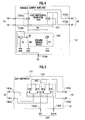
- the addition current generator 1a shown in FIG 1 includes a variable current amplifier 12, and a gain controller 14 connected to the variable current amplifier 12.
- the variable current amplifier 12 generates the variable current AC based on the bias current CI1.
- the gain controller 14 generates the addition current AS by controlling the variable current AC in accordance with the first control signal AGS1.
- the variable current amplifier 12 includes a first input terminal 120a, a second input terminal 120b, a current controlling terminal 120c, a first variable current output terminal 120d, a second variable current output terminal 120e, a first differential transistor pair 121, a first degenerate resistance R4, and a variable current source 122.
- the first degenerate resistance R4 is used for expanding the input level range of the variable current amplifier 12.
- the variable current source 122 generates a current in accordance with the bias current CI1.
- the first differential transistor pair 121 controls the current from the variable current source 122 in accordance with the potential difference of a positive input signal In+ and a negative input signal In- having an opposite phase of the positive input signal In+, and generates a positive variable current AC+ and a negative variable current AC- composing the variable current AC.
- the current waveform of the variable current AC becomes a merged waveform of a direct current generated by the variable current source 122 with a signal generated by the first differential transistor pair 121.
- the first differential transistor pair 121 includes a first voltage-current (V/I) conversion transistor Q5 and a second V/I conversion transistor Q6.
- the first V/I conversion transistor Q5 has a collector connected to the first variable current output terminal 120d, and a base connected to the first input terminal 120a.
- the second V/I conversion transistor Q6 has a collector connected to the second variable current output terminal 120e, and a base connected to the second input terminal 120b.
- the first degenerate resistance R4 is connected between each emitter of the first V/I conversion transistor Q5 and the second V/I conversion transistor Q6.
- variable current amplifier 12 and the gain controller 14 are controlled at the same time, the distortion characteristic of the variable current AC increases because of the emitter resistance of each of the first V/I conversion transistor Q5 and the second V/I conversion transistor Q6.
- controller 2a shown in FIG 1 decreases variable current AC after decreasing the addition current AS when controlling a change from a high gain to a low gain, it is possible to maintain a good the distortion characteristic.
- the variable current source 122 is configured as a current mirror circuit.
- the variable current source 122 includes a first current setting transistor Q7, a second current setting transistor Q8, a third current setting transistor Q9, a first current setting resistance R5, a second current setting resistance R6, and a third current setting resistance R7.
- the first current setting resistance R5, the second current setting resistance R6, and the third current setting resistance R7 are connected to the ground GND.
- the first current setting transistor Q7 has a collector and a base connected to the current controlling terminal 120c, and an emitter connected to the first current setting resistance R5.
- the second current setting transistor Q8 has a collector connected to the emitter of the first V/I conversion transistor Q5, a base connected to the base of the first current setting transistor Q7, and an emitter connected to the second current setting resistance R6.
- the third current setting transistor Q9 has a collector connected to the emitter of the second V/I conversion transistor Q6, a base connected to the base of the first current setting transistor Q7, and an emitter connected to the third current setting resistance R7.
- npn bipolar junction transistors can be used as the first V/I conversion transistor Q5, the second V/I conversion transistor Q6, the first current setting transistor Q7, the second current setting transistor Q8, and the third current setting transistor Q9.
- the gain controller 14 includes a first variable current input terminal 140a, a second variable current input terminal 140b, a first addition current output terminal 140c, a second addition current output terminal 140d, a first converted voltage input terminal 140e, a first converted control voltage input terminal 140f, a second differential transistor pair 141, and a third differential transistor pair 142.
- the second differential transistor pair 141 When the voltage value of the first converted control voltage Vcon1 is larger than the voltage value of the first converted voltage BV1, the second differential transistor pair 141 generates a positive addition current AS+ of the addition current AS by amplifying the positive variable current AC+.
- the third differential transistor pair 142 generates a negative addition current AS- of the addition current AS by amplifying the negative variable current AC-.
- the second differential transistor pair 141 includes a first gain controlling transistor Q10 and a second gain controlling transistor Q11.
- the first gain controlling transistor Q10 has a collector connected to the first addition variable current output terminal 140c, a base connected to the first converted control voltage input terminal 140f, and an emitter connected to the first variable current input terminal 140a.
- the second gain controlling transistor Q11 has a collector connected to the power supply VCC, a base connected to the first converted voltage input terminal 140e, and an emitter connected to first addition current input terminal 140a.
- the third differential transistor pair 142 includes a third gain controlling transistor Q12 and a fourth gain controlling transistor Q13.
- the third gain controlling transistor Q12 has a collector connected to the power supply VCC, a base connected to the first converted voltage input terminal 140e, and an emitter connected to the second variable current input terminal 140b.
- the fourth gain controlling transistor Q13 has a collector connected to the second addition current output terminal 140d, a base connected to the first converted control voltage input terminal 140f, and an emitter connected to the second addition current input terminal 140b.
- npn bipolar junction transistors can be used as the first to fourth gain controlling transistors Q10 to Q13.
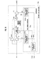
- the constant current amplifier 11 includes a third input terminal 110a, a fourth input terminal 110b, a first reference current output terminal 110c, a second reference current output terminal 110d, a fourth differential transistor pair 111, a second degenerate resistance R8, and a current source 112.
- the current source 112 supplies a current to the fourth differential transistor pair 111.
- the fourth differential transistor pair 111 generates a positive reference current Aref+ and a negative reference current Aref- configuring the reference current Aref based on the positive input signal In+ and negative input signal In-.
- the second degenerate resistance R8 sets an input level range of the fourth differential transistor pair 111.
- the resistance value of the second degenerate resistance R8 is set larger than the resistance value of the first degenerate resistance R4 shown in FIG 4.
- the current source 112 includes a first current source 112a and a second current source 112b connected to the ground GND.
- the fourth differential transistor pair 111 includes a third V/I conversion transistor Q14 and a fourth V/I conversion transistor Q15.
- the third V/I conversion transistor Q14 has a collector connected to the first reference current output terminal 110c, a base connected to the third input terminal 110a, and an emitter connected to the first current source 112a.
- the fourth V/I conversion transistor Q15 has a collector connected to the second reference current output terminal 110d, a base connected to the fourth input terminal 110b, and an emitter connected to the second current source 112b.
- the second degenerate resistance R8 is connected between the emitter of the third V/I conversion transistor Q14 and the emitter of the fourth V/I conversion transistor Q15.
- npn bipolar junction transistors can be used as the third V/I conversion transistor Q14 and the fourth V/I conversion transistor Q15.
- the adder 13a includes a first reference current input terminal 133a, a second reference current input terminal 134a, a first positive addition current input terminal 133b, a first negative addition current input terminal 134b, a first output terminal 130e, a second output terminal 130f, a current-voltage converter 131a, and a voltage outputting circuit 132a.
- the current-voltage converter 131a generates a first addition voltage VA+ in accordance with the sum of the positive reference current Aref+ and the positive addition current AS+, and generates second addition voltage VAin accordance with the sum of the negative reference current Aref- and the negative addition current AS-.
- the voltage outputting circuit 132a generates a positive output signal OUT1+ and a negative output signal OUT1- configuring the first output signal OUT1 based on the first addition voltage VA+ and the second addition voltage VA-.
- the current-voltage converter 131a includes a first voltage generating resistance R9 and a second voltage generating resistance R10.
- the first voltage generating resistance R9 has one end connected to the power supply VCC, and another end connected to the first reference current input terminal 133a and the first addition current input terminal 133b.
- the second voltage generating resistance R10 has one end connected to the power supply VCC, and another end connected to the second reference current input terminal 134a and the second addition current input terminal 134b.
- the voltage outputting circuit 132a is configured as an emitter follower circuit. That is, the voltage outputting circuit 132a includes a first outputting transistor Q16, a second outputting transistor Q17, a first outputting current source 232, and a second outputting current source 332.
- the first outputting current source 232 and the second outputting current source 332 are connected to the ground GND.
- the first outputting transistor Q16 has a collector connected to the power supply VCC, a base connected to the first reference current input terminal 133a and the first positive addition current input terminal 133b, and an emitter connected to the first outputting current source 232.
- the second outputting transistor Q17 has a collector connected to the power supply VCC, a base connected to the second reference current input terminal 134a and the second negative addition current input terminal 134b, and an emitter connected to the second outputting current source 332.
- npn bipolar junction transistors can be used as the first outputting transistor Q16 and the second outputting transistor Q17.
- the output amplifier 15 includes a first output signal terminal 150a, a second output signal terminal 150b, an outputting bias current terminal 150c, a first amplification output terminal 150d, a second amplification output terminal 150e, a tuning circuit 15a, a fifth differential transistor pair 15b, a outputting current source 15c, a output controller 15d, and a degenerate inductor L3.
- the tuning circuit 15a oscillates at a particular tuning frequency.
- the fifth differential transistor pair 15b generates a positive second output signal OUT2+ and a negative second output signal OUT2- configuring the second output signal OUT2 by selectively amplifying a signal component at the tuning frequency band of the tuning circuit 15a based on the positive output signal OUT1+ and the negative output signal OUT1-.
- the output controller 15d controls the positive second output signal OUT2+ and the negative second output signal OUT2- based on the bias current CI1.
- the outputting current source 15c includes a first current generating resistance R14 and a second current generating resistance R15 connected to the ground GND.
- the tuning circuit 15a includes two LC tuning circuits. That is, the tuning circuit 15a includes a first inductor L1 connected between the power supply VCC and the first amplification output terminal 150e, a first capacitor C1 connected in parallel with first inductor L1, a second inductor L2 connected between the power supply VCC and the second amplification output terminal 150d, and a second capacitor C2 connected in parallel with the second inductor L2.
- the first capacitor C1 and the second capacitor C2 may be omitted.
- the fifth differential transistor pair 15b includes a third outputting transistor Q19 and a fourth outputting transistor Q20.
- the third outputting transistor Q19 has a collector connected to the first amplification output terminal 150e, a base connected to the second output signal terminal 150b, and an emitter connected to the first current generating resistance R14.
- the fourth outputting transistor Q20 has a collector connected to the second amplification output terminal 150d, a base connected to the first output signal terminal 150a, and an emitter connected to the second current generating resistance R15.
- the degenerate inductor L3 is connected between the emitter of the third outputting transistor Q19 and the emitter of the fourth outputting transistor Q20.
- the output controller 15d includes a first output controlling resistance R11, a second output controlling resistance R12, a third output controlling resistance R13, a fourth output controlling resistance R16, an output controlling transistor Q18, and an output controlling current source 151.
- the output controller 15d equalizes each of the positive second output signal OUT2+ and the negative second output signal OUT2- to the output current of the output controlling current source 151.
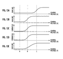
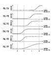
- FIGs. 1 to 9B An example in which the voltage gain of the variable gain amplifier 10a is decreased will be described.
- FIG 9A shows the gain of the gain controller 14 shown in FIG 1
- FIG. 9B shows the variable current AC.
- each collector current of the second current setting transistor Q8 and the third current setting transistor Q9 shown in FIG 4 is decreased gradually.
- each of the positive variable current AC+ and the negative variable current AC- is decreased.
- the output controller 15d shown in FIG 8 decreases the second output signal OUT2 in proportion to decrease in bias current CI1.
- each of the variable current AC and the bias current CI1 becomes zero when the voltage value of the control voltage Vcon is decreased until Va [V].
- the power consumption of the entire variable gain amplifier 10a can be reduced because excess electric power is not consumed in periods of low gain. Furthermore, since the output current of the output amplifier 15 having a large power consumption is controlled by the bias current CI1, it is possible to reduce the power consumption of the variable gain amplifier 10a greatly. Moreover, since each output of the constant current amplifier 11, the variable current amplifier 12, and the gain controller 14 is current, it is possible to reduce the amount of resistance for generating voltage in the variable gain amplifier 10a.
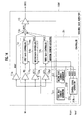
- a bias current generator 22b may include an addition current controller 220a and an output current controller 220b.
- the addition current controller 220a supplies a bias current CI1 to variable current amplifier 12 based on the second control signal AGS2.
- the output current controller 220b supplies a bias current CI2 to the output amplifier 15 based on the first control signal AGS1.
- the addition current controller 220a and the output current controller 220b are configured the same as the bias current generator 22a shown in FIG. 3.
- variable gain amplifier 10b it is possible to control the variable current amplifier 12 and the output amplifier 15 at a different timing. Therefore, it is possible to decrease the output current of the variable current amplifier 12 after decreasing the output current of the output amplifier 15 having a large output current.
- a variable gain amplifier 10c differs from the addition current generator 1a shown in FIG 1 in that an addition current generator 1b shown in FIG 11 includes a second constant current amplifier 11b, a first gain controller 14a, a variable current amplifier 12a, and a second gain controller 14b.
- the second constant current amplifier 11b generates a constant current RA from the input signal IN.
- the first gain controller 14a generates a first addition current AS1 by controlling the constant current RA in accordance with the second control signal AGS2.
- the variable current amplifier 12a generates a variable current AC based on the bias current CI1.
- the second gain controller 14b generates a second addition current AS2 by controlling the variable current AC in accordance with the first control signal AGS1.
- an adder 13b differs form the adder 13a shown in FIG 7 in that the adder 13b further includes a second positive addition current input terminal 133c, and a second negative addition current input terminal 134c.
- the maximum current of the variable current AC is larger than the constant current RA.
- Other components and configurations are similar to the variable gain amplifier 10a shown in FIG. 1.
- the controller 2a decreases the first addition current AS1 after decreasing the second addition current AS2 when the voltage gain of the variable gain amplifier 10c is controlled from a high gain to a low gain.
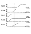
- FIGs. 11 to 13E An example in which the voltage gain of the entire variable gain amplifier 10c is controlled from a high gain to a low gain will be described. However, repeated descriptions for the same operation of the second embodiment which are the same as the first embodiment are omitted.
- FIG 13A shows the gain of second gain controller 14b shown in FIG 11
- FIG 13B shows the gain of first gain controller 14a
- FIG 13C shows the variable current AC
- FIG 13D shows the output current of the output amplifier 15
- FIG 13E shows the voltage gain of whole variable gain amplifier 10c.
- variable current AC it is possible to control the variable current AC to minimum, in periods of the low voltage gain of the variable gain amplifier 10c. Therefore, it is possible to provide the variable gain amplifier 10c which is capable of operating with low power consumption. Furthermore, since each output of the second constant current amplifier 11b, the variable current amplifier 12a, the first gain controller 14a, and the second gain controller 14b is current, it is possible to reduce the amount of resistance for generating voltage in the variable gain amplifier 10c.
- a controller 2c includes a control signal generator 20b, a first bias current generator 22c, and a second bias current generator 22d.
- the control signal generator 20b generates a first control signal AGS1, a second control signal AGS2, and a third control signal AGS3 based on the potential difference of the reference voltage Vref and the control voltage Vcon.
- the first bias current generator 22c generates a first bias current CI1 in accordance with the third control signal AGS3.
- the second bias current generator 22d generates a second bias current CI2 in accordance with the second control signal AGS2.
- the addition current generator 1c includes a second constant current amplifier 11b, a first gain controller 14a, a first variable current amplifier 12a, a second gain controller 14b, a second variable current amplifier 12b, and a third gain controller 14c.
- the second constant current amplifier 11b generates a constant current RA from the input signal IN.
- the first gain controller 14a generates a first addition current AS1 by controlling the constant current RA in accordance with the third control signal AGS3.
- the first variable current amplifier 12a generates a first variable current AC1 based on a first bias current CI1.
- the second gain controller 14b generates a second addition current AS2 by controlling the first variable current AC1 in accordance with the second control signal AGS2.
- the second variable current amplifier 12b generates a second variable current AC2 based on the second bias current.
- the third gain controller 14c generates a third addition current AS3 by controlling the second variable current AC2 in accordance with the first control signal AGS1.
- Other compositions are similar to the variable gain amplifier 10a shown in FIG. 1.
- control signal generator 20b further includes a third buffer 201c.
- the third buffer 201c generates the third control signal AGS3.
- the voltage divider 203b further includes a fourth dividing-resistance R4 connected between the third dividing-resistance R3 and the ground GND.
- the adder 13c further includes a second positive addition current input terminal 133c, a second negative addition current input terminal 134c, a third positive addition current input terminal 133d, and a third negative addition current input terminal 134d.
- FIGs. 14 to 17F An example in which the voltage gain of the entire variable gain amplifier 10d is controlled from a high gain to a low gain will be described. However, repeated descriptions for the same operation according to the third embodiment which are the same as the first and second embodiments are omitted.
- FIG 17A shows the gain of the third gain controller 14c shown in FIG 14
- FIG 17B shows the gain of the second gain controller 14b
- FIG. 17C shows the second variable current AC2
- FIG. 17D shows the gain of the first gain controller 14a
- FIG 17E shows the first variable current AC1
- FIG 17F shows the voltage gain of whole variable gain amplifier 10d.
- second bias current generator 22d shown in FIG. 14 decreases the output current of the second variable current amplifier 12b, that is, the second variable current AC2 based on the second control signal AGS2.
- variable gain amplifier 10d capable of operating with low power consumption. Furthermore, since each output of the second constant current amplifier 11b, the first variable current amplifier 12a, the second variable current amplifier 12b, the first gain controller 14a, the second gain controller 14b, and the third gain controller 14c is current, it is possible to reduce the amount of resistance for generating voltage in the variable gain amplifier 10d.
- a variable gain amplifier 10e differs from the variable gain amplifier 10a shown in FIG. 1 in that the addition current generator 1d includes first to n-th variable current amplifiers 12-1 to 12-n, and first to n-th gain controller 14-1 to 14-n connected to the first to n-th variable current amplifiers 12-1 to 12-n (n being an integer equal to or greater than 2).
- a controller 2c differs from the controller 2a shown in FIG. 1 in that the controller 2c supplies first to n-th gain control signals AGS1 to AGSn to the first to n-th gain controllers 14-1 to 14-n.
- the first to n-th variable current amplifiers 12-1 to 12-n generate first to n-th variable currents AC1 to ACn based on the bias current CI1.
- the first to n-th gain controllers 14-1 to 14-n generate first to n-th addition currents AS1 to ASn by controlling the first to n-th variable currents AC1 to ACn based on the first to n-th control signals AGS1 to AGSn.
- the control signal generator 20c supplies the (n+1)-th control signal AGS(n+1) to the bias current generator 22a.
- Other compositions are similar to the variable gain amplifier 10a shown in FIG. 1.
- Each maximum output current of the first to n-th variable current amplifiers 12-1 to 12-n is set as the first variable current amplifier 12-1 ⁇ the second variable current amplifier 12-2 ⁇ the third variable current amplifier 12-3 ⁇ ....
- the control signal generator 20c includes first to (n+1)-th buffers 201-1 to 201-(n+1).
- the voltage divider 203c includes first to (n+2)-th dividing-resistances R1 to R(n+2).
- the adder 13d has a configuration capable of dealing with the first to n-th addition currents AS1 to ASn.
- variable gain amplifier 10e includes the first variable current amplifier 12-1, the second variable current amplifier 12-2, the first gain controller 14-1, and the second gain controller 14-2. Repeated descriptions for the same operation according to the second embodiment which are the same as the first embodiment are omitted.
- FIG 21A shows the gain of the second gain controller 14-2
- FIG 21B shows the gain of the first gain controller 14-1
- FIG 21C shows the second variable current AC2
- FIG 21D shows the first variable current AC1
- FIG 21E shows the voltage gain of whole variable gain amplifier 10e.
- the bias current generator 22a shown in FIG 18 decreases the output current of the first variable current amplifier 12-1 and the second variable current amplifier 12-2, that is, the first variable current AC1 and the second variable current AC2. As shown in FIG 21D, the bias current generator 22a decreases the output current of the output amplifier 15.
- variable gain amplifier 10e it is possible to reduce the power consumption of the first to n-th variable current amplifiers 12-1 to 12-n in periods of low voltage gain of the variable gain amplifier 10e. Moreover, it is possible to reduce the number of the resistances for generating voltages.
- the second buffer 201b shown in FIG 2 may be arranged outside of the control signal generator 20d.
- the second buffer 201b shown in FIG 22 receives the voltage V2 and the control voltage Vcon from the exterior circuit. Accordingly, it is possible to control the bias current CI1 by controlling the voltage value of the voltage V2.
- a part of the buffers may be controlled directly from the exterior circuit.
- each resistance value of the first dividing-resistance R1, the second dividing-resistance R2, and the third dividing-resistance R3 configuring the voltage divider 203a shown in FIG 2 is fixed.
- variable resistances can be used as the first dividing-resistance R1, the second dividing-resistance R2, and the third dividing-resistance R3.
- variable gain amplifier 10a In the aforementioned variable gain amplifier 10a according to the first embodiment, description was given of an example in which the constant current amplifier 11, the addition current generator 1a, the controllers 2a and 2b, the adder 13a, and the output amplifier 15 are configured as differential circuits. However, it is possible to use only one transistor of the differential transistor pair included in the constant current amplifier 11, the addition current generator 1a, the controllers 2a and 2b, the adder 13a, and the output amplifier 15. Similarly, it can be adapted to the variable gain amplifiers 10c to 10e according to the second to fourth embodiments.
- variable gain amplifiers 10a to 10e according to the first to fourth embodiment can be monolithically integrated on a chip so as to form a semiconductor integrated circuit on a single semiconductor chip.
- bipolar junction transistors are used as the transistors included in the variable gain amplifiers 10a to 10e according to the first to fourth embodiments.
- various transistors can be used such as junction field effect transistors (JFET), metal-semiconductor field effect transistors (MESFET), static induction transistors (SIT), and high electron mobility transistors (HEMT).
- JFET junction field effect transistors
- MESFET metal-semiconductor field effect transistors
- SIT static induction transistors
- HEMT high electron mobility transistors
Landscapes
- Control Of Amplification And Gain Control (AREA)
Applications Claiming Priority (2)
| Application Number | Priority Date | Filing Date | Title |
|---|---|---|---|
| JP2003362177 | 2003-10-22 | ||
| JP2003362177 | 2003-10-22 |
Publications (3)
| Publication Number | Publication Date |
|---|---|
| EP1526638A2 true EP1526638A2 (de) | 2005-04-27 |
| EP1526638A3 EP1526638A3 (de) | 2007-07-04 |
| EP1526638B1 EP1526638B1 (de) | 2011-08-31 |
Family
ID=34386508
Family Applications (1)
| Application Number | Title | Priority Date | Filing Date |
|---|---|---|---|
| EP04025100A Expired - Lifetime EP1526638B1 (de) | 2003-10-22 | 2004-10-21 | Verstärker mit variabler Verstärkung |
Country Status (3)
| Country | Link |
|---|---|
| US (1) | US7038542B2 (de) |
| EP (1) | EP1526638B1 (de) |
| CN (1) | CN100459427C (de) |
Cited By (2)
| Publication number | Priority date | Publication date | Assignee | Title |
|---|---|---|---|---|
| IT201600110367A1 (it) * | 2016-11-03 | 2018-05-03 | St Microelectronics Srl | Procedimento per il controllo di amplificatori, circuito e dispositivo corrispondenti |
| WO2022073599A1 (en) * | 2020-10-07 | 2022-04-14 | Huawei Technologies Co., Ltd. | Variable gain amplifier |
Families Citing this family (9)
| Publication number | Priority date | Publication date | Assignee | Title |
|---|---|---|---|---|
| JP4543805B2 (ja) * | 2003-08-07 | 2010-09-15 | 富士通株式会社 | 差動増幅回路 |
| US7282996B2 (en) * | 2005-04-14 | 2007-10-16 | Micron Technology, Inc. | Electronic amplifier with signal gain dependent bias |
| RU2419197C1 (ru) * | 2010-02-02 | 2011-05-20 | Государственное образовательное учреждение высшего профессионального образования "Южно-Российский государственный университет экономики и сервиса" (ГОУ ВПО "ЮРГУЭС") | Дифференциальный усилитель с повышенным коэффициентом усиления по напряжению |
| CN103490738B (zh) * | 2013-07-01 | 2016-09-21 | 络达科技股份有限公司 | 可调增益放大器 |
| US9640231B1 (en) * | 2016-02-03 | 2017-05-02 | Qualcomm Incorporated | Shared sense amplifier |
| CN106208997B (zh) * | 2016-07-25 | 2019-04-12 | 北京工业大学 | 超宽带双重增益控制电路 |
| CN108259007B (zh) * | 2017-12-29 | 2021-06-04 | 思瑞浦微电子科技(苏州)股份有限公司 | 应用于运放转换速率的增强电路 |
| KR102734914B1 (ko) | 2019-06-17 | 2024-11-27 | 삼성전자주식회사 | 다이나믹 증폭기 |
| US11664814B2 (en) * | 2021-08-30 | 2023-05-30 | Analog Devices International Unlimited Company | Voltage interpolator |
Citations (2)
| Publication number | Priority date | Publication date | Assignee | Title |
|---|---|---|---|---|
| US20030102924A1 (en) | 2000-03-31 | 2003-06-05 | Hidetoshi Matsumoto | Power amplifier module |
| US20030141932A1 (en) | 2002-01-28 | 2003-07-31 | Kenji Toyota | Communication semiconductor integrated circuit device and wireless communication system |
Family Cites Families (12)
| Publication number | Priority date | Publication date | Assignee | Title |
|---|---|---|---|---|
| JP2766264B2 (ja) * | 1987-10-12 | 1998-06-18 | 株式会社東芝 | 差動増幅回路 |
| JP3170824B2 (ja) * | 1991-10-16 | 2001-05-28 | 松下電器産業株式会社 | オーディオ電力増幅器 |
| DE69323483T2 (de) * | 1993-04-06 | 1999-06-24 | Stmicroelectronics S.R.L., Agrate Brianza, Mailand/Milano | Veränderliche Verstärkungsregelung für Anordnungen mit niedriger Speisespannung |
| US6084466A (en) * | 1998-10-22 | 2000-07-04 | National Semiconductor Corporation | Variable gain current summing circuit with mutually independent gain and biasing |
| US6272336B1 (en) * | 1998-12-30 | 2001-08-07 | Samsung Electronics Co., Ltd. | Traffic-weighted closed loop power detection system for use with an RF power amplifier and method of operation |
| JP3534233B2 (ja) * | 1999-01-08 | 2004-06-07 | 松下電器産業株式会社 | 自動利得制御方法及びその装置、自動利得制御機能を持った無線通信装置 |
| US6255906B1 (en) * | 1999-09-30 | 2001-07-03 | Conexant Systems, Inc. | Power amplifier operated as an envelope digital to analog converter with digital pre-distortion |
| US6512416B2 (en) * | 2000-07-03 | 2003-01-28 | Broadcom Corporation | Extended range variable gain amplifier |
| JP2002076800A (ja) * | 2000-08-30 | 2002-03-15 | Nec Corp | 電圧減算・加算回路及びそれを実現するmos差動増幅回路 |
| US6683499B2 (en) * | 2000-12-27 | 2004-01-27 | Emhiser Research, Inc. | Divided-voltage fet power amplifiers |
| US6614300B2 (en) * | 2001-08-27 | 2003-09-02 | Nokia Corporation | Dual current mirror power amplifier bias control |
| JP2003188667A (ja) | 2001-12-17 | 2003-07-04 | Matsushita Electric Ind Co Ltd | 多段可変利得増幅器 |
-
2004
- 2004-10-20 US US10/968,008 patent/US7038542B2/en not_active Expired - Lifetime
- 2004-10-21 EP EP04025100A patent/EP1526638B1/de not_active Expired - Lifetime
- 2004-10-22 CN CNB2004100959787A patent/CN100459427C/zh not_active Expired - Fee Related
Patent Citations (2)
| Publication number | Priority date | Publication date | Assignee | Title |
|---|---|---|---|---|
| US20030102924A1 (en) | 2000-03-31 | 2003-06-05 | Hidetoshi Matsumoto | Power amplifier module |
| US20030141932A1 (en) | 2002-01-28 | 2003-07-31 | Kenji Toyota | Communication semiconductor integrated circuit device and wireless communication system |
Cited By (4)
| Publication number | Priority date | Publication date | Assignee | Title |
|---|---|---|---|---|
| IT201600110367A1 (it) * | 2016-11-03 | 2018-05-03 | St Microelectronics Srl | Procedimento per il controllo di amplificatori, circuito e dispositivo corrispondenti |
| US20180117630A1 (en) * | 2016-11-03 | 2018-05-03 | Stmicroelectronics S.R.L. | Method of controlling amplifiers, corresponding circuit and device |
| US10618077B2 (en) | 2016-11-03 | 2020-04-14 | Stmicroelectronics S.R.L. | Method of controlling amplifiers, corresponding circuit and device |
| WO2022073599A1 (en) * | 2020-10-07 | 2022-04-14 | Huawei Technologies Co., Ltd. | Variable gain amplifier |
Also Published As
| Publication number | Publication date |
|---|---|
| CN1610252A (zh) | 2005-04-27 |
| CN100459427C (zh) | 2009-02-04 |
| EP1526638B1 (de) | 2011-08-31 |
| US7038542B2 (en) | 2006-05-02 |
| EP1526638A3 (de) | 2007-07-04 |
| US20050110571A1 (en) | 2005-05-26 |
Similar Documents
| Publication | Publication Date | Title |
|---|---|---|
| KR101061953B1 (ko) | 가변 이득 증폭기 시스템 | |
| US5043672A (en) | Power detector utilizing bias voltage divider for precision control of an amplifier | |
| US7463091B2 (en) | Communication semiconductor integrated circuit device and wireless communication system | |
| US20040164808A1 (en) | High frequency power amplifier circuit | |
| EP1526638B1 (de) | Verstärker mit variabler Verstärkung | |
| US5872475A (en) | Variable attenuator | |
| US20060028277A1 (en) | Power amplifier module | |
| KR20000005825A (ko) | 전력증폭회로와안정화회로를구비하는무선주파수장치와,이러한장치를구비하는이동트랜시버단말기 | |
| JP2003234629A (ja) | 自動利得調整回路及びそれを用いた増幅器 | |
| US6298226B1 (en) | Receiver for RF signals | |
| KR100397332B1 (ko) | 이동단말기에서 자동이득제어기의 온도보상회로 | |
| US6744308B1 (en) | System and method for establishing the input impedance of an amplifier in a stacked configuration | |
| JPS62248303A (ja) | 1対の差動入力を比較しかつデイジタル出力を与える比較器回路 | |
| US6542045B2 (en) | High-frequency variable attenuator having a controllable reference voltage | |
| EP1537651A1 (de) | System und verfahren zur herstellung eines vorstroms unter verwendung einer rückkopplungsschleife | |
| JPS63136807A (ja) | 増幅回路 | |
| KR100344928B1 (ko) | 송신회로 및 무선송신장치 | |
| US6078219A (en) | Wide range single stage variable gain amplifier | |
| US7126424B2 (en) | Interface circuit for connecting to an output of a frequency converter | |
| JP4031472B2 (ja) | 可変利得増幅器 | |
| US7602237B2 (en) | Amplifying circuit | |
| US7015758B2 (en) | Gain control circuit, and a radio communication apparatus using the same | |
| US6388529B2 (en) | Grounded emitter amplifier and a radio communication device using the same | |
| US6798273B2 (en) | Linear power conversion circuit | |
| US6980052B1 (en) | Low-voltage pre-distortion circuit for linear-in-dB variable-gain cells |
Legal Events
| Date | Code | Title | Description |
|---|---|---|---|
| PUAI | Public reference made under article 153(3) epc to a published international application that has entered the european phase |
Free format text: ORIGINAL CODE: 0009012 |
|
| 17P | Request for examination filed |
Effective date: 20041021 |
|
| AK | Designated contracting states |
Kind code of ref document: A2 Designated state(s): AT BE BG CH CY CZ DE DK EE ES FI FR GB GR HU IE IT LI LU MC NL PL PT RO SE SI SK TR |
|
| AX | Request for extension of the european patent |
Extension state: AL HR LT LV MK |
|
| PUAL | Search report despatched |
Free format text: ORIGINAL CODE: 0009013 |
|
| AK | Designated contracting states |
Kind code of ref document: A3 Designated state(s): AT BE BG CH CY CZ DE DK EE ES FI FR GB GR HU IE IT LI LU MC NL PL PT RO SE SI SK TR |
|
| AX | Request for extension of the european patent |
Extension state: AL HR LT LV MK |
|
| 17Q | First examination report despatched |
Effective date: 20071008 |
|
| AKX | Designation fees paid |
Designated state(s): DE GB NL |
|
| GRAP | Despatch of communication of intention to grant a patent |
Free format text: ORIGINAL CODE: EPIDOSNIGR1 |
|
| GRAS | Grant fee paid |
Free format text: ORIGINAL CODE: EPIDOSNIGR3 |
|
| GRAA | (expected) grant |
Free format text: ORIGINAL CODE: 0009210 |
|
| AK | Designated contracting states |
Kind code of ref document: B1 Designated state(s): DE GB NL |
|
| REG | Reference to a national code |
Ref country code: GB Ref legal event code: FG4D |
|
| REG | Reference to a national code |
Ref country code: DE Ref legal event code: R096 Ref document number: 602004034182 Country of ref document: DE Effective date: 20111103 |
|
| REG | Reference to a national code |
Ref country code: NL Ref legal event code: T3 |
|
| PLBE | No opposition filed within time limit |
Free format text: ORIGINAL CODE: 0009261 |
|
| STAA | Information on the status of an ep patent application or granted ep patent |
Free format text: STATUS: NO OPPOSITION FILED WITHIN TIME LIMIT |
|
| 26N | No opposition filed |
Effective date: 20120601 |
|
| REG | Reference to a national code |
Ref country code: DE Ref legal event code: R097 Ref document number: 602004034182 Country of ref document: DE Effective date: 20120601 |
|
| PGFP | Annual fee paid to national office [announced via postgrant information from national office to epo] |
Ref country code: DE Payment date: 20151013 Year of fee payment: 12 Ref country code: GB Payment date: 20151021 Year of fee payment: 12 |
|
| PGFP | Annual fee paid to national office [announced via postgrant information from national office to epo] |
Ref country code: NL Payment date: 20151012 Year of fee payment: 12 |
|
| REG | Reference to a national code |
Ref country code: DE Ref legal event code: R119 Ref document number: 602004034182 Country of ref document: DE |
|
| REG | Reference to a national code |
Ref country code: NL Ref legal event code: MM Effective date: 20161101 |
|
| GBPC | Gb: european patent ceased through non-payment of renewal fee |
Effective date: 20161021 |
|
| PG25 | Lapsed in a contracting state [announced via postgrant information from national office to epo] |
Ref country code: GB Free format text: LAPSE BECAUSE OF NON-PAYMENT OF DUE FEES Effective date: 20161021 Ref country code: DE Free format text: LAPSE BECAUSE OF NON-PAYMENT OF DUE FEES Effective date: 20170503 |
|
| PG25 | Lapsed in a contracting state [announced via postgrant information from national office to epo] |
Ref country code: NL Free format text: LAPSE BECAUSE OF NON-PAYMENT OF DUE FEES Effective date: 20161101 |