EP1526568A1 - Versiegelungsverfahren für auf ein gemeinsames Substrat hergestellte elektronische Vorrichtungen und resultierende Schaltungsstruktur - Google Patents
Versiegelungsverfahren für auf ein gemeinsames Substrat hergestellte elektronische Vorrichtungen und resultierende Schaltungsstruktur Download PDFInfo
- Publication number
- EP1526568A1 EP1526568A1 EP03425687A EP03425687A EP1526568A1 EP 1526568 A1 EP1526568 A1 EP 1526568A1 EP 03425687 A EP03425687 A EP 03425687A EP 03425687 A EP03425687 A EP 03425687A EP 1526568 A1 EP1526568 A1 EP 1526568A1
- Authority
- EP
- European Patent Office
- Prior art keywords
- semiconductor substrate
- sealing
- layer
- electronic devices
- regions
- Prior art date
- Legal status (The legal status is an assumption and is not a legal conclusion. Google has not performed a legal analysis and makes no representation as to the accuracy of the status listed.)
- Granted
Links
Images

Classifications
-
- H—ELECTRICITY
- H10—SEMICONDUCTOR DEVICES; ELECTRIC SOLID-STATE DEVICES NOT OTHERWISE PROVIDED FOR
- H10B—ELECTRONIC MEMORY DEVICES
- H10B41/00—Electrically erasable-and-programmable ROM [EEPROM] devices comprising floating gates
- H10B41/40—Electrically erasable-and-programmable ROM [EEPROM] devices comprising floating gates characterised by the peripheral circuit region
-
- H—ELECTRICITY
- H10—SEMICONDUCTOR DEVICES; ELECTRIC SOLID-STATE DEVICES NOT OTHERWISE PROVIDED FOR
- H10B—ELECTRONIC MEMORY DEVICES
- H10B41/00—Electrically erasable-and-programmable ROM [EEPROM] devices comprising floating gates
- H10B41/40—Electrically erasable-and-programmable ROM [EEPROM] devices comprising floating gates characterised by the peripheral circuit region
- H10B41/42—Simultaneous manufacture of periphery and memory cells
- H10B41/43—Simultaneous manufacture of periphery and memory cells comprising only one type of peripheral transistor
- H10B41/44—Simultaneous manufacture of periphery and memory cells comprising only one type of peripheral transistor with a control gate layer also being used as part of the peripheral transistor
-
- H—ELECTRICITY
- H10—SEMICONDUCTOR DEVICES; ELECTRIC SOLID-STATE DEVICES NOT OTHERWISE PROVIDED FOR
- H10D—INORGANIC ELECTRIC SEMICONDUCTOR DEVICES
- H10D84/00—Integrated devices formed in or on semiconductor substrates that comprise only semiconducting layers, e.g. on Si wafers or on GaAs-on-Si wafers
- H10D84/01—Manufacture or treatment
- H10D84/0123—Integrating together multiple components covered by H10D12/00 or H10D30/00, e.g. integrating multiple IGBTs
- H10D84/0126—Integrating together multiple components covered by H10D12/00 or H10D30/00, e.g. integrating multiple IGBTs the components including insulated gates, e.g. IGFETs
- H10D84/0147—Manufacturing their gate sidewall spacers
-
- H—ELECTRICITY
- H10—SEMICONDUCTOR DEVICES; ELECTRIC SOLID-STATE DEVICES NOT OTHERWISE PROVIDED FOR
- H10D—INORGANIC ELECTRIC SEMICONDUCTOR DEVICES
- H10D84/00—Integrated devices formed in or on semiconductor substrates that comprise only semiconducting layers, e.g. on Si wafers or on GaAs-on-Si wafers
- H10D84/01—Manufacture or treatment
- H10D84/02—Manufacture or treatment characterised by using material-based technologies
- H10D84/03—Manufacture or treatment characterised by using material-based technologies using Group IV technology, e.g. silicon technology or silicon-carbide [SiC] technology
- H10D84/038—Manufacture or treatment characterised by using material-based technologies using Group IV technology, e.g. silicon technology or silicon-carbide [SiC] technology using silicon technology, e.g. SiGe
-
- H—ELECTRICITY
- H10—SEMICONDUCTOR DEVICES; ELECTRIC SOLID-STATE DEVICES NOT OTHERWISE PROVIDED FOR
- H10W—GENERIC PACKAGES, INTERCONNECTIONS, CONNECTORS OR OTHER CONSTRUCTIONAL DETAILS OF DEVICES COVERED BY CLASS H10
- H10W74/00—Encapsulations, e.g. protective coatings
- H10W74/10—Encapsulations, e.g. protective coatings characterised by their shape or disposition
- H10W74/131—Encapsulations, e.g. protective coatings characterised by their shape or disposition the semiconductor body being only partially enclosed
- H10W74/147—Encapsulations, e.g. protective coatings characterised by their shape or disposition the semiconductor body being only partially enclosed the encapsulations being multilayered
Definitions
- the present invention relates to a sealing method for electronic devices formed on a common semiconductor substrate and corresponding circuit structure.
- the invention relates to a sealing method for electronic devices formed on a common semiconductor substrate comprising the steps of:
- the invention also relates to a circuit structure integrated on a semiconductor substrate and comprising:
- the invention particularly relates, but not exclusively, to a differential sealing method of non volatile memory cells with double polysilicon level and transistors, associated thereto, formed on a common semiconductor substrate and the following description is made with reference to this field of application for convenience of illustration only.
- Sealing means that manufacturing process step wherein one or more layers are formed after defining the polysilicon layer realising the gate region of transistors and memory cells, and that, in practise, seals these electronic devices.
- memory cells undergo a high quality sealing step, to ensure the retention properties of the charge stored in the floating gate region, while in the transistor case the only requirement for this sealing step is a protection layer from the subsequent process steps.
- a prior art solution to meet this requirement provides the use of two different photolithographic masks to define first the gate regions in a memory matrix and then those of the circuitry (even if the order is not significant) and afterwards the simultaneous oxidation of both the electronic devices so-defined occurs, thus sealing the devices by means of a single sealing layer.
- the technical problem underlying the present invention is to provide an independent sealing method for electronic devices formed on a common semiconductor substrate, having such structural features as not to jeopardise the individually optimised performances and reliability of these devices and not to require further steps or masks in addition to the traditional process flow, overcoming the limits and drawbacks still affecting prior art methods.
- the solution idea underlying the present invention is to form, on a common semiconductor substrate, devices provided with sealing layers of different thickness, these sealing layers being realised immediately after defining the single devices.
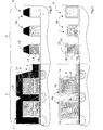
- a circuit structure integrated on a semiconductor substrate 1 comprising a first plurality of electronic devices 4, for example non volatile memory cells.
- Each of these electronic devices 4 comprises a region 4a projecting from the semiconductor substrate 1, formed for example by one or more conductive layers 7, 9 being electrically insulated from each other by means of an insulating layer 8.
- the region 4a is coated with a first sealing structure 17 of a first thickness performing the sealing of these electronic devices 4.
- this first sealing structure 17 comprises a plurality of insulating layers 14, 16.
- the first sealing structure 17 also covers a portion of the exposed semiconductor substrate 1 between the single electronic devices 4.
- the semiconductor substrate 1 also comprises a second plurality of electronic devices 5, for example traditional transistors.
- Each of these electronic devices 5 comprises a region 5a projecting from the semiconductor substrate 1, formed for example by at least one conductive layer 11.
- the region 5a is coated with a second sealing structure 18 performing the sealing of these electronic devices 5.
- the second sealing structure 18 has a lower thickness, on the semiconductor substrate 1, than the thickness of the first sealing structure 17 covering the electronic devices 4.
- the second sealing structure 18 has a lower thickness on the vertical walls of the region 5a, while it has a higher thickness on the top of this region 5a. It is thus possible to realise very close electronic devices 5 allowing a higher integration scale.
- the second sealing structure 18 comprises at least an insulating structure 16.
- a matrix 2 of cells with associated control circuitry 3 is realised on a semiconductor substrate 1, the cell matrix 2 comprising a plurality of non volatile memory cells 2, while the control circuitry 3 comprises a plurality of transistors 5.
- a manufacturing process of the cell matrix 2 provides the formation, on the semiconductor substrate 1 in cascade, of a first insulating layer 6, for example silicon oxide, a first conductive layer 7, for example polysilicon, a second insulating layer 8, for example silicon oxide, and a second conductive layer 9, for example polysilicon.
- a third insulating layer 10 for example silicon oxide, and a third conductive layer 11, for example polysilicon is instead provided to realise the circuitry.
- the third conductive layer 11 is realised simultaneously with the second conductive layer 9.
- the third insulating layer 10 is realised simultaneously with the second insulating layer 8.
- a first photoresist material layer 12 is then deposited on the whole semiconductor substrate 1.
- the first photoresist layer 12 is etched to define a plurality of gate regions 4a of the memory cells 4, while a portion of this first photoresist material layer 12 in the circuitry 3 is left to screen the third conductive layer 11, as shown in figure 1.
- the first photoresist material layer 12 is then removed and implants are carried out to realise, in a traditional way, source and drain regions 13 of the memory cell 4.
- these implants are optimised to improve the memory cell 4 performances.
- memory cells 4 are then sealed forming a first insulating or sealing layer 14, for example through a high-temperature fast oxidation step.
- the first sealing layer 14 is 3-7 nm thick, for example about 4 nm.
- the so-formed sealing layer 14 coats not only the gate regions 4a of memory cells 4, but it also covers a portion of the semiconductor substrate 1 being left exposed in the matrix 2, and the third conductive layer 11 not yet defined in the circuitry 3, as shown in figure 2.
- a second photoresist material layer 15 is then deposited on the whole semiconductor substrate 1.
- this second photoresist layer 15 is then etched to define a plurality of gate regions 5a of transistors 5, while a portion of this second photoresist material layer 15 on the matrix 2 is left to screen the memory cells 4 of the matrix 2, as shown in figure 3.
- circuitry portions being uncovered by the photoresist layer 15 undergo first an etching step to remove the first sealing layer 14 and then an etching step to remove the conductive layer 11.
- transistors 5 are sealed by forming a second thin insulating or sealing layer 16, for example through an oxidation step.
- this second thin sealing layer 16 is between 1 and 3 nm, for example 2 nm.
- this second thin sealing layer 16 completely covers the first sealing layer 14.
- a first sealing structure 17 is thus formed, comprising the first sealing layer 14 and the second sealing layer 16, which completely coats the gate regions 4a of memory cells 4 to perform the sealing step thereof.
- a second sealing structure 18 is formed, which completely coats the gate regions 5a of transistors 5 to seal them, this second sealing structure 18 comprising the second sealing layer 16 and portions of the first sealing layer 14 which are on the upper portion of the gate regions 5a of transistors 5.
- this second thin sealing layer 16 does not affect the electric capacities of cells 4, both because the source and drain regions 13 in the matrix 2 have already been formed, and because the heat treatments involved in the formation of this second thin sealing layer 16 are performed at lower temperatures than the temperatures undergone by the cells 4 for the specific sealing thereof.
- both traditional memory cells 4 and traditional transistors 5 can be successfully integrated on the common semiconductor substrate 1, penalising neither the performances nor the reliability, with the following differences with respect to prior art methods:
- the sealing layer 14 is then removed from the conductive layer 11, before defining real gate regions 5a in the circuitry 3.
- the second sealing structure 18 sealing the gate regions 5a of transistors 5 is only formed by the second sealing layer 16.
- This alternative embodiment is advantageously applied when the materials used to form the sealing layer 14 for sealing memory cells 4 are different from thermal oxide and must be necessarily removed to allow the conductive layer 11 to be correctly etched to define gate regions 5a in the circuitry 3.
- the method according to the invention allows typologies of electronic devices requiring different types of sealing to be integrated without jeopardising the individually optimised performances and reliability for each device, with low or no cost.
- the sealing step of these electronic devices is achieved by means of sealing layers with different thickness, and, in case, also comprising materials being formed immediately after defining the devices of the matrix 2 and of the circuitry 3.
Landscapes
- Engineering & Computer Science (AREA)
- Manufacturing & Machinery (AREA)
- Non-Volatile Memory (AREA)
- Metal-Oxide And Bipolar Metal-Oxide Semiconductor Integrated Circuits (AREA)
Priority Applications (5)
| Application Number | Priority Date | Filing Date | Title |
|---|---|---|---|
| DE60326351T DE60326351D1 (de) | 2003-10-22 | 2003-10-22 | Versiegelungsverfahren für auf einem gemeinsamen Substrat hergestellte elektronische Bauelemente |
| EP03425687A EP1526568B1 (de) | 2003-10-22 | 2003-10-22 | Versiegelungsverfahren für auf einem gemeinsamen Substrat hergestellte elektronische Bauelemente |
| US10/971,774 US7078294B2 (en) | 2003-10-22 | 2004-10-22 | Sealing method for electronic devices formed on a common semiconductor substrate and corresponding circuit structure |
| US11/457,948 US20070026610A1 (en) | 2003-10-22 | 2006-07-17 | Sealing method for electronic devices formed on a common semiconductor substrate and corresponding circuit structure |
| US11/457,966 US7410872B2 (en) | 2003-10-22 | 2006-07-17 | Sealing method for electronic devices formed on a common semiconductor substrate and corresponding circuit structure |
Applications Claiming Priority (1)
| Application Number | Priority Date | Filing Date | Title |
|---|---|---|---|
| EP03425687A EP1526568B1 (de) | 2003-10-22 | 2003-10-22 | Versiegelungsverfahren für auf einem gemeinsamen Substrat hergestellte elektronische Bauelemente |
Publications (2)
| Publication Number | Publication Date |
|---|---|
| EP1526568A1 true EP1526568A1 (de) | 2005-04-27 |
| EP1526568B1 EP1526568B1 (de) | 2009-02-25 |
Family
ID=34384746
Family Applications (1)
| Application Number | Title | Priority Date | Filing Date |
|---|---|---|---|
| EP03425687A Expired - Lifetime EP1526568B1 (de) | 2003-10-22 | 2003-10-22 | Versiegelungsverfahren für auf einem gemeinsamen Substrat hergestellte elektronische Bauelemente |
Country Status (3)
| Country | Link |
|---|---|
| US (2) | US7078294B2 (de) |
| EP (1) | EP1526568B1 (de) |
| DE (1) | DE60326351D1 (de) |
Families Citing this family (2)
| Publication number | Priority date | Publication date | Assignee | Title |
|---|---|---|---|---|
| US20070026610A1 (en) * | 2003-10-22 | 2007-02-01 | Stmicroelectronics S.R.L. | Sealing method for electronic devices formed on a common semiconductor substrate and corresponding circuit structure |
| US8692310B2 (en) | 2009-02-09 | 2014-04-08 | Spansion Llc | Gate fringing effect based channel formation for semiconductor device |
Citations (4)
| Publication number | Priority date | Publication date | Assignee | Title |
|---|---|---|---|---|
| JPH08153860A (ja) * | 1994-11-29 | 1996-06-11 | Mitsubishi Electric Corp | 半導体記憶装置及びその製造方法 |
| US6468867B1 (en) * | 2001-07-30 | 2002-10-22 | Macronix International Co., Ltd. | Method for forming the partial salicide |
| US20030151069A1 (en) * | 2001-12-25 | 2003-08-14 | Kikuko Sugimae | Semiconductor device and manufacturing method |
| US6630378B1 (en) * | 1996-03-27 | 2003-10-07 | Nec Electronics Corporation | Method of fabricating a dynamic random access memory device having stacked capacitor memory cell arrays |
Family Cites Families (2)
| Publication number | Priority date | Publication date | Assignee | Title |
|---|---|---|---|---|
| US6798002B1 (en) * | 1999-10-13 | 2004-09-28 | Advanced Micro Devices, Inc. | Dual-purpose anti-reflective coating and spacer for flash memory and other dual gate technologies and method of forming |
| JP4057770B2 (ja) * | 2000-10-11 | 2008-03-05 | 株式会社ルネサステクノロジ | 半導体集積回路装置 |
-
2003
- 2003-10-22 DE DE60326351T patent/DE60326351D1/de not_active Expired - Lifetime
- 2003-10-22 EP EP03425687A patent/EP1526568B1/de not_active Expired - Lifetime
-
2004
- 2004-10-22 US US10/971,774 patent/US7078294B2/en not_active Expired - Lifetime
-
2006
- 2006-07-17 US US11/457,966 patent/US7410872B2/en not_active Expired - Lifetime
Patent Citations (4)
| Publication number | Priority date | Publication date | Assignee | Title |
|---|---|---|---|---|
| JPH08153860A (ja) * | 1994-11-29 | 1996-06-11 | Mitsubishi Electric Corp | 半導体記憶装置及びその製造方法 |
| US6630378B1 (en) * | 1996-03-27 | 2003-10-07 | Nec Electronics Corporation | Method of fabricating a dynamic random access memory device having stacked capacitor memory cell arrays |
| US6468867B1 (en) * | 2001-07-30 | 2002-10-22 | Macronix International Co., Ltd. | Method for forming the partial salicide |
| US20030151069A1 (en) * | 2001-12-25 | 2003-08-14 | Kikuko Sugimae | Semiconductor device and manufacturing method |
Non-Patent Citations (1)
| Title |
|---|
| PATENT ABSTRACTS OF JAPAN vol. 1996, no. 10 31 October 1996 (1996-10-31) * |
Also Published As
| Publication number | Publication date |
|---|---|
| US7078294B2 (en) | 2006-07-18 |
| US7410872B2 (en) | 2008-08-12 |
| US20050112905A1 (en) | 2005-05-26 |
| EP1526568B1 (de) | 2009-02-25 |
| DE60326351D1 (de) | 2009-04-09 |
| US20070026576A1 (en) | 2007-02-01 |
Similar Documents
| Publication | Publication Date | Title |
|---|---|---|
| US20020185738A1 (en) | Integrated circuit having a passive device integrally formed therein | |
| US20020197788A1 (en) | Integrated circuit memory devices having non-volatile memory transistors and methods of fabricating the same | |
| KR0146401B1 (ko) | 스택 게이트 구조를 갖고 있는 반도체 집적 회로 장치의 제조 방법 | |
| JPH04302472A (ja) | 半導体装置およびその製造方法 | |
| KR20070055729A (ko) | 더미 게이트를 구비하는 반도체 소자의 구조 및 그 제조방법 | |
| JPH0964208A (ja) | 不揮発性半導体記憶装置およびその製造方法 | |
| EP1526568B1 (de) | Versiegelungsverfahren für auf einem gemeinsamen Substrat hergestellte elektronische Bauelemente | |
| US6812098B2 (en) | Method for manufacturing non-volatile memory device | |
| US7910444B2 (en) | Process for forming differential spaces in electronics device integrated on a semiconductor substrate | |
| US20070026610A1 (en) | Sealing method for electronic devices formed on a common semiconductor substrate and corresponding circuit structure | |
| US7582526B2 (en) | Method for manufacturing semiconductor device | |
| KR100568424B1 (ko) | 반도체 소자의 선택적 실리사이드 형성 방법 | |
| US20080057682A1 (en) | Manufacturing method of an integrated circuit formed on a semiconductor substrate | |
| JPH02201968A (ja) | 半導体装置の製造方法 | |
| KR100575361B1 (ko) | 플래시 게이트 및 고전압 게이트 형성 방법 | |
| KR0142602B1 (ko) | 플래쉬 이이피롬 소자의 제조방법 | |
| EP1770772B1 (de) | Verfahren zur Herstellung einer nichtflüchtigen Speichervorrichtung | |
| EP1677348B1 (de) | Verfahren zur Herstellung von nichtflüchtigen Speicherzellen und Peripherietransistoren | |
| KR100255159B1 (ko) | 플래쉬 이이피롬 셀 어레이의 소오스 라인 세그먼트 트랜지스터 제조 방법 | |
| KR20000044855A (ko) | 플래쉬 메모리 소자의 제조 방법 | |
| KR0147869B1 (ko) | 반도체 장치의 제조방법 | |
| KR19990060867A (ko) | 스텍 게이트 형성 방법 | |
| KR100744003B1 (ko) | 반도체 소자의 금속배선 형성방법 | |
| KR100260635B1 (ko) | Eprom 소자 제조방법 | |
| JP3783240B2 (ja) | フラッシュメモリの製造方法 |
Legal Events
| Date | Code | Title | Description |
|---|---|---|---|
| PUAI | Public reference made under article 153(3) epc to a published international application that has entered the european phase |
Free format text: ORIGINAL CODE: 0009012 |
|
| AK | Designated contracting states |
Kind code of ref document: A1 Designated state(s): AT BE BG CH CY CZ DE DK EE ES FI FR GB GR HU IE IT LI LU MC NL PT RO SE SI SK TR |
|
| AX | Request for extension of the european patent |
Extension state: AL LT LV MK |
|
| 17P | Request for examination filed |
Effective date: 20051026 |
|
| AKX | Designation fees paid |
Designated state(s): DE FR GB IT |
|
| 17Q | First examination report despatched |
Effective date: 20070215 |
|
| GRAP | Despatch of communication of intention to grant a patent |
Free format text: ORIGINAL CODE: EPIDOSNIGR1 |
|
| RTI1 | Title (correction) |
Free format text: SEALING METHOD FOR ELECTRONIC DEVICES FORMED ON A COMMON SEMICONDUCTOR SUBSTRATE |
|
| GRAS | Grant fee paid |
Free format text: ORIGINAL CODE: EPIDOSNIGR3 |
|
| GRAA | (expected) grant |
Free format text: ORIGINAL CODE: 0009210 |
|
| AK | Designated contracting states |
Kind code of ref document: B1 Designated state(s): DE FR GB IT |
|
| REG | Reference to a national code |
Ref country code: GB Ref legal event code: FG4D |
|
| REF | Corresponds to: |
Ref document number: 60326351 Country of ref document: DE Date of ref document: 20090409 Kind code of ref document: P |
|
| PLBE | No opposition filed within time limit |
Free format text: ORIGINAL CODE: 0009261 |
|
| STAA | Information on the status of an ep patent application or granted ep patent |
Free format text: STATUS: NO OPPOSITION FILED WITHIN TIME LIMIT |
|
| 26N | No opposition filed |
Effective date: 20091126 |
|
| REG | Reference to a national code |
Ref country code: FR Ref legal event code: ST Effective date: 20100630 |
|
| PG25 | Lapsed in a contracting state [announced via postgrant information from national office to epo] |
Ref country code: FR Free format text: LAPSE BECAUSE OF NON-PAYMENT OF DUE FEES Effective date: 20091102 |
|
| PG25 | Lapsed in a contracting state [announced via postgrant information from national office to epo] |
Ref country code: GB Free format text: LAPSE BECAUSE OF NON-PAYMENT OF DUE FEES Effective date: 20091022 |
|
| PG25 | Lapsed in a contracting state [announced via postgrant information from national office to epo] |
Ref country code: IT Free format text: LAPSE BECAUSE OF FAILURE TO SUBMIT A TRANSLATION OF THE DESCRIPTION OR TO PAY THE FEE WITHIN THE PRESCRIBED TIME-LIMIT Effective date: 20090225 |
|
| REG | Reference to a national code |
Ref country code: DE Ref legal event code: R082 Ref document number: 60326351 Country of ref document: DE Representative=s name: SAMSON & PARTNER, PATENTANWAELTE, DE |
|
| REG | Reference to a national code |
Ref country code: DE Ref legal event code: R081 Ref document number: 60326351 Country of ref document: DE Owner name: MICRON TECHNOLOGY, INC., US Free format text: FORMER OWNER: STMICROELECTRONICS S.R.L., AGRATE BRIANZA, IT Effective date: 20130515 Ref country code: DE Ref legal event code: R082 Ref document number: 60326351 Country of ref document: DE Representative=s name: SAMSON & PARTNER, PATENTANWAELTE, DE Effective date: 20130515 Ref country code: DE Ref legal event code: R081 Ref document number: 60326351 Country of ref document: DE Owner name: MICRON TECHNOLOGY, INC., BOISE, US Free format text: FORMER OWNER: STMICROELECTRONICS S.R.L., AGRATE BRIANZA, MAILAND/MILANO, IT Effective date: 20130515 Ref country code: DE Ref legal event code: R082 Ref document number: 60326351 Country of ref document: DE Representative=s name: SAMSON & PARTNER PATENTANWAELTE MBB, DE Effective date: 20130515 Ref country code: DE Ref legal event code: R081 Ref document number: 60326351 Country of ref document: DE Owner name: MICRON TECHNOLOGY, INC., BOISE, US Free format text: FORMER OWNER: STMICROELECTRONICS S.R.L., AGRATE BRIANZA, IT Effective date: 20130515 |
|
| REG | Reference to a national code |
Ref country code: DE Ref legal event code: R079 Ref document number: 60326351 Country of ref document: DE Free format text: PREVIOUS MAIN CLASS: H01L0021824700 Ipc: H01L0027115000 |
|
| REG | Reference to a national code |
Ref country code: DE Ref legal event code: R079 Ref document number: 60326351 Country of ref document: DE Free format text: PREVIOUS MAIN CLASS: H01L0027115000 Ipc: H10B0069000000 |
|
| PGFP | Annual fee paid to national office [announced via postgrant information from national office to epo] |
Ref country code: DE Payment date: 20220527 Year of fee payment: 20 |
|
| REG | Reference to a national code |
Ref country code: DE Ref legal event code: R071 Ref document number: 60326351 Country of ref document: DE |