EP1526535A2 - Verfahren und System zur Benutzung einer optischen Sensoranordnung zur Steuerung einer Etikettierungsvorrichtung - Google Patents
Verfahren und System zur Benutzung einer optischen Sensoranordnung zur Steuerung einer Etikettierungsvorrichtung Download PDFInfo
- Publication number
- EP1526535A2 EP1526535A2 EP04256084A EP04256084A EP1526535A2 EP 1526535 A2 EP1526535 A2 EP 1526535A2 EP 04256084 A EP04256084 A EP 04256084A EP 04256084 A EP04256084 A EP 04256084A EP 1526535 A2 EP1526535 A2 EP 1526535A2
- Authority
- EP
- European Patent Office
- Prior art keywords
- sensor array
- optical sensor
- optical
- imageable
- texture
- Prior art date
- Legal status (The legal status is an assumption and is not a legal conclusion. Google has not performed a legal analysis and makes no representation as to the accuracy of the status listed.)
- Withdrawn
Links
- 230000003287 optical effect Effects 0.000 title claims abstract description 207
- 238000002372 labelling Methods 0.000 title claims abstract description 32
- 238000000034 method Methods 0.000 title claims abstract description 26
- 230000004044 response Effects 0.000 claims abstract description 9
- 238000007639 printing Methods 0.000 claims description 5
- 238000006073 displacement reaction Methods 0.000 claims description 2
- 238000004891 communication Methods 0.000 description 8
- 238000009304 pastoral farming Methods 0.000 description 5
- 239000000853 adhesive Substances 0.000 description 4
- 230000001070 adhesive effect Effects 0.000 description 4
- 230000008859 change Effects 0.000 description 4
- 238000010586 diagram Methods 0.000 description 4
- 238000013461 design Methods 0.000 description 3
- 238000005516 engineering process Methods 0.000 description 3
- 238000009987 spinning Methods 0.000 description 3
- 230000001427 coherent effect Effects 0.000 description 2
- 238000013500 data storage Methods 0.000 description 2
- 230000003993 interaction Effects 0.000 description 2
- 230000008569 process Effects 0.000 description 2
- 238000012545 processing Methods 0.000 description 2
- 238000003491 array Methods 0.000 description 1
- 230000000295 complement effect Effects 0.000 description 1
- 230000001143 conditioned effect Effects 0.000 description 1
- 230000008878 coupling Effects 0.000 description 1
- 238000010168 coupling process Methods 0.000 description 1
- 238000005859 coupling reaction Methods 0.000 description 1
- 230000003247 decreasing effect Effects 0.000 description 1
- 230000001419 dependent effect Effects 0.000 description 1
- 230000002708 enhancing effect Effects 0.000 description 1
- 239000004744 fabric Substances 0.000 description 1
- 239000000835 fiber Substances 0.000 description 1
- 238000010304 firing Methods 0.000 description 1
- 238000005286 illumination Methods 0.000 description 1
- 239000003550 marker Substances 0.000 description 1
- 239000000463 material Substances 0.000 description 1
- 238000005259 measurement Methods 0.000 description 1
- 238000012986 modification Methods 0.000 description 1
- 230000004048 modification Effects 0.000 description 1
- 230000000737 periodic effect Effects 0.000 description 1
- 230000005855 radiation Effects 0.000 description 1
- 230000003595 spectral effect Effects 0.000 description 1
- 230000000007 visual effect Effects 0.000 description 1
Images


Classifications
-
- G—PHYSICS
- G11—INFORMATION STORAGE
- G11B—INFORMATION STORAGE BASED ON RELATIVE MOVEMENT BETWEEN RECORD CARRIER AND TRANSDUCER
- G11B23/00—Record carriers not specific to the method of recording or reproducing; Accessories, e.g. containers, specially adapted for co-operation with the recording or reproducing apparatus ; Intermediate mediums; Apparatus or processes specially adapted for their manufacture
- G11B23/38—Visual features other than those contained in record tracks or represented by sprocket holes the visual signals being auxiliary signals
- G11B23/40—Identifying or analogous means applied to or incorporated in the record carrier and not intended for visual display simultaneously with the playing-back of the record carrier, e.g. label, leader, photograph
-
- B—PERFORMING OPERATIONS; TRANSPORTING
- B65—CONVEYING; PACKING; STORING; HANDLING THIN OR FILAMENTARY MATERIAL
- B65C—LABELLING OR TAGGING MACHINES, APPARATUS, OR PROCESSES
- B65C9/00—Details of labelling machines or apparatus
- B65C9/26—Devices for applying labels
-
- B—PERFORMING OPERATIONS; TRANSPORTING
- B41—PRINTING; LINING MACHINES; TYPEWRITERS; STAMPS
- B41J—TYPEWRITERS; SELECTIVE PRINTING MECHANISMS, i.e. MECHANISMS PRINTING OTHERWISE THAN FROM A FORME; CORRECTION OF TYPOGRAPHICAL ERRORS
- B41J11/00—Devices or arrangements of selective printing mechanisms, e.g. ink-jet printers or thermal printers, for supporting or handling copy material in sheet or web form
- B41J11/009—Detecting type of paper, e.g. by automatic reading of a code that is printed on a paper package or on a paper roll or by sensing the grade of translucency of the paper
-
- B—PERFORMING OPERATIONS; TRANSPORTING
- B41—PRINTING; LINING MACHINES; TYPEWRITERS; STAMPS
- B41J—TYPEWRITERS; SELECTIVE PRINTING MECHANISMS, i.e. MECHANISMS PRINTING OTHERWISE THAN FROM A FORME; CORRECTION OF TYPOGRAPHICAL ERRORS
- B41J3/00—Typewriters or selective printing or marking mechanisms characterised by the purpose for which they are constructed
- B41J3/407—Typewriters or selective printing or marking mechanisms characterised by the purpose for which they are constructed for marking on special material
- B41J3/4071—Printing on disk-shaped media, e.g. CDs
-
- G—PHYSICS
- G11—INFORMATION STORAGE
- G11B—INFORMATION STORAGE BASED ON RELATIVE MOVEMENT BETWEEN RECORD CARRIER AND TRANSDUCER
- G11B7/00—Recording or reproducing by optical means, e.g. recording using a thermal beam of optical radiation by modifying optical properties or the physical structure, reproducing using an optical beam at lower power by sensing optical properties; Record carriers therefor
- G11B7/002—Recording, reproducing or erasing systems characterised by the shape or form of the carrier
- G11B7/0037—Recording, reproducing or erasing systems characterised by the shape or form of the carrier with discs
Definitions
- Optical discs have fast become an industry standard for data storage in the fields of computers, video, and music.
- Optical discs include, but are not limited to, compact discs (CDs), Digital Video (or Versatile) Discs (DVDs), and game system discs in a variety of formats.
- Commercially produced optical discs usually have digital data recorded on one side of the disc and a visual display printed on the opposite side of the disc.
- optical discs are created that can store data on both sides of the disc. However, in most cases, it is desirable to limit the optical disc data to a single side of the disc, leaving the other side of the disc for printed text, patterns, or graphics.
- the printed labeling on a non-data side of an optical disc can include a decorative design, text identifying the data stored on the disc, or both.
- a method for using an optical sensor array to control a labeling device includes scanning a surface texture of an imageable media with the optical sensor array, collecting surface data corresponding to the surface texture of the imageable media, and controlling the labeling device in response to the surface data.
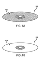
- Figs. 1A and 1B illustrate perspective views of an optical disc according to one exemplary embodiment.
- Fig. 2 is a block diagram of an optical disc drive according to one exemplary embodiment.
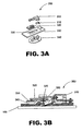
- Fig. 3A is an exploded view of the components of an optical sensor array according to one exemplary embodiment.
- Fig. 3B is an assembled view of an optical sensor array according to one exemplary embodiment.
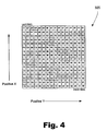
- Fig. 4 illustrates a photodetector array according to one exemplary embodiment.
- Figs. 5A and 5B illustrate the components of an optical sensor array according to one exemplary embodiment.
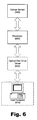
- Fig. 6 is a block diagram illustrating the communication path between an optical sensor array and a host computer according to one exemplary embodiment.
- Fig. 7 is a flow chart illustrating the process of controlling an optical disc drive according to one exemplary embodiment.
- Fig. 8 is a block diagram of an optical disc with an optical sensor array mounted beneath the optical disc according to one exemplary embodiment.
- Fig. 9 is a block diagram of an optical disc with an optical sensor array mounted above the optical disc according to one exemplary embodiment.
- Fig. 10 is an assembled view of a manually controlled labeling device including an optical sensor array according to one exemplary embodiment.
- the present specification describes a method and a system for controlling an optical disc drive based on information received from an optical sensor array.
- the optical sensor array may provide information including, but in no way limited to, the position of an optical disc drive moveable member, rotational speed of an optical disc, and/or information regarding previously printed disc information.
- optical disk is meant to be understood as any data storage disk capable of containing optically readable information including, but in no way limited to, compact discs (CDs), Digital Video (or Versatile) Discs (DVDs), or game system discs in a variety of formats.
- CDs compact discs
- DVDs Digital Video (or Versatile) Discs
- game system discs in a variety of formats.
- an angle of incidence is meant to be understood as an angle between an incident ray of light and the perpendicular to a surface.
- imageable medium is meant to be understood as any material whose lucidity may be selectively varied with the application of photonic radiation
- FIG. 1A and Fig. 1B illustrate perspective views of an optical disk according to one exemplary embodiment.
- an optical disc (100) is typically a round wafer of imageable medium with two planar surfaces.
- one planar surface of the disc is used for storing digital data (114; Fig. 1B) and the opposite side of the disc is used for some type of printed labeling (102; Fig. 1A).
- both sides of the optical disc (100) may be used for storing digital data.
- the printed labeling on the non-data side of the disc may include a decorative design, text identifying the data stored on the disc, or both.
- the printed labeling (102) may be affixed to the optical disc (100) in a variety of manners.
- the label may be printed on a printing device and then affixed to the optical disc (100) with some type of adhesive.
- the label may be written directly onto the disc (100) using a photonic emitter of an optical disc drive.
- a number of optical disks (100) include one or more surfaces whose optical characteristics may be modified by the selective application of a photonic emitter such as a laser from an optical disk drive.
- a photonic emitter such as a laser from an optical disk drive.
- the lucidity of the disk surface is modified. This change in lucidity may then be used to form patterns or labels on the surface of the disk (100). While this method of labeling disk surfaces is advantageous, traditional optical disk drives are unable to both detect previously formed labels or to identify various locations with respect to the optical disk.
- an optical disc drive it is desirable to operate an optical disc drive at a relatively low rotational speed.
- stepper and direct current (DC) motors are limited as to how precisely they can track the position of the sled.
- the data side of an optical disc is faintly marked with guides to aid an optical pickup unit (OPU) in determining its position.
- OPU optical pickup unit
- the non-data or label side of the optical disc is usually unmarked, thus causing a potential problem for those who wish to write a label on the unmarked non-data side of the disc due to an inability to track the position of the sled.
- Fig. 2 illustrates some of the components of an optical disc drive (200) according to one exemplary embodiment.
- an optical disc drive (200) such as the one illustrated in Fig. 2 is typically used to read data from an optical disc (100; Fig. 1A). Data may be read from an optical disk by first spinning the optical disc (100; Fig. 1A) on a spindle (201) controlled by a motor (not shown). While the optical disc (100) is spinning, laser light is focused onto the disc (100; Fig. 1A) using a lens (205) and, upon reflecting off the optical disc (100; Fig. 1A), the light is sensed using a photodetector.
- the laser, the laser driver, the lens, and the photodetector comprise an optical pickup unit (OPU).
- OPU optical pickup unit
- the OPU is disposed on a sled (206) which is actuated up or down a sled support rail (203) by a stepper or DC motor (not shown) which is covered by a motor housing (211) and coupled with a gearing system (210).
- the laser and photodetector are able to "read" the disc (100; Fig. 1A) by detecting bumps and grooves imprinted on the disc (100; Fig. 1A).
- the sled is held in place by a sled retainer (207) as the sled moves along the guide rail (208).
- the data read by the optical disc drive (200) may be transferred via a flex cable (202) to a communicatively coupled computing device (not shown).
- the entire assembly of the above-mentioned parts may be housed in an optical device drive chassis (204) and securely fastened using a number of mounts (209).
- the OPU illustrated in Fig. 2 may also be coupled to an optical sensor configured to scan and provide information regarding the surface texture of any disk (100; Fig. 1A) being scanned.
- the optical sensor may be affixed to a sled, on which the optical pickup unit (OPU) typically resides. When attached next to the OPU on the sled, the optical sensor travels with the sled. The optical sensor is then capable of detecting where the sled is in reference to the optical disc. This process will be explained in greater detail below.
- Fig. 3A is an exploded view illustrating the components of an exemplary optical sensor array (350) that may be coupled to the OPU as explained above.
- the exemplary optical sensor array (350) may include a positioning clip (300), an illuminator (310), a photo sensor (320) containing a photo sensor array (325; Fig. 3B), a printed circuit board (330) containing a center orifice (335), and a lens (340).
- the illuminator (310) illustrated in Fig. 3A may be any light source, coherent or non-coherent, capable of illuminating a surface of a disk (100; Fig. 1A) such that the photodetector array (325; Fig. 3B) may sense changes in the surface texture. Changes in surface texture that may be illuminated by the present illuminator (310) and subsequently detected by the photodetector array (325; Fig 3B) may include, but are in no way limited to, surface imperfections, prior labels, or any other surface characteristics.
- the illuminator may include, but is in no way limited to one or more light emitting diodes (LEDs) including integrated or separate projection optics, one or more lasers, or cavity resonant light emitting diodes.
- the projection optics may include diffractive optic elements that homogenize the light emitted by the illuminator (310).
- Choice of characteristics such as wavelength of the light being emitted by the illuminator (310) is dependent upon the surface being illuminated, the surface features being imaged, and the response of the photodetector array (325; Fig. 2B).
- the emitted light may be visible, infrared, ultraviolet, narrow band, or broadband.
- a shorter wavelength might be used for exciting a phosphorescing or fluorescing emission from a surface thereby enhancing the sensing of surface texture changes.
- the wavelength may also be selectively chosen if the surface exhibits significant spectral dependence that can provide images having high contrast.
- the light may either be collimated or non-collimated.
- Collimated light may be used for grazing illumination in that it provides good contrast in surface textures that derive from surface profile geometry (e.g., bumps, grooves) and surface structural elements (e.g., fibers comprising the surfaces of papers, fabrics, woods, etc.).
- surface profile geometry e.g., bumps, grooves
- surface structural elements e.g., fibers comprising the surfaces of papers, fabrics, woods, etc.
- the lens (340) illustrated in Fig. 3A may be any optical device capable of directing and focusing the light emitted from the illuminator (310) onto an optical disc or other desirable surface (100; Fig. 1A).
- the lens (340) may also be implemented to focus light from all or part of an illuminated area onto the photodetector array (325; Fig. 3B).
- the photodetector (320) containing a photodetector array (325; Fig. 3B) is an optical sensor that may be used to implement a surface scanning device.
- the photodetector (320) may also include a digital signal processor (not shown) for processing the digital signals generated by the photodetector array (325; Fig. 3B), a communication channel such as a two channel quadrature output and a two wire serial port for outputting the ⁇ X and ⁇ Y relative displacement values that are converted into two channel quadrature signals by the digital signal processor.
- the photodetector array (325) may include a number of pixels (00-FF), of the same or varying size, that are spaced at regular intervals.
- the pixels (00-FF) may not be configured to discern individual features of the object being monitored; rather, each pixel may effectively measure an intensity level of a portion of an image or projection of a surface feature within its field of view.
- the pixels (00-FF) that make up the photodetector array (325) are configured to generate output signals indicative of the contrast variations of the imaged surface features and texture.
- the pixels (00-FF) of the photodetector array (325) typically detect different intensity levels due to random size, shape, and distribution of surface features and texture as well as a randomness of the scattering of light by the surface features and texture.
- the object being monitored such as an optical disk (100; Fig. 1A)
- different features of the object's surface will come into view of the pixels (00-FF) and the intensity levels sensed by the pixels (00-FF) will change. This change in intensity levels may then be equated with a relative motion of the optical sensor array. Additionally, the change in intensity levels can be equated with a label or other marking on the surface of the optical disk (100; Fig. 1A).
- photodetector array (325) illustrated in Fig. 3 is shown as a 16 x 16 array, the photodetector array may be comprised of any number of pixels.
- FIG. 3B an assembled optical sensor array (350) that may be coupled to the OPU is illustrated.
- the illuminator (310) and the lens (340) are coupled to a printed circuit board (330).
- the lens (340) includes a top portion that extends upward through a center orifice (335; Fig. 3A) of the printed circuit board (330) while the illuminator (310) is communicatively coupled to the top portion of the printed circuit board (330).
- the photodetector (320) may then be disposed on top of the lens (340) and communicatively coupled to the printed circuit board (330) such that the photodetector array (325) is in optical communication with the lens (340) and any optical disc surface (100) that passes under it.
- the positioning clip may then be secured over the photodetector (320) and the illuminator (310).
- the positioning clip (300) securely couples the illuminator (310) protecting it from damage as well as positioning the illuminator (310) in optical communication with the lens (340).
- the positioning clip (300) also secures the photodetector (320) onto the lens (340) such that the photodetector array (325) is in optical communication with the lens (340) and with the center orifice (335) of the printed circuit board (330).
- the assembled optical sensor (350) is then coupled to the optical device drive sled (206; Fig. 2).
- Fig. 5A illustrates an exploded view of the interaction that may occur between the structural components of the present optical sensor array (350) according to one exemplary embodiment.
- the present optical sensor array (350) is incorporated to measure the surface features or texture and the rotation R of an object (180) such as an optical disc (100, Fig. 1A)
- the illuminator (310) is positioned such that any light emitted by the illuminator (310) will strike the object (180) at a target area (500).
- the illuminator (310) is positioned relative to the object (180), such that light emitted from the illuminator (310) will strike the target area (500) at a pre-determined grazing angle ⁇ thereby illuminating the target area (500) of the object optically coupling the photodetector (320) to the target area (500).
- the grazing angle ⁇ is the complementary angle of the angle of incidence.
- the light grazing the object (180) is scattered by the random natural surface features of the surface texture producing a high number of domains of lightness and darkness. The domains of lightness and darkness are focused from the target area to the photodetector (320) through the lens (340).
- the photodetector array (325) located on the photodetector (320) may then receive and record the domains of lightness and darkness. As the object (180) is rotated R and subsequent domain information is collected, the changing domains of lightness and darkness produced by the changing surface features may be compared to determine relative motion of the object (180). As shown in Fig. 5A, the target area (500) of the present optical sensor array (350) can be much larger than the typical area that may be scanned by a laser. This allows the present optical sensor array (350) to gather marking information much more quickly than using the laser and photodetector on the OPU.
- Fig. 5B illustrates the interaction between components of the present optical sensor array (350) when measuring the linear motion of an optical device sled (206, Fig. 2) in relation to an optical disc (cross-section shown) (100).
- the illuminator (310) is situated at a grazing angle ⁇ , such that the photodetector (320) may be in optical communication with a specified target area (500) of the optical disc (100).
- the photodetector array (325) collects data corresponding to domains of lightness and darkness illuminated by light emitted by the illuminator (310) through the lens (340). Periodic differences in the lightness and darkness of the collected domains may be used to identify relative motion between the optical disc (100) and the photodetector (320). Further details regarding optical measurement technology may be found in U.S. Patent No. 6,246,050, which is incorporated herein by reference.
- Fig. 6 illustrates an exemplary line of communication between an optical sensor array (350) and a host computer (610).
- the optical sensor array (350) may be communicatively connected with an optical disc drive processor (820) as shown in Fig. 6.
- the optical sensor array (350) sends information to the processor (820) which, in turn, controls the functions of the optical disc drive (200; Fig. 2).
- An optical disc drive driver (600) is associated with the processor (820) and acts as an interface between the host computer (610) and the processor (820).
- a user may control the optical disc drive (200) and each of the drive's functions by programming the optical disc drive driver (600). For example, the user may want the optical disc drive sled (808; Fig.
- optical disc drive (200; Fig. 2) may be used to decrease the rotational speed of the disc (100; Fig. 8) if previously printed disc information is found on the disk surface (102; Fig. 8). Any of these functions may be controllably changed by editing the optical disc drive driver (600).
- Fig. 7 illustrates a flowchart demonstrating how an optical sensor array (350, Fig. 3A) can be used to provide information for controlling the optical disc drive (200, Fig. 2).
- the optical sensor array (350; Fig. 3A) is physically mounted on the OPU drive sled (step 700) and electronically coupled to the OPU drive (step 701). It will be understood that steps 700 and 701 may be omitted if the optical sensor array (350; Fig. 8) has already been installed in and electronically coupled to the optical disc drive (200; Fig. 2).
- the user may load the optical disk (100; Fig. 1A) into the optical disk drive (step 702). Once loaded, the optical sensor array (350; Fig.
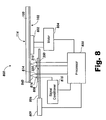
- Fig. 8 illustrates an optical disc drive assembly (800) that may be used to perform the method illustrated in Fig. 7.
- the optical disc drive assembly (800) illustrated in Fig. 8 includes a spindle (802) and a motor (804) for holding and spinning the optical disc (100).
- the label side (102) of the disc (100) is shown facing the spindle (802) such that a label may be written to the disc (100). It will be understood, of course, that data may also be written to the data side (114) of the optical disc (100) if the disc is turned over.
- a focused energy emitting device which in the present embodiment includes a laser (814), is disposed on the sled (808).
- the laser (814) may be used to read and/or write to the optical disc (100) by emitting a beam (840) that is reflected and read by a photodetector (816) that is also positioned on the sled (808).
- the laser (814) is used when reading data from the data side (114) of the optical disc (or, in some cases, when reading some data from the label side (102)). Signals received by the detector may be conditioned by a signal conditioner (815) when the system (800) is in a reading mode.
- the system (800) may be in a writing mode as shown in Fig. 8 and as the optical disc (100) spins, a label may be written on the label side (102) by applying a photonic beam (840) from the laser (814) or other photonic emitter at selective locations.
- the system is controlled by a processor (820).
- the processor may include, but is in no way limited to, a microprocessor, a microcontroller, a digital signal processor, etc.
- the processor (820) controls the firing of the laser (814) or other photonic emitter, the speed of the motor (804) (and thus the rotational speed of the optical disc (100)), and the position of the sled (808). Additionally, the processor (820) controls the optical sensor array assembly (350).
- the optical sensor array assembly (350) includes a light source (310), which is an LED in the present embodiment, and photodetector array (325).
- the optical sensor array assembly (350) is communicatively connected to the processor (820), thus enabling the optical sensor array (350) to send information to the processor (820).
- the optical sensor array (350) may be coupled to the optical disc drive sled (808) underneath the optical disc (100).
- the optical sensor array (350) may be affixed to a separate sled (808) held in place by guide rails (208; Fig. 2) above or below the optical disc (100).
- the optical sensor array (350) may be coupled to the optical disk drive sled (808) with screws, clips, adhesive, or any other type of fastener.
- the optical sensor array (350) is also electrically coupled to the optical disc drive (step 701; Fig. 7). Two-way communication is thus enabled between the optical sensor array (350) and the optical disc drive. Once an optical disc (100) is loaded in the system (800), the optical sensor array (350) may begin providing information for controlling the present system.
- either the data surface (114) or the non-data surface (102) of the optical disc (100) may be scanned (step 703; Fig. 7).
- the surface of the disk that is scanned depends on the number and location of optical sensor arrays (350) used as well as whether the disc is inserted data side (114) up or label side (102) up.
- information is collected and sent from the optical sensor array (350) to the optical disc drive processor (820).
- the optical sensor array (350) is capable of providing information regarding the sled (808) position, spindle (802) speed (rotational speed), and printed disc information which refers to how much (if any) of the non-data, label side (102) has been written to. This information will be collected by the optical sensor array (350) scanning surface textures as explained above. The information may then be used to control one or more optical disc drive functions. For example, based on the information received, the sled (808) may be moved up or down the track (806), the rotational speed of the spindle (802) may be increased or decreased, or the labeling or data on the optical disc (100) may be appended to.
- a sled (808) will have a "home” position from which the sled (808) can determine its position on the guide rail (208, Fig. 2).
- the sled (808) orients itself to the "home” position and advances along the track (806) to the position dictated by the optical disc drive driver (600, Fig. 6).
- the optical sensor array (350) may send coordinates to the processor (820) indicating how far the sled (808) has moved in either or both the X and Y directions and thus the current position of the sled (step 705; Fig. 7) may be rapidly determined.
- Such information may be updated thousands of times per second or more depending on the type of optical sensor (350) used.
- the optical sensor (350) is potentially capable of detecting very small movements due to the frequent updates.
- the processor (820) may determine the rotational speed of the disk (100) from the frequently updated coordinates provided by the optical sensor (350). Based on the rotational speed, the driver of the optical disc drive (800) can then step the spindle motor up or down to the desired rotational speed (step 706; Fig. 7).
- some applications may require a scan of the non-data side (114) of an optical disc (100) to determine if anything has been printed thereon, and if so, which parts of the disc contain printed disc information.
- printed disc information may include any type of labeling such as a decorative design, text identifying the data stored on the disc, or data of any type stored on or affixed to the optical disc (100).
- a label or data may be appended to the existing printed disc information, if present.
- the optical sensor array (350) moves along the track (806) the images taken by the optical sensor array (350) may be sent to the processor (820) for processing to determine where labeling or data begins and ends (step 707; Fig. 7). This information may be used to determine where the label or data may be appended or it may indicate to the user that nothing has been printed on that side of the disc (100).
- an optical sensor array assembly (350) may additionally or alternatively be positioned over the optical disc (100).
- the optical disc (100) can be tracked and/or scanned from above while the laser (814) and photodetector (816) mounted on the sled (808) remain and function below the optical disc (100).
- Figure 10 illustrates an assembled view of a manually controlled labeling device (1000) including an optical sensor array assembly (350) according to one exemplary embodiment.
- the manually controlled labeling device (1000) includes all of the above-mentioned components of a photosensor array assembly (350; Fig. 3). Additionally, the photosensor array assembly (350; Fig. 3) may be coupled to a photonic emitter.
- a user may translate the labeling device (1000) across a surface of an imageable medium (100) by hand (1010) or by any other device.
- the photosensor array may then analyze the texture of the imageable medium's surface to track the movement of the labeling device (1000), to analyze the surface characteristics of the imageable medium (100), or to control the labeling of the imageable medium (100).
- the present system and method provides for the use of an optical sensor array to control the function of a labeling device.
- the present system may analyze and control the position of system components, evaluate relative velocities of both imageable media and system components, and enhance the labeling of imageable media by the labeling device. This ability to evaluate and control velocities and positions increases the resolution of the labeling device due to dead reckoning of the surface and eliminates the need for additional components such as motor speed controls.
Landscapes
- Optical Recording Or Reproduction (AREA)
- Length Measuring Devices By Optical Means (AREA)
Applications Claiming Priority (2)
| Application Number | Priority Date | Filing Date | Title |
|---|---|---|---|
| US683021 | 2003-10-09 | ||
| US10/683,021 US7483184B2 (en) | 2003-10-09 | 2003-10-09 | Method and system for using an optical sensor array to control a labeling device |
Publications (2)
| Publication Number | Publication Date |
|---|---|
| EP1526535A2 true EP1526535A2 (de) | 2005-04-27 |
| EP1526535A3 EP1526535A3 (de) | 2007-09-19 |
Family
ID=34394507
Family Applications (1)
| Application Number | Title | Priority Date | Filing Date |
|---|---|---|---|
| EP04256084A Withdrawn EP1526535A3 (de) | 2003-10-09 | 2004-10-01 | Verfahren und System zur Benutzung einer optischen Sensoranordnung zur Steuerung einer Etikettierungsvorrichtung |
Country Status (7)
| Country | Link |
|---|---|
| US (2) | US7483184B2 (de) |
| EP (1) | EP1526535A3 (de) |
| JP (1) | JP2005116154A (de) |
| KR (1) | KR20050034542A (de) |
| CN (1) | CN1606089A (de) |
| SG (1) | SG111199A1 (de) |
| TW (1) | TWI290116B (de) |
Families Citing this family (12)
| Publication number | Priority date | Publication date | Assignee | Title |
|---|---|---|---|---|
| US7483184B2 (en) * | 2003-10-09 | 2009-01-27 | Hewlett-Packard Development Company, L.P. | Method and system for using an optical sensor array to control a labeling device |
| US7567266B2 (en) * | 2004-04-30 | 2009-07-28 | Hewlett-Packard Development Company, L.P. | Media labeling system |
| US7233557B2 (en) * | 2004-05-28 | 2007-06-19 | Hewlett-Packard Development Company, L.P. | Method for identifying location on an optical disk |
| JP2006082397A (ja) * | 2004-09-16 | 2006-03-30 | Fuji Photo Film Co Ltd | プリント装置、画像出力装置及び記録媒体の挿入口案内方法 |
| JP4651102B2 (ja) * | 2005-11-16 | 2011-03-16 | キヤノン株式会社 | 印刷制御装置、印刷制御方法、及びプログラム |
| US20070127048A1 (en) * | 2005-12-05 | 2007-06-07 | Seiko Epson Corporation | Printing apparatus, printing method and recording medium |
| US20070243354A1 (en) * | 2006-04-18 | 2007-10-18 | Hewlett-Packard Development Company, L.P. | Image-recording medium with thermally insulating layer |
| US20080062242A1 (en) * | 2006-09-12 | 2008-03-13 | Hewlett-Packard Development Company, L.P. | Optical print head with non-Gaussian irradiance |
| US7301879B1 (en) | 2006-09-12 | 2007-11-27 | Hewlett-Packard Development Company, L.P. | Optical print head |
| US7892619B2 (en) * | 2006-12-16 | 2011-02-22 | Hewlett-Packard Development Company, L.P. | Coating for optical recording |
| US8369198B2 (en) * | 2008-02-05 | 2013-02-05 | Mediatek Inc. | System and method for printing visible image onto optical disc through tuning driving signal of optical pick-up unit |
| US20110299376A1 (en) * | 2009-03-04 | 2011-12-08 | Hewlett-Packard Development Company, L.P. | Forming a visible label on an optical disc |
Citations (1)
| Publication number | Priority date | Publication date | Assignee | Title |
|---|---|---|---|---|
| US20030133005A1 (en) * | 2002-01-11 | 2003-07-17 | Barry Bronson | Labeling apparatus and method for disk storage media |
Family Cites Families (30)
| Publication number | Priority date | Publication date | Assignee | Title |
|---|---|---|---|---|
| JPS63213126A (ja) * | 1987-02-27 | 1988-09-06 | Nec Corp | 光デイスク装置 |
| DE3721651A1 (de) * | 1987-07-01 | 1989-01-12 | Philips & Du Pont Optical | Verfahren zum bedrucken plattenfoermiger informationstraeger |
| JP2964698B2 (ja) * | 1991-04-26 | 1999-10-18 | ソニー株式会社 | 対物レンズ保持体及びその製造方法並びに対物レンズ保持部材ブロック |
| US5162660A (en) * | 1991-06-27 | 1992-11-10 | Macmillan Bloedel Limited | Paper roughness or glass sensor using polarized light reflection |
| DE69614823T2 (de) * | 1995-10-09 | 2002-04-11 | Matsushita Electric Industrial Co., Ltd. | Aufzeichnungsgerät für optische platten |
| US5734629A (en) | 1995-12-28 | 1998-03-31 | Rimage Corporation | CD transporter |
| KR19990028810A (ko) * | 1996-05-09 | 1999-04-15 | 이데이 노부유끼 | 광학픽업 및 디스크플레이어 |
| US6109324A (en) * | 1996-06-17 | 2000-08-29 | Eastman Kodak Company | Method and apparatus for preparing labelled digital disc |
| US6385257B1 (en) * | 1997-01-21 | 2002-05-07 | Sony Corporation | Frequency demodulating circuit, optical disk apparatus thereof and preformating device |
| FI105991B (fi) | 1997-10-13 | 2000-10-31 | Ne Products Oy | Menetelmä päätelaitteen asentamiseksi ja puhelinjärjestelmä |
| US5927208A (en) | 1997-12-31 | 1999-07-27 | Primera Technology, Inc. | CD printer centering adjustment |
| US5967676A (en) | 1998-03-31 | 1999-10-19 | Microtech Conversion Systems, Inc. | Image orientation system for disk printing |
| US6384929B1 (en) | 1998-06-17 | 2002-05-07 | Wordtech, Inc. | Self-orienting printer controller for printing on the non-recordable label face of a compact disk |
| JP2000040264A (ja) * | 1998-07-23 | 2000-02-08 | Mitsui Chemicals Inc | 部分印刷可能な追記型光ディスクおよび印字装置 |
| JP3076033B1 (ja) * | 1998-09-14 | 2000-08-14 | 松下電器産業株式会社 | 光学情報の記録再生装置および情報記録媒体 |
| JP3570668B2 (ja) | 1998-12-04 | 2004-09-29 | 株式会社リコー | 光ディスク装置及び光ディスク |
| JP2000215456A (ja) * | 1999-01-18 | 2000-08-04 | Hitachi Ltd | ディスク及び記録再生装置、及び記録再生方法 |
| US6246050B1 (en) | 1999-03-08 | 2001-06-12 | Hewlett-Packard Company | Optical encoders using non-patterned targets |
| GB9929003D0 (en) * | 1999-12-09 | 2000-02-02 | Infinite Data Storage Limited | Improved recordable compact disk writing and playing apparatus |
| JP2001283470A (ja) | 2000-03-31 | 2001-10-12 | Pioneer Electronic Corp | 情報記録システム及び情報記録方法 |
| JP2002074855A (ja) * | 2000-09-04 | 2002-03-15 | Sony Corp | ディスク状記録媒体およびディスク駆動装置 |
| JP2002324380A (ja) | 2001-04-26 | 2002-11-08 | Ricoh Co Ltd | 光ディスクシステム |
| US20020180959A1 (en) * | 2001-05-30 | 2002-12-05 | Hiroshi Nakajima | Optical system for detecting surface defects and disk tester and disk testing method utilizing the same optical system |
| US20080099667A1 (en) * | 2001-08-14 | 2008-05-01 | President And Fellows Of Harvard College | Methods and apparatus for sensing a physical substance |
| US7172991B2 (en) * | 2001-10-11 | 2007-02-06 | Hewlett-Packard Development Company, L.P. | Integrated CD/DVD recording and labeling |
| JP3956756B2 (ja) | 2001-10-31 | 2007-08-08 | ヤマハ株式会社 | 光ディスク記録装置 |
| JP2003141844A (ja) * | 2001-11-06 | 2003-05-16 | Funai Electric Co Ltd | 光ディスク再生装置 |
| JP2004112034A (ja) * | 2002-09-13 | 2004-04-08 | Canon Inc | 撮像装置 |
| US7483184B2 (en) * | 2003-10-09 | 2009-01-27 | Hewlett-Packard Development Company, L.P. | Method and system for using an optical sensor array to control a labeling device |
| US7483158B2 (en) * | 2007-04-16 | 2009-01-27 | Kabushiki Kaisha Toshiba | Image forming apparatus for forming image on record medium |
-
2003
- 2003-10-09 US US10/683,021 patent/US7483184B2/en not_active Expired - Fee Related
-
2004
- 2004-04-16 TW TW093110668A patent/TWI290116B/zh active
- 2004-08-02 SG SG200405255A patent/SG111199A1/en unknown
- 2004-08-09 CN CNA2004100560724A patent/CN1606089A/zh active Pending
- 2004-09-23 KR KR1020040076335A patent/KR20050034542A/ko not_active Withdrawn
- 2004-09-24 JP JP2004276721A patent/JP2005116154A/ja active Pending
- 2004-10-01 EP EP04256084A patent/EP1526535A3/de not_active Withdrawn
-
2008
- 2008-12-02 US US12/326,745 patent/US7676119B2/en not_active Expired - Fee Related
Patent Citations (1)
| Publication number | Priority date | Publication date | Assignee | Title |
|---|---|---|---|---|
| US20030133005A1 (en) * | 2002-01-11 | 2003-07-17 | Barry Bronson | Labeling apparatus and method for disk storage media |
Also Published As
| Publication number | Publication date |
|---|---|
| TWI290116B (en) | 2007-11-21 |
| CN1606089A (zh) | 2005-04-13 |
| TW200513410A (en) | 2005-04-16 |
| US20050078324A1 (en) | 2005-04-14 |
| US20090078771A1 (en) | 2009-03-26 |
| JP2005116154A (ja) | 2005-04-28 |
| US7483184B2 (en) | 2009-01-27 |
| US7676119B2 (en) | 2010-03-09 |
| EP1526535A3 (de) | 2007-09-19 |
| SG111199A1 (en) | 2005-05-30 |
| KR20050034542A (ko) | 2005-04-14 |
Similar Documents
| Publication | Publication Date | Title |
|---|---|---|
| US7676119B2 (en) | Method and system for using an optical sensor array to control a labeling device | |
| US6327031B1 (en) | Apparatus and semi-reflective optical system for carrying out analysis of samples | |
| EP1338887A2 (de) | Vorrichtung und Verfahren zur Analyse von Proben | |
| EP0167570A1 (de) | Magnetischer aufzeichnungsträger und verfahren und anordnung zum spurnachlauf auf diesem träger | |
| TWI338297B (en) | Enhancing optical density | |
| JPH02503369A (ja) | 読取専用光カードおよびシステム | |
| EP0323969A1 (de) | Optisches datensystem mit doppelbündel. | |
| CN100397510C (zh) | 具有双焦距的光学拾取头 | |
| TWI253064B (en) | Radial position registration for a trackless optical disc surface | |
| US7088650B1 (en) | Methods and apparatus for optical disc data acquisition using physical synchronization markers | |
| TW200805326A (en) | Labeling an optical medium having a prelabeled or unlabelable region | |
| JP3703365B2 (ja) | イメージング装置の較正システムおよび方法 | |
| US8408465B2 (en) | Portable optical card readers | |
| EP0883115A2 (de) | Gerät zur optischen Aufzeichnung von Daten | |
| CA1294705C (en) | Optical information recording medium and recording-reproducing apparatus | |
| US6866354B2 (en) | Disk shape determining and labeling system | |
| JP2002014106A (ja) | 試料ディスク及び試料解析装置 | |
| EP0327033A2 (de) | Informationsverarbeitungsvorrichtung | |
| US5956078A (en) | Method and apparatus for reading data from a printed surface of heads in a head stack assembly | |
| EP0860817A3 (de) | Anordnung mit mehreren oberflächenemittierenden Lasern mit vertikalem Resonator zum Lesen/Schreiben und zur Spurfolge für optische Platten | |
| US5677805A (en) | Apparatus for determining the dynamic position and orientation of a transducing head relative to a storage medium | |
| JP2670132B2 (ja) | 光カード記録再生装置 | |
| JP2548145B2 (ja) | 光カードおよび光カード記録装置 | |
| JPH08335361A (ja) | ディスク検出機構 | |
| US20050195727A1 (en) | Optical detection of a light scattering target |
Legal Events
| Date | Code | Title | Description |
|---|---|---|---|
| PUAI | Public reference made under article 153(3) epc to a published international application that has entered the european phase |
Free format text: ORIGINAL CODE: 0009012 |
|
| AK | Designated contracting states |
Kind code of ref document: A2 Designated state(s): AT BE BG CH CY CZ DE DK EE ES FI FR GB GR HU IE IT LI LU MC NL PL PT RO SE SI SK TR |
|
| AX | Request for extension of the european patent |
Extension state: AL HR LT LV MK |
|
| PUAL | Search report despatched |
Free format text: ORIGINAL CODE: 0009013 |
|
| AK | Designated contracting states |
Kind code of ref document: A3 Designated state(s): AT BE BG CH CY CZ DE DK EE ES FI FR GB GR HU IE IT LI LU MC NL PL PT RO SE SI SK TR |
|
| AX | Request for extension of the european patent |
Extension state: AL HR LT LV MK |
|
| 17P | Request for examination filed |
Effective date: 20080226 |
|
| 17Q | First examination report despatched |
Effective date: 20080416 |
|
| AKX | Designation fees paid |
Designated state(s): DE ES FR GB IT NL |
|
| STAA | Information on the status of an ep patent application or granted ep patent |
Free format text: STATUS: THE APPLICATION IS DEEMED TO BE WITHDRAWN |
|
| 18D | Application deemed to be withdrawn |
Effective date: 20140502 |