EP1526402A2 - Module à dispositif optique - Google Patents
Module à dispositif optique Download PDFInfo
- Publication number
- EP1526402A2 EP1526402A2 EP04007642A EP04007642A EP1526402A2 EP 1526402 A2 EP1526402 A2 EP 1526402A2 EP 04007642 A EP04007642 A EP 04007642A EP 04007642 A EP04007642 A EP 04007642A EP 1526402 A2 EP1526402 A2 EP 1526402A2
- Authority
- EP
- European Patent Office
- Prior art keywords
- optical device
- substrate
- module according
- device module
- optical
- Prior art date
- Legal status (The legal status is an assumption and is not a legal conclusion. Google has not performed a legal analysis and makes no representation as to the accuracy of the status listed.)
- Withdrawn
Links
Images


Classifications
-
- G—PHYSICS
- G02—OPTICS
- G02F—OPTICAL DEVICES OR ARRANGEMENTS FOR THE CONTROL OF LIGHT BY MODIFICATION OF THE OPTICAL PROPERTIES OF THE MEDIA OF THE ELEMENTS INVOLVED THEREIN; NON-LINEAR OPTICS; FREQUENCY-CHANGING OF LIGHT; OPTICAL LOGIC ELEMENTS; OPTICAL ANALOGUE/DIGITAL CONVERTERS
- G02F1/00—Devices or arrangements for the control of the intensity, colour, phase, polarisation or direction of light arriving from an independent light source, e.g. switching, gating or modulating; Non-linear optics
- G02F1/01—Devices or arrangements for the control of the intensity, colour, phase, polarisation or direction of light arriving from an independent light source, e.g. switching, gating or modulating; Non-linear optics for the control of the intensity, phase, polarisation or colour
- G02F1/11—Devices or arrangements for the control of the intensity, colour, phase, polarisation or direction of light arriving from an independent light source, e.g. switching, gating or modulating; Non-linear optics for the control of the intensity, phase, polarisation or colour based on acousto-optical elements, e.g. using variable diffraction by sound or like mechanical waves
- G02F1/125—Devices or arrangements for the control of the intensity, colour, phase, polarisation or direction of light arriving from an independent light source, e.g. switching, gating or modulating; Non-linear optics for the control of the intensity, phase, polarisation or colour based on acousto-optical elements, e.g. using variable diffraction by sound or like mechanical waves in an optical waveguide structure
Definitions
- the present invention relates to technology for maintaining the temperature distribution within an optical device uniform.
- Japan aims at becoming the world's most advanced IT nation within 5 years, aims to provide high-speed constant access network (several Mb/s) to at least 30 million household and ultra high-speed constant access (30 Mb/s to 100 Mb/s) to 10 million households at extremely low rates, and aims to build an "World Highest Level Advanced Information and Telecommunications Network Society" where everyone can enjoy the IT benefits.
- PhotoniXnetwork Technique is the most effective and indispensable, and even in the priority plan of "e-Japan Strategies," after three years, development and promotion of "PhotoniXnetwork technique” are requested, such as materialization of 1000 waves/core wavelength-division multiplexing technique, practical application of 10 Tbps optical router technique, practical application of technique to control and manage the optical network without converting to electrical signals, etc.
- WDM wavelength division multiplexing
- AOTF acousto-optic tunable filter
- optical add/drop module arrayed waveguide grating is an important key device, too, and provides advantage that a device which matches signal wavelength grid, 0.8 nanometer (nm) intervals to a device which matches to grids 1/4 the intervals can be manufactured.
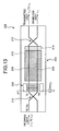
- Fig. 13 is a top view one of an example of the configuration of a conventional acousto-optic tunable filter (AOTF).
- the acousto-optic tunable filter is sometimes referred to simply as optical filter.
- a substrate 204 that composes an acousto-optic tunable filter 202 forms optical waveguide 208 by Ti diffusion with X-cut LiNbO3.
- An acoustic wave is formed by patterning an inter-digital transducer (IDT) 206 that generates acoustic waves.
- IDT inter-digital transducer
- a polarization beam splitter (PBS) 212 is formed by Ti-diffusion etc.
- the incoming light is polarized and separated by the polarization beam splitter (PBS) 212 into two beams, each beam passes through a surface acoustic wave (SAW) guide 210, the two beams are polarized and synthesized by the polarization beam splitter 212, and a transmitted light is output to a transmitting light port.
- SAW surface acoustic wave
- Only the wavelength corresponding to the frequency of SAW generated by the inter-digital transducer (IDT) 206 is polarized and converted when it passes through the SAW guide 210 and output to a branched light port.
- Reference numeral 214 denotes an absorber which absorbs the surface acoustic wave (for example, see patent literature 1).
- the crystal axis is tilted. With the tilting of the crystal axis, the SAW shifts between positive and negative in a cycle.
- This one cycle functions as a just 1/2 wavelength plate for a specific optical wavelength. That is, for an optical signal with a specific wavelength, the microscopic 1/2 wavelength plate looks like alternately tilting at microscopic angles with respect to the crystal axis.
- This is exactly the principle of the FSF (folded Solc filter) (for example, see non-patent literature 3).
- the light signal moves vibrating on a Poincare sphere by FSF and becomes polarized light orthogonal to the incoming polarized light exactly at the SAW guide output point.
- acousto-optic filter comprising a light waveguide for propagating single relative rectilinear polarized light, a surface acoustic wave (SAW) generating means mounted on the optical waveguide for generating an SAW, and an interaction region which distributes a propagation loss of the SAW spatially and converts a specific wavelength component of the single relative rectilinear polarized light propagated in the light waveguide into rectilinear polarized light which crosses this at right angles (for example, see patent literature 2).
- SAW surface acoustic wave
- a wavelength filter with an absorber for absorbing an SAW by each reflective electrode to the outside of the optical waveguide by forming the optical waveguide and excitation electrodes for exciting the SAW on an acousto-optic crystal substrate and disposing reflective electrodes on propagation passage of the SAW.(for example, see patent literature 4).
- a waveguide type optical module for a soaking structure in a module using a waveguide device, a waveguide type optical module is well known, in which a heating/cooling element for controlling the waveguide type optical element temperature via a soaking plate and heat buffer layer is installed on the waveguide type optical element with temperature dependency and at least part of the soaking plate is brought into contact with the waveguide type element (for example, see patent literature 5).
- an arrayed waveguide grating which uses an optical add/drop module comprises, a waveguide chip (including, for example, optical substrate such as silicon, quartz, sapphire, etc.) with an arrayed waveguide (channel waveguide) with optical add/drop functions formed on the surface, a slab waveguide, and a soaking plate which bonds to the rear surface of waveguide chip and soaks waveguide chip, wherein the upper plate for an optical fiber connection is installed to the surface with an arrayed waveguide of a waveguide chip formed (for example, see patent literature 6).
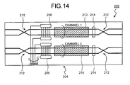
- Fig. 14 is a top view of another example of the configuration of the conventional acousto-optic tunable filter.
- a signal wiring is installed on an inter-digital transducer, when a plurality of optical waveguides are arranged on one substrate, to achieve multichanneling.
- signal wiring installation by fine line patterns is adopted. That is, the acousto-optic tunable optical filter 202 composes a plurality of channels (for example, channels 1, 2) using the configuration same as that shown in Fig. 13 on LiNbO3 substrate 204.
- Fig. 15 is to explain heat resistance of module construction according to a conventional technique.
- the acoust-optic tunable filter 202 of LiNbO3 waveguide type is generally modularized in the following manner. That is, a heater 224, which is a temperature control section, is fixed to a soaking plate 222, for example, copper plate, etc. intervened on the rear surface of the substrate 204 made of X-cut LiNbO3. The entire structure is housed in a package (PKG) 226. Each optical fiber, etc. for optical signals connected to the substrate 204 are pulled out through insertion holes formed in the package 226.
- Reference numeral 230 is a lid which covers an opening at the top surface of package 226.
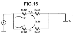
- Fig. 16 is a circuit diagram of a heat equivalent circuit based on Fig. 15.
- the heat conductivity in the module construction of the acousto-optic tunable filter 202 can lead through the heat equivalent circuit shown in Fig. 16 with each element of the package construction taken into account as heat resistance. That is, the heat conductivity is assumed to be obtained by connecting in parallel between current source I and external air Ta serially connected heat resistance RLN0 on the nearly center side of LiNbO3 substrate 204 and upper air resistance RairO on the nearly center side to serially connected heat resistance RLN1 on the edge side of LiNbO3 substrate 204 and upper air resistance Rair1 on the edge side connected in series.
- R1 RLN1+Rair1
- R0 RLN0+Rair0
- ⁇ I (R1+R0) ⁇ T/R1/Rair0
- ⁇ Ts ⁇ T ⁇ (1-(R0-Rair1)/(R1 ⁇ Rair0))
- Th0 is the temperature of the substrate 204 at the center
- Th1 is the temperature of the substrate 204 at the circumference
- ⁇ T is temperature difference from the outside.
- Patent literature 1 Japanese Patent Application Laid-Open Publication No. 2001-330811.
- Patent literature 2 Japanese Patent Application Laid-Open Publication No. H8-146369.
- Patent literature 3 Japanese Patent Application Laid-Open Publication No. H11-326855.
- Patent literature 4 Japanese Patent Application Laid-Open Publication No. H9-49994.
- Patent literature 5 Japanese Patent Application Laid-Open Publication No. 2002-90563.
- Patent literature 6 Japanese Patent Application Laid-Open Publication No. 2000-249853.
- Nonpatent literature 1 Optorics (1999) No. 5, P155.
- Nonpatent literature 2 The Institute of Electronics, Information and Communication Engineers, OPE 96-123, P79.
- Nonpatent literature 3 Optical Waves in Crystal, AMNON YARIV, A Wiley-Interscience Publication, P137.
- patent literature 1 through 4 only to improve the characteristics as a simple AOTF device and they do not consider thermal measures when AOTF is modularized, and they cannot solve problems in multichanneling in which a plurality of AOTFs are positioned on one LiNbO3 substrate.
- the configuration to have a soaking plate to AWG is a generally adopted technique as disclosed in patent literature 5, 6, but because in the AOTF device, the device area is large, there is a problem that a temperature gradient is generated due to the temperature gradient of the heater itself, the difference of heat resistances of air on the device surface, etc., and the desired temperature uniformity cannot be obtained with the soaking plate only.
- the temperature cannot be made uniform by the configuration in which the soaking plate is simply placed on the Peltier element and effects from the outside cannot be eliminated. By the way, when the soaking plate is formed by material with good thermal conductivity, the power consumption of the Peltier element increases.
- An optical device module includes an optical device with a plurality of electrodes disposed at predetermined positions; a substrate disposed oppositely to the optical device and with wiring patterns for connecting to the electrodes; and a wiring which connects the electrodes to the wiring patterns.
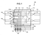
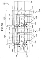
- Fig. 1 is a top view of the essential portions of a module construction of the optical filter related to the first embodiment
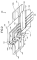
- Fig. 2 is a perspective view of the essential portions of the relevant module construction.
- An optical filter 100 comprises an optical waveguide 108 formed on an X-cut LiNbO3 substrate 101 by Ti diffusion, an inter-digital transducer (IDT) 106 that generates acoustic waves, a polarization beam splitter (PBS) 112, a SAW guide 110, and an absorber 114 that absorbs surface acoustic wave (SAW).
- IDT inter-digital transducer
- PBS polarization beam splitter
- SAW guide 110 polarization beam splitter
- SAW surface acoustic wave
- a soaking structure 102 is disposed on the LiNbO3 substrate 101.
- Bridge substrates (substrates) 103 which compose the soaking structure 102 are disposed oppositely on the surface of the LiNbO3 substrate 101 with specified intervals (spaces).
- Each the bridge substrate 103 is made of ceramics and the specified metals and is formed in a flat plate shape, and covers a wide area (at least, including the inter-digital transducer 106 for each channel, the optical waveguide (optical path) 108 for each channel, the SAW guide 110, and the absorber 114).
- the top surface of the LiNbO3 substrate 101 and the bottom surface of the the bridge substrate 103 have, for example, about 0.5 millimeter (mm) to 2 mm gap, which is the specified interval (space) H.
- the position of an end face 103a on the left side of the illustration of the bridge substrate 103 is set to be a position slightly towards the right from each electrode 107 to expose each electrode (a plurality of electrodes) of the inter-digital transducer 106 for each channel to cover the absorber 114.
- the position of the end face on the right side of the illustration in the bridge substrate 103 is set to become a position rightward from the absorber 114.
- the positions of the end faces at the top and the bottom of the illustration in the bridge substrate 103 are set to be the positions outside from the breadth of the LiNbO3 substrate 101.
- an end face 103b at the lower part of the illustration that is, a plurality of wiring patterns 104 layout-wired from one end face which falls under the input side of high-frequency signals from a signal output means not illustrated, is formed by vacuum deposition technique, etching technique, etc.
- the wiring patterns 104 are made into signal lines of, for example, 50- ⁇ characteristic impedance, by micro strip line, coplanar line, grounded coplanar line, etc.
- the head end of each wiring pattern 104 is directed to the end face 103a on the right side of the illustration and at the same time, establishes a positional one-to-one relation with each electrode 107 of the inter-digital transducer for each channel.
- the wiring pattern 104 By providing the wiring pattern 104 on the bridge substrate 103, installation of wiring on the LiNbO3 substrate 101 is no longer required. In addition, by the use of the region on the bridge substrate 103, the wiring pattern 104 can be freely designed.
- the bridge substrate 103 can be used as the substrate for the wiring pattern 104 from the electrical viewpoint and the strip lines, etc. can be easily formed, and high-density wiring can be carried out, too, with characteristic impedance maintained.
- each wiring pattern 104 to each head end side hanging over the end face 103a of the bridge substrate 103 on the left side of the illustration, one end of connecting energizing cable (wiring) such as wire, etc. is connected, respectively.
- connecting energizing cable such as wire, etc.
- each electrode 107 of the inter-digital transducer 106 for each channel is connected, respectively, in one-to-one relation.
- Connection of each connecting energizing cable 120 is enabled by the use of bonding technique, soldering technique, vacuum deposition technique, etc., but any optional method may be used for the connecting method.
- Each wiring pattern 104 includes signal lines which outputs high-frequency signals to the inter-digital transducer 106 for every channel as well as ground lines.
- the bridge substrate 103 have both top and bottom illustrated end sides of the bottom surface, that is, both end sides which are parallel to the incoming light advancing direction joined to a side wall plate 118 formed into a flat-plate shape with the total length that coincides with the total length of the relevant both ends using ceramics that compose the other part of the soaking structure 102 or a specified metal, etc.
- the bridge substrate 103 and the side wall plate 118 may be of an integral construction. According to the height of the side wall plate 118, there is, for example, about 0.5 mm to 2 mm predetermined interval (space) W between the LiNbO3 substrate 101 and the outer bottom surface (inner surface) of the bridge substrate 103.
- a lead-through block 122 which is slightly lower than the installation height of the bridge substrate 103 and made of ceramics is installed.
- a plurality of wiring patterns 124 are formed, and the head end side of each of them is connected to the head end side of each wiring pattern 104 layout-formed on the bridge substrate 103 via the connection energizing cable (wiring) 126 such as wires, etc. in the one-to-one relation.
- each wiring pattern 124 on the lead-through block 122 a lead wire 128 which communicates with a signal output means not illustrated is connected.
- an insulator 129 comprising ceramics, etc. is disposed for protecting each wiring pattern 124.
- the lead-through block 122 is one example of secondary element for supplying high-frequency signals, etc. to each wiring pattern 104 on the bridge substrate 103, and shall not be limited to the illustrated configuration and a lead-through block which is configured as required from time to time optionally should be used.
- Fig. 3 is a perspective view of the module construction related to the first embodiment and Fig. 4 is an illustration which describes heat resistance of module construction.
- the soaking structure 102 in the first embodiment intends to store the LiNbO3 substrate 101 between both the side wall plates 118 and at the same time fix the side wall plate 118 to a soaking plate 301.
- the bridge substrate 103 and the side wall plate 118 which compose the soaking structure 102 are disposed on the soaking plate 301, for example, about 0.5 mm to 2 mm predetermined interval (space) must be provided between both side surfaces of the LiNbO3 substrate 101, that is, both side surfaces on the side along the incoming light advancing direction and the inner surface of the side wall plate 118 so that the LiNbO3 substrate 101 does not come in direct contact with the side wall plate 118.
- Reference numeral 302 in the drawing denotes a heater, 310 a package, and 310a the inner bottom surface of the package 310.
- heat resistance includes heat resistance RLN0, RLN1 by the LiNbO3 substrate 101, heat resistances Rair1, Rair2, Rair3 of air of each region, heat resistance Rd1 between the soaking plate 301 and the bridge substrate 103, or heat resistance Rd1 between package 310 with high heat conductivity and the bridge substrate 103.
- reference numeral 311 denotes a lid that covers an opening on the top surface of package 310.
- Fig. 5 is a heat equivalent circuit of module construction related to the first embodiment. It is assumed as a heat equivalent circuit in which the heat resistance RLN0 of LiNbO3 substrate and heat resistance Rair2 below the bridge substrate 103 are connected in series, to which Rd1 is connected in parallel, and they are then connected to Rair3 in series, to which heat resistance RLN1 of the LiNbO3 substrate 101 and heat resistance Rair1 of air outside bridge substrate connected in series are connected in parallel between current source I and external air Ta.
- the heat resistances RLN0, RLN1 of the LiNbO3 substrate 101 and the heat resistance Rair2 of the air must be brought to complete agreement.
- the area, etc. in contact with the soaking plate 301 differ, it is, in principle, impossible to bring the heat resistance on the center side of the LiNbO3 substrate 101 in agreement with that on the edge side. This is similar to the phenomenon in the parallel flat plate capacitors in which the capacitance at the edge differs from that at the center due to the edge effect.
- the bridge substrate 103 is used, and by fixing the bridge substrate 103 to the soaking plate 301, the temperature Th0 can be raised when temperature on the center side of the LiNbO3 substrate 101 is low, and a temperature gradient on LiNbO3 substrate 103 is eliminated, and the surface temperature can be kept uniformly throughout the whole surface.
- line design laminate design
- the wiring pattern 104 is formed on the bridge substrate 103, line design (layout design) to bring the characteristic impedance of the wiring pattern 104 to 50 ⁇ can be easily carried out, and it becomes possible to prevent signal degradation and generation of cross-talks, and multichanneling can be promoted.
- FIG. 6 is a perspective view of a module construction related to the second embodiment. Elements similar to those of the first embodiment are given like reference numerals. For convenience, the description of the lead-through block 122 is omitted.
- the LiNbO3 substrate 101 is housed between the side wall plates 118 and disposed and fixed to the inner bottom surface 310a of the package 310.
- the heater 302, the soaking plate 301, and the LiNbO3 substrate 101 are laminated in that order from the bottom.
- the bridge substrate 103 is fixed to the package 310 in this way, it must be arranged in such a manner that, for example, about 0.5 mm to 2 mm predetermined intervals (spaces) must be provided between both side surfaces (and the heater 302 and soaking 301) on the side along the incoming light advancing direction and between each side wall plate 118 and the inner surface.
- Fig. 7 is a heat equivalent circuit diagram of the module construction related to the second embodiment.
- Rd1 is a heat resistance between the package 310 and the bridge substrate 103.
- the heat resistance Rd1 is small and it is possible to indicate the heat resistance Rair0 (Rair2, Rair3 in Fig. 7) from the LiNbO3 substrate 101 to the lid 311 (not shown), which serves as the top surface of the package 310 seemingly small, and to lower the temperature ThO at the center side of the LiNbO3 substrate 101.
- Th0 Th1
- the temperature Th0 can be lowered when the temperature on the center side of the LiNbO3 substrate 103 is high, and a temperature gradient on the LiNbO3 substrate 101 can be eliminated, and the surface temperature can be maintained uniformly.
- the wiring pattern 104 is formed on the bridge substrate 103, it is possible to easily design the line (design the layout) with 50 ⁇ characteristic impedance of the wiring pattern 104, and at the same time, it is possible to prevent signal degradation as well as to prevent generation of cross-talks, and thereby to promote multichanneling.
- the third embodiment intends to cancel the temperature gradient of the LiNbO3 substrate in the configuration in which optical waveguides that compose the AOTF filter on LiNbO3 substrate are connected in series in a plurality of stages in order to improve the filter characteristics. Configurations similar to the first embodiment are given like reference numerals.
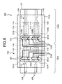
- Fig. 8 is a top view of the essential portions of the module construction of optical filter related to the third embodiment.
- the optical filter 100 includes an optical filter 100A on the preceding step connected in series to an optical filter 100B on the latter stage of the similar configuration.
- Optical output of the optical filter 100A is input into the optical filter 100B.
- the optical filter 100A comprises an inter-digital transducer 106A, the optical waveguide (optical path) 108, the SAW guide 110, the absorber 114, the polarization beam splitter 112, etc.
- the optical filter 100B comprises an inter-digital transducer 106B, the optical waveguide (optical path) 108, the SAW guide 110, the absorber 114, the polarization beam splitter 112, etc.
- optical filters of other channels arranged in parallel at the upper and lower positions in the drawing are connected in series in the same manner (2 channels in total).
- the bridge substrate 103 which composes part of the soaking structure 102 is arranged oppositely with a predetermined interval (space) provided.
- This bridge substrate 103 covers a wide range including the optical waveguide (optical path) 108, the inter-digital transducer 106, the SAW guide 110, and the absorber 114 for each channel formed on the LiNbO3 substrate 101.
- the interval same as that of the first embodiment is provided (for example, about 0.5 mm to 2 mm).
- elongated openings 801 A, 801 B which enable the electrodes 107A, 107B of each channel to be seen en bloc are formed near right and left edges, that is, near the edges corresponding to the direction before and after the incoming light advancing direction and at the position right above each electrode (a plurality of electrodes) 107A, 107B of the inter-digital transducer for every channel.
- wiring patterns 104A, 104B are formed by vacuum deposition techniques, etching techniques, etc. with the end face 103b used as one end same as in the first embodiment.
- the other end of the wiring pattern 104A is bent and led through in the left direction in the figure in the midway towards the opening 801A for the optical filter 100A of the preceding step, while the other end of the wiring pattern 104B is bent and led through in the right direction in the drawing in the midway towards the opening 801B for the optical filter 100B of the latter step.
- Each electrode 107A, 107B of the inter-digital transducers 106A, 106B for each channel and other end of each wiring pattern 104A, 104B are connected by connection energizing cable 120 such as wire, etc. via the openings 801A, 801 B.
- the soaking structure 102 can be disposed in two ways: fixed on the soaking plate 301 (see Fig. 3) as described in the first embodiment or the second embodiment and fixed on the inner bottom surface 310a of the package 310 (see Fig. 6). How to dispose the soaking structure 102 can be chosen based on the relation between the temperature Th0 on the center side of the LiNbO3 substrate 101 and the temperature Th1 on the end side (that is, end face side).
- the third embodiment when optical filters are multi-channeled by serial connection or parallel arrangement of a plurality of channels, electrical connection can be easily carried out by providing the openings 801A, 801B for the signal connection sections only, in addition to the effects described in the first and the second embodiments that the temperature of the LiNbO3 substrate 101 can be homogenized and signal loss can be reduced, and others.
- the wiring patterns 104A, 104B on single the bridge substrate 103 for each of the electrodes 107A, 107B of the inter-digital transducers 106A, 106B disposed in the optical filters 100A, 100B arranged in series or in parallel, and improve the packaging capability, and requirements for multichanneling can be easily responded.
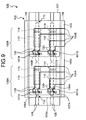
- FIG. 9 is a top view of the configuration of the essential portions of the module construction of an optical filter related to the fourth embodiment.
- the fourth embodiment differs from the third embodiment in the shape of the bridge substrate 103 which composes the soaking structure 102, and the configuration of optical filter 100 is the same as that of the third embodiment and the detailed description will be omitted.
- the optical filter 100 has the optical filter 100A on the preceding step connected in series to the optical filter 100B on the latter stage of the similar configuration, and optical output of the optical filter 100A is input into the optical filter 100B.
- the bridge substrate 103 which composes part of the soaking structure 102 is arranged oppositely with a predetermined interval (space) provided.
- This bridge substrate 103 covers a wide range including the optical waveguide (optical path) 108, the inter-digital transducer 106, the SAW guide 110, and the absorber 114 for each channel formed on the LiNbO3 substrate 101.
- openings 901 A, 901 B which enable the electrode 107A, 107B of each channel to be seen en bloc are formed near left edge and at the center position, that is, at the position right above each electrode 107A, 107B of the inter-digital transducer for every channel.
- the wiring patterns 104A, 104B are formed by vacuum deposition techniques, etching techniques, etc. with the end face 103b used as one end same as in the first embodiment.
- the other end of the wiring pattern 104A, 1048 are bent and led through in the left direction in the figure in the midway towards the openings 901A, 901B for the optical filters 100A, 100B, respectively.
- Each electrode 107A, 107B of the inter-digital transducers 106A, 106B for each channel and other end of each wiring pattern 104A, 104B are connected by connection the energizing cable 120 such as wire, etc. via openings 901A, 901B.
- the soaking structure 102 has a mode in which it is disposed and fixed to the soaking plate 301 (see Fig. 3) as described in the first embodiment or the second embodiment and a mode in which it is disposed and fixed to the inner bottom surface 310a of the package 310 (see Fig. 6).
- Which mode to be employed is chosen by the relation between the temperature Th0 on the center side of the LiNbO3 substrate 101 and the temperature Th1 on the end side (that is, end face side).
- the wiring patterns 104A, 104B on single the bridge substrate 103 for each of the electrodes 107A, 107B of the inter-digital transducers 106A, 106B disposed in the optical filters 100A, 100B arranged in series or in parallel, and improve the packaging capability, and requirements for multichanneling can be easily responded.
- wiring patterns are compared between the third embodiment and the fourth embodiment, in the end face 103b section of the bridge substrate 103, in the third embodiment, all the wiring patterns 104A, 104B can be brought together, while in the fourth embodiment, the wiring pattern 104A for the optical filter 100A of the preceding step and the wiring pattern 104B for the optical filter 100B of the latter step connected in series can be separated and arranged.
- the configuration of the fifth embodiment is to separate the bridge substrate 103 which composes the soaking structure 102 when multi-channeling is carried out.
- Fig. 10 is a top view of the configuration of the essential portions of the module structure of an optical filter (ADTF) related to the fifth embodiment.
- the soaking structure is divided (in other words, two soaking structures are provided) nearly at the center position as compared to the configuration of the fourth embodiment (see Fig. 9).
- a soaking structure 102A is provided for the optical filter 100A, while a soaking structure 102B is provided for the optical filter 100B.
- bridge substrates 103A, 103B which comprise part of soaking structures 102A, 102B of the preceding step and the latter step may have illustrated the end face 103a on the left side, respectively, located at the position slightly rightward from relevant electrodes 107A, 107B so that the electrodes 107A, 107B of the inter-digital transducer 106A, 106B for each channel are exposed.
- Other reference numerals in the drawing are same as those of each embodiment described above and the explanation will be omitted.
- temperature can be homogenized at least within the function section of the optical filter and if characteristics degradation caused by the temperature gradient can be avoided, the soaking structure 102 can be divided and installed in units of function sections of this optical filter.
- the configuration of the soaking structure can be made simple and the manufacturing cost can be suppressed.
- FIG. 11 is a top view of the configuration of the essential portions of the module construction of the optical filter related to the sixth embodiment.
- the position of the end face of illustrated the end face 103a on the left side of the bridge substrate 103A which composes part of the soaking structure 102A is set to be the position slightly rightward from each electrode 107A of the inter-digital transducer 106A of the optical filter 100A.
- the position of illustrated end face 103c on the right side of the bridge substrate 103A covers the absorber 114 of the optical filter 100A and the polarization beam splitter 112, and others, and is set to the illustrated position leftward from each electrode 107B of the inter-digital transducer 106B of the optical filter 100B.
- the wiring pattern 104A for the optical filter 100A and the wiring pattern 104B for the optical filter 100B are formed.
- the head end of the wiring pattern 104A is directed to the end face 103a on the left side in the illustration and is patterned to achieve the one-to-one relation with respect to each electrode 107A of the inter-digital transducer 106A for each channel of the optical filter 100A.
- the head end of the wiring pattern 104B is directed to end face 103c on the right side in the illustration and is patterned to achieve the one-to-one relation with respect to each electrode 107B of the optical filter 100B.
- the sixth embodiment when multichanneling is carried out, it is possible to supply signals to the inter-digital transducer 106A, 106B of optical filters 100A, 100B using one one soaking structure 102A.
- the soaking structure 102B which has no wiring patterns and connection energizing cables but other configurations same as those of the soaking structure 102A should be disposed.
- the seventh embodiment is a configuration example when still more multi-channeling is carried out.
- Fig. 12 is a top view of the configuration of the essential portions of the module construction of the optical filter related to the seventh embodiment.
- One-channel waveguide 108 is composed by serial connection of optical filters 100A, 100B and waveguides for four channels are arranged.
- the number of parallel arrangements is increased in the longitudinal direction of the figure.
- the soaking structure 102 is formed in the width that corresponds to the width (length in the longitudinal direction in the figure) of the LiNbO3 substrate 101 formed by the number of channels arranged in parallel.
- the wiring patterns 104A, 104B should be formed in the number that correspond to the number of channels (strictly speaking, number of terminals of electrode 107A, 107B of the inter-digital transducer 106A, 106B on the LiNbO3 substrate 101).
- the soaking structure 102 should be formed in the length (length in the lateral direction in the figure) that corresponds to the number of serial connections of optical filters.
- space H between the surface of the LiNbO3 substrate 101 and the bottom surface of the bridge substrate 103 and space W between the LiNbO3 substrate 101 and the side wall plate 118 (for both, see Fig. 2) must be provided as described above so that the soaking structure 102 does not come in direct contact with the LiNbO3 substrate 101.
- the construction of the bridge substrate 103 shown in Fig. 12 corresponds to the configuration in which the openings 801A, 801B which enable the electrode 107A, 107B of each channel to be seen en bloc are formed at the position right above each electrode 107A, 107B of the inter-digital transducer described in the third embodiment and the number of channels is further increased.
- the configuration of the bridge substrate 103 may have the layout of wiring patterns changed as shown in the fourth embodiment even when multi-channeling is carried out or as explained in the fifth and the sixth embodiments, bridge substrates may be provided in the number that is same as the number of the optical filters. By the way, filters of different channels arranged up and bottom in the figure may be connected in series via bent waveguide (not illustrated).
- the case when the number of channels is increased to achieve multi-channeling, the case can be met only by changing the size of the soaking structure in accordance with the change of the size of LiNbO3 substrate.
- connection energizing cables are used for wiring patterns on the bridge substrate which compose part of the soaking structure, specific examples to have openings in the bridge substrate or to enable wiring connection of connection energizing cables by forming wiring patterns on the end face of the bridge substrate and using the relevant end face were shown.
- a through hole that penetrates the bridge substrate itself from the head end side of wiring pattern of the top surface of the bridge substrate is formed to insert the through electrode, and the through electrode is connected to each electrode of inter-digital transducer.
- a flange or latching piece, etc. may be provided on one end for positioning as well as for easy connection work.
- the temperature of the device (for example, waveguide type optical device) is intended to achieve uniformity by the use of a bridge substrate, and satisfactory performance of the device can be maintained.
- wring patterns for supplying high-frequency signals, etc. to a waveguide type device are layout-designed and formed on the bridge substrate (soaking structure)
- line design of 50 ⁇ characteristic impedance of wiring patterns can be carried out, signal degradation can be prevented, and generation of cross-talks can be prevented.
- multi-channeling it is not necessary to secure a region for wiring patterns on the waveguide type optical device, it is not necessary to secure a region for installing wiring on the LiNbO3 substrate, either, an increase in the size of the LiNbO3 substrate can be avoided, and multi-channeling can be still more promoted.
- degradation of signals supplied to optical devices can be prevented, exhibiting an effect that the temperature of optical devices can be homogenized.
- effects of homogenizing the temperature of optical device and preventing cross-talks from occurring between adjacent wiring patterns while avoiding an increase of wiring line regions can be achieved.
Landscapes
- Physics & Mathematics (AREA)
- Nonlinear Science (AREA)
- General Physics & Mathematics (AREA)
- Optics & Photonics (AREA)
- Optical Modulation, Optical Deflection, Nonlinear Optics, Optical Demodulation, Optical Logic Elements (AREA)
- Optical Integrated Circuits (AREA)
- Semiconductor Lasers (AREA)
- Light Receiving Elements (AREA)
Applications Claiming Priority (2)
| Application Number | Priority Date | Filing Date | Title |
|---|---|---|---|
| JP2003362531A JP4727916B2 (ja) | 2003-10-22 | 2003-10-22 | 光デバイスモジュール |
| JP2003362531 | 2003-10-22 |
Publications (3)
| Publication Number | Publication Date |
|---|---|
| EP1526402A2 true EP1526402A2 (fr) | 2005-04-27 |
| EP1526402A8 EP1526402A8 (fr) | 2005-07-27 |
| EP1526402A3 EP1526402A3 (fr) | 2006-08-02 |
Family
ID=34386513
Family Applications (1)
| Application Number | Title | Priority Date | Filing Date |
|---|---|---|---|
| EP04007642A Withdrawn EP1526402A3 (fr) | 2003-10-22 | 2004-03-30 | Module à dispositif optique |
Country Status (3)
| Country | Link |
|---|---|
| US (1) | US7151866B2 (fr) |
| EP (1) | EP1526402A3 (fr) |
| JP (1) | JP4727916B2 (fr) |
Families Citing this family (6)
| Publication number | Priority date | Publication date | Assignee | Title |
|---|---|---|---|---|
| JP6318715B2 (ja) * | 2014-03-07 | 2018-05-09 | 富士通オプティカルコンポーネンツ株式会社 | 光モジュール |
| JP2015172683A (ja) * | 2014-03-12 | 2015-10-01 | 富士通オプティカルコンポーネンツ株式会社 | 光モジュール |
| JP6288144B2 (ja) * | 2016-04-01 | 2018-03-07 | 住友大阪セメント株式会社 | 光変調器 |
| CN109638638B (zh) * | 2017-10-05 | 2023-06-13 | 住友电工光电子器件创新株式会社 | 光学模块 |
| US11209673B2 (en) * | 2019-10-30 | 2021-12-28 | Taiwan Semiconductor Manufacturing Company, Ltd. | Heater structure configured to improve thermal efficiency in a modulator device |
| WO2021250760A1 (fr) * | 2020-06-08 | 2021-12-16 | 日本電信電話株式会社 | Module optique |
Citations (3)
| Publication number | Priority date | Publication date | Assignee | Title |
|---|---|---|---|---|
| EP1094355A1 (fr) | 1999-10-19 | 2001-04-25 | Corning Incorporated | Interconnexion electrique de circuits planaires à ondes lumineuses |
| EP1191361A1 (fr) | 2000-09-25 | 2002-03-27 | Sumitomo Electric Industries, Ltd. | Module de chauffage pour un dispositif de guide d'ondes |
| US6522793B1 (en) | 2001-11-21 | 2003-02-18 | Andrei Szilagyi | Low voltage electro-optic modulator with integrated driver |
Family Cites Families (21)
| Publication number | Priority date | Publication date | Assignee | Title |
|---|---|---|---|---|
| JPS61190322A (ja) | 1985-02-20 | 1986-08-25 | Matsushita Electric Ind Co Ltd | 光スイッチ |
| US5032897A (en) * | 1990-02-28 | 1991-07-16 | International Business Machines Corp. | Integrated thermoelectric cooling |
| JPH04212442A (ja) * | 1990-09-07 | 1992-08-04 | Japan Computer Aid:Kk | 性能増強icパッケージング構造体 |
| JPH08143369A (ja) | 1994-11-18 | 1996-06-04 | Takasago Ind Co Ltd | 陶磁器焼成用支承具 |
| IT1277412B1 (it) | 1995-08-02 | 1997-11-10 | Pirelli Cavi S P A Ora Pirelli | Dispositivo acusto-ottico in guida d'onda sintonizzabile a risposta indipendente dalla polarizzazione e metodo di trattamento acusto- |
| JP3633045B2 (ja) | 1995-08-07 | 2005-03-30 | 富士通株式会社 | 波長フィルタ |
| JPH09138325A (ja) * | 1995-11-13 | 1997-05-27 | Nec Corp | 光ファイバ実装構造とその製造方法 |
| JP3047352B2 (ja) * | 1996-06-28 | 2000-05-29 | 日本電気株式会社 | 温度制御型光結合構造 |
| JP3836950B2 (ja) | 1997-07-02 | 2006-10-25 | 富士通株式会社 | 音響光学デバイス |
| JP3165106B2 (ja) | 1998-05-19 | 2001-05-14 | 日本電気株式会社 | 光可変波長フィルタ |
| JP2000075152A (ja) | 1998-08-31 | 2000-03-14 | Furukawa Electric Co Ltd:The | 光モジュール |
| JP2000249853A (ja) | 1999-02-26 | 2000-09-14 | Furukawa Electric Co Ltd:The | 光モジュール |
| US6477284B1 (en) * | 1999-06-14 | 2002-11-05 | Nec Corporation | Photo-electric combined substrate, optical waveguide and manufacturing process therefor |
| JP4435378B2 (ja) | 2000-05-22 | 2010-03-17 | 富士通株式会社 | 音響光学チューナブルフィルタ |
| JP4454817B2 (ja) | 2000-09-18 | 2010-04-21 | 株式会社フジクラ | 導波路型光モジュール |
| JP2002131712A (ja) * | 2000-10-19 | 2002-05-09 | Mitsubishi Electric Corp | 光デバイスおよびその製造方法 |
| CA2365804A1 (fr) * | 2000-12-22 | 2002-06-22 | Mitsuru Yamamoto | Dispositif de commande de trajet optique a section reflechissante, et methode de fabrication |
| JP2003005138A (ja) * | 2001-06-18 | 2003-01-08 | Hitachi Cable Ltd | 導波路型光合分波器 |
| JP3931703B2 (ja) * | 2001-12-27 | 2007-06-20 | 株式会社日立製作所 | 光学素子搭載基板及びその製造方法 |
| JP2003227946A (ja) * | 2002-02-01 | 2003-08-15 | Sumitomo Electric Ind Ltd | 光モジュール |
| JP4467280B2 (ja) * | 2003-10-22 | 2010-05-26 | 富士通株式会社 | 光デバイスモジュール |
-
2003
- 2003-10-22 JP JP2003362531A patent/JP4727916B2/ja not_active Expired - Lifetime
-
2004
- 2004-03-24 US US10/807,520 patent/US7151866B2/en not_active Expired - Lifetime
- 2004-03-30 EP EP04007642A patent/EP1526402A3/fr not_active Withdrawn
Patent Citations (3)
| Publication number | Priority date | Publication date | Assignee | Title |
|---|---|---|---|---|
| EP1094355A1 (fr) | 1999-10-19 | 2001-04-25 | Corning Incorporated | Interconnexion electrique de circuits planaires à ondes lumineuses |
| EP1191361A1 (fr) | 2000-09-25 | 2002-03-27 | Sumitomo Electric Industries, Ltd. | Module de chauffage pour un dispositif de guide d'ondes |
| US6522793B1 (en) | 2001-11-21 | 2003-02-18 | Andrei Szilagyi | Low voltage electro-optic modulator with integrated driver |
Also Published As
| Publication number | Publication date |
|---|---|
| EP1526402A8 (fr) | 2005-07-27 |
| EP1526402A3 (fr) | 2006-08-02 |
| US7151866B2 (en) | 2006-12-19 |
| US20050089275A1 (en) | 2005-04-28 |
| JP4727916B2 (ja) | 2011-07-20 |
| JP2005128185A (ja) | 2005-05-19 |
Similar Documents
| Publication | Publication Date | Title |
|---|---|---|
| US8285149B2 (en) | Method and system for integrated DWDM transmitters | |
| US9229292B2 (en) | Optical module and optical transmitter | |
| US6895135B2 (en) | Optical waveguide device and method of manufacture thereof | |
| US6922508B2 (en) | Optical switching apparatus with adiabatic coupling to optical fiber | |
| SK47496A3 (en) | Acoustic-optical waveguide for division acording to the wave lenght | |
| JP3896905B2 (ja) | 光通信装置 | |
| US6816296B2 (en) | Optical switching network and network node and method of optical switching | |
| US7151866B2 (en) | Optical device module | |
| JP2000019345A (ja) | 光集積モジュール | |
| JP6228064B2 (ja) | 光モジュール | |
| JP2005128184A (ja) | 光デバイスモジュール | |
| CN115621839B (zh) | 一种激光装置及其制作方法 | |
| US11489611B2 (en) | Reconfigurable optical add-drop multiplexer with low power consumption | |
| US7430344B2 (en) | Acousto-optic device and fabrication method of acousto-optic device | |
| JPH11119177A (ja) | 光時間多重変調送信器モジュール | |
| JP3116900B2 (ja) | 電子冷却器およびこれを用いた光部品モジュール | |
| US6813433B2 (en) | Method for manufacturing optical waveguide and optical waveguide device, optical waveguide device and optical waveguide, and optical communication apparatus using optical waveguide device | |
| JP4090295B2 (ja) | 光スイッチモジュールおよびその製造方法 | |
| JPH02214828A (ja) | 集積化光導波路デバイス | |
| JP2000075152A (ja) | 光モジュール | |
| US8098999B2 (en) | Multiple channel power monitor | |
| JP2000329954A (ja) | アレイ導波路格子 | |
| JP2000019344A (ja) | 光モジュール | |
| CN121399531A (zh) | 光波导元件及使用其的光调制器以及光发送装置 | |
| JP2003185858A (ja) | 波長分波器およびそれを用いた波長分波スイッチ |
Legal Events
| Date | Code | Title | Description |
|---|---|---|---|
| PUAI | Public reference made under article 153(3) epc to a published international application that has entered the european phase |
Free format text: ORIGINAL CODE: 0009012 |
|
| AK | Designated contracting states |
Kind code of ref document: A2 Designated state(s): AT BE BG CH CY CZ DE DK EE ES FI FR GB GR HU IE IT LI LU MC NL PL PT RO SE SI SK TR |
|
| AX | Request for extension of the european patent |
Extension state: AL LT LV MK |
|
| RIN1 | Information on inventor provided before grant (corrected) |
Inventor name: NAKAZAWA, TADAO Inventor name: MIYATA, HIDEYUKIC/O FUJITSU LIMITED Inventor name: AKIMOTO, KAZUAKIFUJITSU NETWORK TECHNOLOGIES LTD. Inventor name: AOTA, HIROFUMIFUJITSU NETWORK TECHNOLOGIES LTD. Inventor name: OIKAWA, YOICHIFUJITSU NETWORK TECHNOLOGIES LTD. |
|
| PUAL | Search report despatched |
Free format text: ORIGINAL CODE: 0009013 |
|
| AK | Designated contracting states |
Kind code of ref document: A3 Designated state(s): AT BE BG CH CY CZ DE DK EE ES FI FR GB GR HU IE IT LI LU MC NL PL PT RO SE SI SK TR |
|
| AX | Request for extension of the european patent |
Extension state: AL LT LV MK |
|
| 17P | Request for examination filed |
Effective date: 20061116 |
|
| AKX | Designation fees paid |
Designated state(s): DE FR GB |
|
| 17Q | First examination report despatched |
Effective date: 20071106 |
|
| STAA | Information on the status of an ep patent application or granted ep patent |
Free format text: STATUS: THE APPLICATION IS DEEMED TO BE WITHDRAWN |
|
| 18D | Application deemed to be withdrawn |
Effective date: 20110818 |