EP1522211B1 - Steuerschaltung zum steuern einer elektronenemissionsvorrichtung - Google Patents
Steuerschaltung zum steuern einer elektronenemissionsvorrichtung Download PDFInfo
- Publication number
- EP1522211B1 EP1522211B1 EP03798135A EP03798135A EP1522211B1 EP 1522211 B1 EP1522211 B1 EP 1522211B1 EP 03798135 A EP03798135 A EP 03798135A EP 03798135 A EP03798135 A EP 03798135A EP 1522211 B1 EP1522211 B1 EP 1522211B1
- Authority
- EP
- European Patent Office
- Prior art keywords
- current
- input
- control circuit
- excitation current
- threshold value
- Prior art date
- Legal status (The legal status is an assumption and is not a legal conclusion. Google has not performed a legal analysis and makes no representation as to the accuracy of the status listed.)
- Expired - Lifetime
Links
Images

Classifications
-
- B—PERFORMING OPERATIONS; TRANSPORTING
- B82—NANOTECHNOLOGY
- B82Y—SPECIFIC USES OR APPLICATIONS OF NANOSTRUCTURES; MEASUREMENT OR ANALYSIS OF NANOSTRUCTURES; MANUFACTURE OR TREATMENT OF NANOSTRUCTURES
- B82Y10/00—Nanotechnology for information processing, storage or transmission, e.g. quantum computing or single electron logic
-
- H—ELECTRICITY
- H05—ELECTRIC TECHNIQUES NOT OTHERWISE PROVIDED FOR
- H05G—X-RAY TECHNIQUE
- H05G1/00—X-ray apparatus involving X-ray tubes; Circuits therefor
- H05G1/08—Electrical details
- H05G1/26—Measuring, controlling or protecting
- H05G1/30—Controlling
-
- G—PHYSICS
- G09—EDUCATION; CRYPTOGRAPHY; DISPLAY; ADVERTISING; SEALS
- G09G—ARRANGEMENTS OR CIRCUITS FOR CONTROL OF INDICATING DEVICES USING STATIC MEANS TO PRESENT VARIABLE INFORMATION
- G09G3/00—Control arrangements or circuits, of interest only in connection with visual indicators other than cathode-ray tubes
- G09G3/20—Control arrangements or circuits, of interest only in connection with visual indicators other than cathode-ray tubes for presentation of an assembly of a number of characters, e.g. a page, by composing the assembly by combination of individual elements arranged in a matrix no fixed position being assigned to or needed to be assigned to the individual characters or partial characters
- G09G3/22—Control arrangements or circuits, of interest only in connection with visual indicators other than cathode-ray tubes for presentation of an assembly of a number of characters, e.g. a page, by composing the assembly by combination of individual elements arranged in a matrix no fixed position being assigned to or needed to be assigned to the individual characters or partial characters using controlled light sources
-
- H—ELECTRICITY
- H01—ELECTRIC ELEMENTS
- H01J—ELECTRIC DISCHARGE TUBES OR DISCHARGE LAMPS
- H01J2201/00—Electrodes common to discharge tubes
- H01J2201/30—Cold cathodes
- H01J2201/304—Field emission cathodes
- H01J2201/30446—Field emission cathodes characterised by the emitter material
- H01J2201/30453—Carbon types
- H01J2201/30469—Carbon nanotubes (CNTs)
-
- H—ELECTRICITY
- H01—ELECTRIC ELEMENTS
- H01J—ELECTRIC DISCHARGE TUBES OR DISCHARGE LAMPS
- H01J2237/00—Discharge tubes exposing object to beam, e.g. for analysis treatment, etching, imaging
- H01J2237/06—Sources
- H01J2237/063—Electron sources
- H01J2237/06325—Cold-cathode sources
- H01J2237/06341—Field emission
- H01J2237/0635—Multiple source, e.g. comb or array
-
- H—ELECTRICITY
- H01—ELECTRIC ELEMENTS
- H01J—ELECTRIC DISCHARGE TUBES OR DISCHARGE LAMPS
- H01J2237/00—Discharge tubes exposing object to beam, e.g. for analysis treatment, etching, imaging
- H01J2237/06—Sources
- H01J2237/065—Source emittance characteristics
Definitions
- the present invention relates to a control circuit for controlling an electron emission device.
- the present invention relates to a control circuit used to control so-called carbon Nano Tubes arranged in an array are suitable is.
- IC Integrated Circuit
- lithography in a wholly applied to a wafer Lacquer with the help of a mask, which in certain places either is opaque or transparent.
- a light beam of a predetermined wavelength generated, with the help of optical lenses under utilization the phenomenon of refraction with a special arrangement focused and then aimed at the wafer to the to expose there applied paint.
- the with the help of this Technology achievable resolution depends on the wavelength of light from. The smaller the wavelength of light, the better smaller feature sizes can be achieved.
- the wavelength of light can because of optical transmission characteristics
- the lenses used for light focusing are not be mitverkleinert at will.
- electrons be used instead of light for irradiation of the paint.
- the electrons from a suitable electron emission device emitted, suitably focused and directed to the wafer.
- a very small Paint area pixels
- multiple electron emission devices to one Array to summarize even larger paint areas to be able to irradiate simultaneously and specifically, so that the desired small structures faster than when using produced by only one electron emission device can be.
- a Braunsche Use tube for electron emission that's how it is for a person skilled in the obvious that already due to the necessarily large physical dimension of a Such arrays are produced only very coarse structures could. For this reason, one is on electron emission devices instructed to have small dimensions, such as the aforementioned Carbon Nano Tubes.
- the Carbon Nano Tubes are essentially around several mostly cylindrical carbon structures with a diameter of a few nanometers on one Substrate are arranged and have a control electrode. Is now this control electrode an electrical Control voltage of, for example, some 10V applied, so the CNT pick up an excitation current. The at the The tip of this carbon fiber formation created field a field emission of the electrons.
- the CNTs are advantageous, because now an array of electron beams are generated can, compared with the desired small structures generated faster to a single electron beam because one CNT array is multiple at a time Can irradiate pixels on the wafer.
- the object of the present invention is to provide a Control circuit and a method for controlling an electron emission device and also an array for controlling a multi-electron emission device to provide which allow high-resolution irradiation.
- control circuit according to claim 1, a method of controlling an electron emission device according to claim 15 or an array for controlling a multi-electron emission device according to claim 16 solved.
- the present invention is based on the recognition that a high resolution with a example of CNT existing Array is achievable by the CNT individually or even in smaller groups comprising some CNT, be provided with a control circuit, wherein the control circuit clearly the emitted electron dose based an excitation current picked up by the CNT, to reach the desired dose when the desired dose is reached Disable CNT.
- the magnitude of the excitation current to determine whether the corresponding CNTs are even capable of within a predetermined period of time a sufficient To deliver a dose. If the amount of the excitation current is too high small, the control circuit according to the invention becomes the disable corresponding CNT, so no unfinished Points etc. are generated on the wafer.
- the amount of charge emitted by the CNT depends on the amount of an excitation current picked up by these CNTs becomes. To determine the amount of charge emitted by the CNT Therefore, this excitation current can be used become. This is exploited that of a current transported cargo within a time interval an integral over the current curve within this time interval can be determined. To determine if one certain amount of charge has been emitted by the CNT, However, it is sufficient to monitor whether this amount of charge has reached a predetermined charge threshold. is reaches this charge threshold, the CNT can be switched off be switched off by the excitation current becomes. Proper functioning of the CNT will also work determined on the basis of the excitation current by being monitored whether the amount of the excitation current is a predetermined Current threshold reached. Will this current threshold not achieved, it is synonymous with that is necessary for paint irradiation charge amount within a predetermined time interval from the CNT can not be emitted. The CNT can in this case be deactivated by turning off the excitation current becomes.
- An advantage of the present invention is that the control circuit for controlling the CNT on the basis of two measurable quantities is executed, namely the amount of the excitation current and that of the excitation current transported Charge amount.
- comparators are used to monitor whether the amount of the excitation current is a predetermined one Current threshold reached as well as whether by the excitation current transported amount of charge a predetermined charge threshold reached. As it is the comparators is standard components, the inventive Control circuit therefore be realized inexpensively.
- Another advantage of the present invention is in that both the magnitude of the excitation current and the amount of charge transported by the excitation current can be monitored very closely, because this is not necessarily the excitation current itself used must become. According to one embodiment are with Help a current mirror generates several auxiliary currents, the in a predetermined relationship to the excitation current are. On the basis of these auxiliary currents are without a Influencing the excitation current both the amount of Excitation current and the amount of charge monitored.
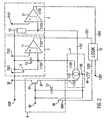
- Fig. 1 shows an arrangement consisting of an electron emission device 1, which is to be controlled by a control circuit 3 according to the invention.
- the latter comprises means 5 which monitors whether the amount of excitation current 4 received by the electron emission device 1 exceeds a predetermined current threshold.
- the control circuit 3 further includes means 7 for monitoring whether the amount of charge emitted by the electron emission device exceeds a predetermined charge threshold.
- the control circuit for controlling an electron emission device according to the present invention further includes means 9 for turning off the exciting current, by means of which the electron emission device 1 is turned off by turning off the exciting current 4 in case of exceeding the charging threshold or undercutting the current threshold.
- the device 9 for switching off the excitation current can be switched on again by means of a not shown in Fig.
- FIG. 1 shows a preferred embodiment of the invention, wherein the device 9, the device 5 and the means 7 for determining the charge threshold are marked in dashed lines.
- the means 9 for switching off the excitation current consists essentially of a transistor 91, as High-voltage transistor can be executed, with a control input 93, an input 95 and an output 97.
- the Input 95 of transistor 91 is not one with in Fig. 2 drawn control electrode of an electron emission device connected, in such a way that the excitation current regarding its technical current direction in these Inlet can flow - the electron emission device takes this excitation current with respect to its physical Current direction.
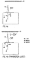
- Fig. 4a shows a schematic representation of the transistor 91 with a CNT 40, which is near a to be exposed Substrate 42 is arranged.
- the "rest" of the control circuit is not shown in detail in Figure 4a. Only By way of example, it is assumed below that the transistor 91 is a self-blocking N-MOSFET.
- the substrate to be exposed is related to a potential Mass of z. B. brought some 10 V to +50 V, which corresponds to a typical operating voltage for CNTs.
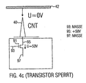
- Fig. 4c shows the situation in which the control input 93 of the transistor 91 is at ground (0 V), the transistor so locks. In this case, fall between the substrate 42 and the CNT no voltage, so no electrons emitted by the CNT.
- the voltage on the substrate 42 has an amount of typically a few 10 volts to 50V sufficient to due to the field emission the electrons from the tip a source including the electron emission device, to let escape. This is the case with the CNT 40 Source of some mostly cylindrical carbon formations with a diameter of a few nanometers, which is up a substrate.
- a voltage for controlling the conductivity of the transistor 91 can be applied. Is this voltage applied so the e.g. self-locking transistor 91 "on”, and the excitation current flowing into the input 95 forwarded to the output 97. Is the transistor 91 self-guiding, so it is by the applied voltage "off", causing the excitation current is no more flows.
- control input 93 If the control input 93 is connected to a mass M, then transistor 91 goes into a blocking state and thus shuts off the excitation current. Only optional between the control input 93 and the mass M a capacitor C1, which is used to "store" the voltage at the Node 93 of the transistor 91 is used.
- the means 9 for switching off the excitation current includes Further, an optional switch 99, the between the control input 93 and the mass M is connected, and further comprising a control input 9901. Dependent on from a signal applied to this control input the switch is closed or opened. This allows the Control input 93 independent of that on the capacitor C1 stored charge to be connected to the mass M, so that the self-blocking transistor 91, for example quickly turned off and the capacitor C1 discharged quickly be, what for achieving the high resolution necessary is.
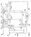
- the embodiment shown in Fig. 2 further comprises a device 11 for generating at least one Auxiliary power.
- the device 11 is in particular of Advantage, when the excitation current measured as accurately as possible and therefore should not be falsified. Exists between the auxiliary current and the excitation current a predetermined Related, so can both the current threshold and the charge threshold based on this auxiliary current be determined.
- the device 11 for generating at least one auxiliary current may include a current mirror 1101 with a first input 1103, a second input 1105 and a third input 1107 and an output 1109, which is connected to the mass M.
- the first entrance 1103 of the current mirror 1101 is connected to the output 97 of the transistor 91 connected so that in this first input of Excitation current flow into it and generate two auxiliary currents can, respectively, in the second input 1105 and in the flow in third input 1107.
- the auxiliary current flowing into the second input 1105 of the current mirror 1101 is used in the exemplary embodiment illustrated in FIG. 2 by the charge threshold value determining device 7.
- the device 7 further comprises a first comparator 71 having a first input 7101, a second input 7103 and an output 7105. To the input 7101, a predetermined reference voltage can be applied, which can be used to determine the charge threshold.
- the second input 7103 of the comparator 71 is connected via a capacitor 73 to a supply voltage source which supplies a supply voltage V DD .
- the comparator 71 now compares the two at the inputs 7101 and 7103 applied voltages and supplies its output 7105 is a result of this comparison. Is the voltage applied to the second input 7103 is greater than that which is applied to the first input 7101, so means this is that the capacity already has a certain amount of charge has received a charge threshold has exceeded.
- Capacity 73 replaced by any functionality can be, which has an integral behavior, such as for example, a suitably interconnected operational amplifier.
- Parallel to the capacitance 73 may further include a switch 75 with be connected to a control input 7501, which serves the capacitance 73 before a new emission process of the electron emission device to be discharged by bridging.
- the embodiment shown in FIG. 2 further includes a second comparator 51 having a first input 5101, a second input 5103 and an output 5105.
- a reference voltage can be applied to the input 5101, which can be used to determine the current threshold value.
- the second input of the comparator is connected in this embodiment, with the third input 1107 of the current mirror 1101, in which flows another auxiliary current having a predetermined relationship with the excitation current.
- the second input 5103 of the comparator 51 is further connected via a resistor to the voltage source, which supplies the voltage V DD .
- the auxiliary current flowing through this resistor causes a voltage which is applied to the second input 5103 and which is compared with the reference voltage applied to the first input 5101.
- this voltage is smaller than the reference voltage applied to the first input 5101, this means that the magnitude of the auxiliary current has fallen below a current threshold value represented by the voltage dropping across the resistor 53.
- the output 5105 of the comparator 51 is an output signal indicating the falling below the current threshold.
- the resistance 53 can be replaced by any functionality, which can convert a current into a voltage, such as a current controlled voltage source.
- Fig. 2 are the Outputs of the comparators 71 and 51 with the inputs 1301 and 1303 are connected to a logic 13, which further comprises a first Output 1305 and a second output 1307, connected.
- the logic 13 is designed such that the at their Inputs applied signals using a suitable Link, e.g. an OR link, combined or be evaluated and the result of this operation on first output 1305 is applied, which continues with the control input 9901 of the switch 99 is connected. Will the current threshold falls below or becomes the charge threshold exceeded, so the switch 99 due to the now first output 1305 of the logic 13 applied signal is closed, so that the transistor 91 in the blocking state goes over and turns off the excitation current.
- a suitable Link e.g. an OR link
- the two Output signals of the comparators 71 and 51 are in the Logic 13 also linked together so that the (high-voltage) transistor 91 is then opened when the dose, i.e. the amount of charge emitted has the correct value or the amount of current does not exceed the current threshold Has.
- the signal applied to the second output 1307 of the logic 13 signal is optional and can, for example, another parent Monitoring device to be supplied. This is especially advantageous when multiple electron emission devices 1 are arranged in an array, wherein each electron emission device is an inventive Control circuit may have. That at the second exit Signal applied 1307 to the logic 13 provides the identification feature, associated with each of the control circuits that is the electron emission device in the array, which forms a multi-electron emission device identified. With the help of this identification feature can the parent monitoring device now monitor a plurality of control circuits, for example when falling below the current threshold the disable control circuit concerned.
- Fig. 3 shows a further embodiment of the control circuit for controlling an electron emission device.
- this embodiment has a number of functionalities already having in the illustrated in Fig. 2 Embodiment are included in the following Functions with the same reference not yet once described.
- a current application device 15 which serves the so-called Counteract tactile penetration effect.
- This Effect is on a very fast, steep change of one Attributed to a node's potential, this change also with the neighboring knots to potential fluctuations during and just after the switching leads, indicating parasitic Coupling elements, such as. B. coupling capacity of the nodes, is due. It is the height and the duration the potential fluctuation by that through a neighboring knot co-determined with flowing electricity. In particular, this means in the case of de-energized nodes, which act on a current it comes to a particularly strong clock penetration.
- the current application device 15 comprises in this embodiment, a current source 1501, at the input of a voltage, for example, the voltage V DD is applied, which is connected in parallel to the transistor 91 such that a discharged from this current source Umladestrom the excitation current through the transistor 91 flows, is superimposed.
- This Umladestrom supplied by the current source 1501 is now used to transhipment of the aforementioned parasitic coupling capacitances, so that this is not a part of the excitation current is lost. This is particularly important during the turn-on of the device for switching off the excitation current 9, because in this case the switch 99 is opened and to the control input 93, a predetermined voltage is applied, so that the transistor 91 is now turned on and thus conductive.
- the through the current application device 15 in the Node 97 fed current thus serves the mentioned To recharge parasitic capacitances, so that when switching the device 9 whose stationary state is now sets faster.
- the realization the current application device 15 through the Current source 1501 only one of the possible embodiments represents.
- the Umladestrom be generated with the help of any functionality which can provide a transhipment current, such as a suitable connected current mirror or a voltage-controlled Power source.
- the embodiment shown in Fig. 3 includes Further, another current application device 17, the the means 7 for determining the charge threshold provides a further current, that of the of the current application device 15 supplied Umladestrom dependent is.
- the current application device 17 comprises a current source 1701 whose output is connected to node 7103 is and which is connected in parallel with the capacitor 73.
- the exemplary embodiment illustrated in FIG. 3 includes a further current application device 19 in order to supply a further current to the means for determining the current threshold value 5, which current is dependent on the charge-reversal current impressed by the current application device 15.
- the current application device 19 comprises a current source 1901 whose output is connected to the node 1503 and at whose input a voltage can be applied, for example the voltage V DD .
- the of the current application device 17 and of the Current applying device 19 supplied currents in addition, in the switched-on state of the shutdown device 9 the excitation current superimposed Umladestrom, the is impressed by the current application device 15, such that both the magnitude of the excitation current and the amount of charge emitted unadulterated and thus can be determined with sufficient accuracy.
- the entire electronic system is electrically grounded and operates with the voltage V DD to 5 V customary for IC technologies.
- the transistor 91 can be designed as a high-voltage transistor whose drain is at a significantly higher voltage than the positive supply voltage.
- the embodiments shown in Fig. 2 and in Fig. 3 may further comprise a control circuit, the is formed such that the to the control input 93 of the Transistor 91 applicable voltage acting as an input signal can be interpreted, the logic 13 resets.
- the charge of the capacitor is via a to the Control input 7501 of the switch 75 can be applied reset signal set to zero, the transistor 91 closed and the Comparator 51 turned on over a previously defined delay.
- the comparator 51 is only after a delay switched on so that the stationary excitation current is monitored.
- the comparator 51 first checks for the defined delay, whether a minimum excitation current flows.
- the comparator 71 monitors the voltage difference over the capacity 73 on the basis of the mirrored and integrated excitation current.
- the two output signals the comparators 51 and 71 are in logic 13 suitably evaluated and there will be a corresponding output signal (Out) derived for processing, that at the output 1307 is present.
- the switch 99 is then opened, so that no further excitation current through the transistor 91 and thus flows through an electron source.
- Array for controlling a multi-electron emission device comprises a plurality of electron emission devices, which are arranged in an array and either individually or when grouped into small groups are groups of the invention Control circuit to be controlled.
- the multi-electron emission device for example the CNT, that's the way it is important for a high resolution as well as for a quick Structure generation that of the CNT or of the CNT groups emitted amount of charge accurately metered can be. If the CNTs are defective, i. be either no electrons emitted or can the necessary amount of charge not reached within a time interval so the CNT must be turned off so no unfinished structure points emerge, resulting in a deactivation the control circuit and thus switching off the excitation current can be achieved.
- each in the electron emission device included in the multi-electron emission device an identification feature according to the invention, that clearly identifies them, such as one formed on the basis of the array coordinates Address.
- a superordinate monitoring device about their current operating status, for example whether the amount of the excitation current is a predetermined one Current threshold reached, can inform.
- the in Fig. 2 and embodiments of the invention shown in Fig. 3 comprise the logic 13, at the second output 1307th this information of the superior monitoring device is made available.
- the magnitude of the excitation current is the predetermined current threshold not, so provides the comparator of the invention 51 a corresponding output signal, so that after a suitable evaluation of the two output signals of the comparators 51 and 71 by the logic 13 a corresponding Signal at the output 1307 is applied, that of the parent Monitoring device indicates that the amount of current the current threshold falls below, so that the control circuit the corresponding electron emission device is deactivated.
Landscapes
- Engineering & Computer Science (AREA)
- Nanotechnology (AREA)
- Chemical & Material Sciences (AREA)
- Physics & Mathematics (AREA)
- Health & Medical Sciences (AREA)
- Mathematical Physics (AREA)
- Theoretical Computer Science (AREA)
- Toxicology (AREA)
- Crystallography & Structural Chemistry (AREA)
- General Health & Medical Sciences (AREA)
- Cold Cathode And The Manufacture (AREA)
- Electron Beam Exposure (AREA)
- Electron Sources, Ion Sources (AREA)
Description
- Fig. 1
- die erfindungsgemäße Steuerschaltung zum Steuern einer Elektronenemissionsvorrichtung;
- Fig. 2
- ein Ausführungsbeispiel der erfindungsgemäßen Steuerschaltung;
- Fig. 3
- ein weiteres Ausführungsbeispiel der erfindungsgemäßen Steuerschaltung; und
- Fig. 4a bis 4c
- eine Skizze der Spannungs- bzw. Potentialsituation zwischen Steuerschaltung, Carbon Nano Tube und zu belichtendem Substrat.
Fig. 2 zeigt ein bevorzugtes Ausführungsbeispiel der Erfindung, wobei die Einrichtung 9, die Einrichtung 5 sowie die Einrichtung 7 zum Feststellen des Ladungsschwellwerts gestrichelt markiert sind.
Claims (16)
- Steuerschaltung zum Steuern einer Elektronenemissionsvorrichtung, die ausgebildet ist, um bei einer angelegten Spannung einen Erregungsstrom aufzunehmen, der mit einer Anzahl von emittierten Elektronen zusammenhängt, mit folgenden Merkmalen:einer ersten Einrichtung (7) zum Feststellen, ob eine durch den Erregungsstrom transportierte Ladungsmenge einen vorbestimmten Ladungsschwellwert erreicht;einer zweiten Einrichtung (5) zum Feststellen, ob ein Betrag des Erregungsstroms einen vorbestimmten Stromschwellwert erreicht; undeiner Einrichtung (9) zum Abschalten des Erregungsstroms, sobald die erste Einrichtung (7) feststellt, daß die Ladungsmenge einen vorbestimmten Ladungsschwellwert erreicht hat, oder sobald die zweite Einrichtung (5) feststellt, daß der Betrag des Erregungsstroms kleiner als der vorbestimmte Stromschwellwert ist.
- Steuerschaltung gemäß Anspruch 1, die ferner folgendes Merkmal aufweist:eine Einrichtung (11) zum Erzeugen von zumindest einem Hilfsstrom, der in einem vorbestimmten Zusammenhang zu dem Erregungsstrom ist, und wobei die erste Einrichtung (7) und/oder die zweite Einrichtung (5) ausgebildet ist, um auf der Basis von zumindest einem Hilfsstrom zu arbeiten.
- Steuerschaltung gemäß Anspruch 1 oder 2, wobei die erste Einrichtung (7) folgende Merkmale aufweist:einen Komparator (71) mit einem ersten und einem zweiten Eingang und einem Ausgang, wobei an dem ersten Eingang eine Referenzspannung anliegt, die zur Bestimmung des Ladungsschwellwerts herangezogen wird; undeiner Kapazität (73) zur Aufnahme einer durch den Hilfsstrom transportierten Ladungsmenge, die proportional zu der durch den Erregungsstrom transportierten Ladungsmenge ist, die mit dem zweiten Eingang des Komparators und einer weiteren Spannungsquelle verbunden ist.
- Steuerschaltung gemäß Anspruch 3, die ferner einen steuerbaren Schalter (75) umfaßt, der parallel zu der Kapazität (73) geschaltet ist, der nach einer bestimmten Emissionszeit der Elektronenemissionsvorrichtung geschlossen werden kann, um diese Kapazität zu entladen.
- Steuerschaltung gemäß Anspruch 3 oder 4, wobei die zweite Einrichtung (5) folgende Merkmale aufweist:einen Komparator (51) mit einem ersten und einem zweiten Eingang, wobei an dem zweiten Eingang eine Referenzspannung anlegbar ist, die zur Bestimmung des Ladungsschwellwerts herangezogen wird;einen Strom-Spannungswandler (53), der mit einer Spannungsquelle und dem zweiten Eingang des Komparators (51) verbunden ist, der ausgebildet ist, um einen Hilfsstrom in eine Spannung umzuwandeln, die an den ersten Eingang des Komparators (51) anlegbar ist.
- Steuerschaltung gemäß Anspruch 5, wobei der Strom-Spannungswandler ein resistives Element ist.
- Steuerschaltung gemäß Anspruch 1, wobei die Einrichtung (9) zum Abschalten des Erregungsstroms folgendes Merkmal aufweist:einen Transistor (91) mit einem Steuereingang, einem Eingang und einem Ausgang, wobei an den Eingang eine Spannung anlegbar ist, deren Betrag einen für die Elektronenemission der Elektronenemissionsvorrichtung notwendigen Wert nicht unterschreitet.
- Steuerschaltung gemäß Anspruch 7, die eine Kapazität (C1) umfaßt, die zwischen dem Steuereingang des Transistors (91) und einer Masse verbunden ist, um eine angelegte Steuerspannung dauerhaft zu speichern.
- Steuerschaltung gemäß Anspruch 2 und 7,
wobei die Einrichtung (11) zum Erzeugen von mindestens einem Hilfsstrom einen Stromspiegel umfaßt mit einem ersten, einem zweiten und einem dritten Eingang und einem Ausgang, wobei der erste Eingang mit dem Ausgang des Transistors (91) verbunden ist;
wobei der zweite Eingang mit dem zweiten Eingang des Komparators (51) verbunden ist;
wobei der dritte Eingang mit dem zweiten Eingang des Komparators (71) verbunden ist; und
der ausgebildet ist, um in Abhängigkeit von einem in den ersten Eingang fließenden Strom einen ersten Hilfsstrom zu erzeugen, der in den zweiten Eingang fließt;
der ausgebildet ist, um in Abhängigkeit von dem in den ersten Eingang fließenden Strom einen zweiten Hilfsstrom zu erzeugen, der in den dritten Eingang fließt;
wobei der Ausgang mit einer Masse verbunden ist. - Steuerschaltung gemäß einem der vorhergehenden Ansprüche, die eine Logikschaltung (13) umfaßt, die ausgebildet ist, um ein Ausgangssignal der zweiten Einrichtung (5) zum Feststellen des Stormschwellenwerts und ein Ausgangssignal der ersten Einrichtung (7) zum Feststellen des Ladungsschwellwerts mit einer ODER-Verknüpfung zu kombinieren, und um das Ergebnis dieser ODER-Verknüpfung der Einrichtung (9) zum Abschalten des Erregungsstroms zur Verfügung zu stellen.
- Steuerschaltung gemäß Anspruch 10, die ferner ausgebildet ist, um das Ergebnis der ODER-Verknüpfung zusammen mit einem Identifikationsmerkmal der Steuerschaltung einer übergeordneten Überwachungseinrichtung zur Verfügung zu stellen.
- Steuerschaltung gemäß einem der vorhergehenden Ansprüche, bei der die Einrichtung (9) zum Abschalten des Erregungsstroms einen ersten und einen zweiten Knoten aufweist, wobei der erste Knoten mit einer angelegten Spannung verbindbar ist, und wobei zwischen dem ersten und dem zweiten Knoten durch eine Einschaltung eine leitende Verbindung herstellbar ist, wobei der zweite Knoten mit einer Strombeaufschlagungseinrichtung (15) verbunden ist, die ausgebildet ist, um einen Umladestrom bei einem ausgeschalteten Zustand der Einrichtung (9) zum Abschalten des Erregungsstroms in den zweiten Knoten einzuspeisen.
- Steuerschaltung gemäß Anspruch 12, die ferner eine Strombeaufschlagungseinrichtung (17) umfaßt, die ausgebildet ist, um der ersten Einrichtung (7) zum Feststellen des Ladungsschwellwerts einen von dem Umladestrom abhängigen Strom zuzuführen bei einem eingeschalteten Zustand der Einrichtung (9) zum Abschalten des Erregungsstroms.
- Steuerschaltung gemäß Anspruch 12, die ferner eine Strombeaufschlagungsvorrichtung (19) umfaßt, die ausgebildet ist, um der zweiten Einrichtung zum Feststellen des Stromschwellwerts einen von dem Umladestrom abhängigen Strom zuzuführen bei einem eingeschalteten Zustand der Einrichtung (9) zum Abschalten des Erregungsstroms.
- Verfahren zum Steuern einer Elektronenemissionsvorrichtung, die ausgebildet ist, um bei einer angelegten Spannung einen Erregungsstrom aufzunehmen, der mit einer Anzahl von emittierten Elektronen zusammenhängt, mit folgenden Schritten:Feststellen (7), ob eine durch den Erregungsstrom transportierte Ladungsmenge einen vorbestimmten Ladungsschwellwert erreicht;Feststellen (5), ob ein Betrag des Erregungsstroms einen vorbestimmten Stromschwellwert erreicht; undAbschalten (9) des Erregungsstroms, sobald festgestellt wird, daß die Ladungsmenge einen vorbestimmten Ladungsschwellwert erreicht hat, oder sobald festgestellt wird, daß der Betrag des Erregungsstroms kleiner als der vorbestimmte Stromschwellwert ist.
- Array zum Steuern einer Multielektronenemissionsvorrichtung, wobei die Multielektronenemissionsvorrichtung eine Mehrzahl von Elektronenemissionsvorrichtungen aufweist, mit folgenden Merkmalen:wobei jeder Steuerschaltung ein Identifikationsmerkmal zugeordnet ist, das die Elektronenemissionsvorrichtung in diesem Array eindeutig identifiziert; undeiner Mehrzahl von Steuerschaltungen gemäß einem der Ansprüche 1 bis 9, wobei eine Steuerschaltung für eine Elektronenemissionsvorrichtung vorgesehen ist;
eine Überwachungseinrichtung zum Überwachen der Mehrzahl von Steuerschaltungen, die ausgebildet ist, um zu erfassen, ob bei einer Steuerschaltung der Betrag des Erregungsstroms einen vorbestimmten Schwellenwert erreicht;
wobei die Überwachungseinrichtung ausgebildet ist, um eine dauerhafte Deaktivierung der Steuerschaltung auf der Basis des Identifikationsmerkmals zu bewirken.
Applications Claiming Priority (5)
| Application Number | Priority Date | Filing Date | Title |
|---|---|---|---|
| DE10240885 | 2002-09-04 | ||
| DE10240885 | 2002-09-04 | ||
| DE10241433 | 2002-09-06 | ||
| DE10241433A DE10241433B4 (de) | 2002-09-04 | 2002-09-06 | Steuerschaltung zum Steuern einer Elektronenemissionsvorrichtung |
| PCT/EP2003/009486 WO2004030422A1 (de) | 2002-09-04 | 2003-08-27 | Steuerschaltung zum steuern einer elektronenemissionsvorrichtung |
Publications (3)
| Publication Number | Publication Date |
|---|---|
| EP1522211A1 EP1522211A1 (de) | 2005-04-13 |
| EP1522211B1 true EP1522211B1 (de) | 2005-11-23 |
| EP1522211B8 EP1522211B8 (de) | 2007-02-14 |
Family
ID=32043945
Family Applications (1)
| Application Number | Title | Priority Date | Filing Date |
|---|---|---|---|
| EP03798135A Expired - Lifetime EP1522211B8 (de) | 2002-09-04 | 2003-08-27 | Steuerschaltung zum steuern einer elektronenemissionsvorrichtung |
Country Status (5)
| Country | Link |
|---|---|
| US (1) | US7095186B2 (de) |
| EP (1) | EP1522211B8 (de) |
| JP (1) | JP2006516175A (de) |
| AT (1) | ATE311090T1 (de) |
| WO (1) | WO2004030422A1 (de) |
Families Citing this family (1)
| Publication number | Priority date | Publication date | Assignee | Title |
|---|---|---|---|---|
| US10262829B2 (en) * | 2015-12-14 | 2019-04-16 | General Electric Company | Protection circuit assembly and method for high voltage systems |
Family Cites Families (12)
| Publication number | Priority date | Publication date | Assignee | Title |
|---|---|---|---|---|
| JPS5342695A (en) * | 1976-09-30 | 1978-04-18 | Toshiba Corp | Ct scanner |
| US4990766A (en) * | 1989-05-22 | 1991-02-05 | Murasa International | Solid state electron amplifier |
| JPH03210798A (ja) * | 1990-01-12 | 1991-09-13 | Toshiba Corp | X線診断装置 |
| US6204834B1 (en) * | 1994-08-17 | 2001-03-20 | Si Diamond Technology, Inc. | System and method for achieving uniform screen brightness within a matrix display |
| FR2730843B1 (fr) * | 1995-02-17 | 1997-05-09 | Pixtech Sa | Dispositif d'adressage d'une electrode d'ecran plat de visualisation a micropointes |
| US5656892A (en) * | 1995-11-17 | 1997-08-12 | Micron Display Technology, Inc. | Field emission display having emitter control with current sensing feedback |
| KR100230077B1 (ko) * | 1995-11-30 | 1999-11-15 | 김영남 | 전계 방출 표시기의 셀 구동장치 |
| US6498349B1 (en) * | 1997-02-05 | 2002-12-24 | Ut-Battelle | Electrostatically focused addressable field emission array chips (AFEA's) for high-speed massively parallel maskless digital E-beam direct write lithography and scanning electron microscopy |
| US5982082A (en) * | 1997-05-06 | 1999-11-09 | St. Clair Intellectual Property Consultants, Inc. | Field emission display devices |
| AU2987699A (en) * | 1998-03-06 | 1999-09-20 | Xrt Corp. | Method and x-ray device using adaptable power source |
| US6392355B1 (en) * | 2000-04-25 | 2002-05-21 | Mcnc | Closed-loop cold cathode current regulator |
| EP1274111B1 (de) * | 2001-07-06 | 2005-09-07 | ICT, Integrated Circuit Testing GmbH | Elektronenemissionsvorrichtung |
-
2003
- 2003-08-27 EP EP03798135A patent/EP1522211B8/de not_active Expired - Lifetime
- 2003-08-27 AT AT03798135T patent/ATE311090T1/de not_active IP Right Cessation
- 2003-08-27 WO PCT/EP2003/009486 patent/WO2004030422A1/de not_active Ceased
- 2003-08-27 JP JP2004538844A patent/JP2006516175A/ja active Pending
-
2005
- 2005-03-01 US US11/070,741 patent/US7095186B2/en not_active Expired - Lifetime
Also Published As
| Publication number | Publication date |
|---|---|
| ATE311090T1 (de) | 2005-12-15 |
| EP1522211A1 (de) | 2005-04-13 |
| WO2004030422A1 (de) | 2004-04-08 |
| US7095186B2 (en) | 2006-08-22 |
| US20050147148A1 (en) | 2005-07-07 |
| EP1522211B8 (de) | 2007-02-14 |
| JP2006516175A (ja) | 2006-06-22 |
Similar Documents
| Publication | Publication Date | Title |
|---|---|---|
| DE3710865C2 (de) | ||
| DE69209981T2 (de) | Elektrostatische Elektronenstrahl-Fokussierungseinrichtung für eine Feldemissionsvorrichtung | |
| EP3861565A1 (de) | Vielstrahl-teilchenstrahlsystem und verfahren zum betreiben eines solchen | |
| DE4037206A1 (de) | Quellspannungssteuerschaltkreis | |
| DE2011794C3 (de) | Halbleiterspeicheranordnung | |
| DE102005036555A1 (de) | Programmieren programmierbarer resistiver Speichervorrichtungen | |
| DE2819195C2 (de) | Schaltungsanordnung zum Betreiben einer Linienkathode in einem Bildwiedergabegerät | |
| DE2528741C2 (de) | Matrixmodul | |
| DE1283891B (de) | Elektronische Schaltungsanordnung zum Ein- und Ausschalten einer Nutzsignal-UEbertragung | |
| EP0648019B1 (de) | CMOS-Schaltung mit erhöhter Spannungsfestigkeit | |
| EP0689058A2 (de) | Schaltungsanordnung zum Überwachen eines Schaltungspunktes auf einen Leckwiderstand | |
| DE4017617A1 (de) | Spannungserzeugungsschaltkreis fuer halbleitereinrichtungen | |
| DE3730440A1 (de) | Lineare spannungsregelung fuer eine solarzellenanordnung | |
| DE2221138A1 (de) | Feldemissions-Elektronenkanone | |
| EP1522211B1 (de) | Steuerschaltung zum steuern einer elektronenemissionsvorrichtung | |
| EP0944159B1 (de) | Gleichspannungswandler | |
| DE2232274C2 (de) | Statischer Halbleiterspeicher mit Feldeffekttransistoren | |
| DE10241433B4 (de) | Steuerschaltung zum Steuern einer Elektronenemissionsvorrichtung | |
| DE19746113A1 (de) | Spannungsversorgungsschaltung | |
| DE102021106815B4 (de) | Stromversorgungsgenerator und betriebsverfahren dafür | |
| DE4020187A1 (de) | Ansteuerschaltung fuer eine transistorvorrichtung | |
| DE1135038B (de) | Bistabile Kippanordnung mit Tunneldioden und Schalttransistoren | |
| DE10134557A1 (de) | Schaltungsanordnung und Verfahren zum Entladen mindestens eines Schaltungsknotens | |
| DE10117362A1 (de) | Zufallszahlengenerator und Verfahren zum Erzeugen einer Zufallszahl | |
| DE2525097C3 (de) | Verfahren zum Betrieb eines n-Kanal-Speicher-FET |
Legal Events
| Date | Code | Title | Description |
|---|---|---|---|
| PUAI | Public reference made under article 153(3) epc to a published international application that has entered the european phase |
Free format text: ORIGINAL CODE: 0009012 |
|
| 17P | Request for examination filed |
Effective date: 20050207 |
|
| AK | Designated contracting states |
Kind code of ref document: A1 Designated state(s): AT BE BG CH CY CZ DE DK EE ES FI FR GB GR HU IE IT LI LU MC NL PT RO SE SI SK TR |
|
| GRAP | Despatch of communication of intention to grant a patent |
Free format text: ORIGINAL CODE: EPIDOSNIGR1 |
|
| GRAS | Grant fee paid |
Free format text: ORIGINAL CODE: EPIDOSNIGR3 |
|
| GRAA | (expected) grant |
Free format text: ORIGINAL CODE: 0009210 |
|
| AK | Designated contracting states |
Kind code of ref document: B1 Designated state(s): AT BE BG CH CY CZ DE DK EE ES FI FR GB GR HU IE IT LI LU MC NL PT RO SE SI SK TR |
|
| REG | Reference to a national code |
Ref country code: GB Ref legal event code: FG4D Free format text: NOT ENGLISH |
|
| REG | Reference to a national code |
Ref country code: CH Ref legal event code: EP |
|
| REG | Reference to a national code |
Ref country code: CH Ref legal event code: PK Free format text: DIE BENENNUNG CH/LI WURDE VOR ERTEILUNG ZURUECKGENOMMEN. |
|
| RBV | Designated contracting states (corrected) |
Designated state(s): FR GB NL |
|
| REG | Reference to a national code |
Ref country code: IE Ref legal event code: FG4D Free format text: LANGUAGE OF EP DOCUMENT: GERMAN |
|
| REG | Reference to a national code |
Ref country code: DE Ref legal event code: 8566 |
|
| GBT | Gb: translation of ep patent filed (gb section 77(6)(a)/1977) |
Effective date: 20060123 |
|
| ET | Fr: translation filed | ||
| REG | Reference to a national code |
Ref country code: IE Ref legal event code: FD4D |
|
| PLBE | No opposition filed within time limit |
Free format text: ORIGINAL CODE: 0009261 |
|
| STAA | Information on the status of an ep patent application or granted ep patent |
Free format text: STATUS: NO OPPOSITION FILED WITHIN TIME LIMIT |
|
| 26N | No opposition filed |
Effective date: 20060824 |
|
| BERE | Be: lapsed |
Owner name: FRAUNHOFER-GESELLSCHAFT ZUR FORDERUNG DER ANGEWAN Effective date: 20060831 |
|
| REG | Reference to a national code |
Ref country code: FR Ref legal event code: PLFP Year of fee payment: 14 |
|
| REG | Reference to a national code |
Ref country code: FR Ref legal event code: PLFP Year of fee payment: 15 |
|
| REG | Reference to a national code |
Ref country code: FR Ref legal event code: PLFP Year of fee payment: 16 |
|
| PGFP | Annual fee paid to national office [announced via postgrant information from national office to epo] |
Ref country code: NL Payment date: 20220822 Year of fee payment: 20 |
|
| PGFP | Annual fee paid to national office [announced via postgrant information from national office to epo] |
Ref country code: GB Payment date: 20220824 Year of fee payment: 20 |
|
| PGFP | Annual fee paid to national office [announced via postgrant information from national office to epo] |
Ref country code: FR Payment date: 20220822 Year of fee payment: 20 |
|
| P01 | Opt-out of the competence of the unified patent court (upc) registered |
Effective date: 20230524 |
|
| REG | Reference to a national code |
Ref country code: NL Ref legal event code: MK Effective date: 20230826 |
|
| REG | Reference to a national code |
Ref country code: GB Ref legal event code: PE20 Expiry date: 20230826 |
|
| PG25 | Lapsed in a contracting state [announced via postgrant information from national office to epo] |
Ref country code: GB Free format text: LAPSE BECAUSE OF EXPIRATION OF PROTECTION Effective date: 20230826 |