EP1522092B1 - Composant a semiconducteur pourvu d'une couche semiconductrice absorbant les contraintes et procede de fabrication correspondant - Google Patents
Composant a semiconducteur pourvu d'une couche semiconductrice absorbant les contraintes et procede de fabrication correspondant Download PDFInfo
- Publication number
- EP1522092B1 EP1522092B1 EP03764890A EP03764890A EP1522092B1 EP 1522092 B1 EP1522092 B1 EP 1522092B1 EP 03764890 A EP03764890 A EP 03764890A EP 03764890 A EP03764890 A EP 03764890A EP 1522092 B1 EP1522092 B1 EP 1522092B1
- Authority
- EP
- European Patent Office
- Prior art keywords
- layer
- lattice constant
- semiconductor
- stress
- gate dielectric
- Prior art date
- Legal status (The legal status is an assumption and is not a legal conclusion. Google has not performed a legal analysis and makes no representation as to the accuracy of the status listed.)
- Expired - Lifetime
Links
Images

Classifications
-
- H—ELECTRICITY
- H10—SEMICONDUCTOR DEVICES; ELECTRIC SOLID-STATE DEVICES NOT OTHERWISE PROVIDED FOR
- H10P—GENERIC PROCESSES OR APPARATUS FOR THE MANUFACTURE OR TREATMENT OF DEVICES COVERED BY CLASS H10
- H10P14/00—Formation of materials, e.g. in the shape of layers or pillars
- H10P14/60—Formation of materials, e.g. in the shape of layers or pillars of insulating materials
- H10P14/63—Formation of materials, e.g. in the shape of layers or pillars of insulating materials characterised by the formation processes
- H10P14/6326—Deposition processes
- H10P14/6328—Deposition from the gas or vapour phase
- H10P14/6334—Deposition from the gas or vapour phase using decomposition or reaction of gaseous or vapour phase compounds, i.e. chemical vapour deposition
- H10P14/6339—Deposition from the gas or vapour phase using decomposition or reaction of gaseous or vapour phase compounds, i.e. chemical vapour deposition deposition by cyclic CVD, e.g. ALD, ALE or pulsed CVD
-
- H—ELECTRICITY
- H10—SEMICONDUCTOR DEVICES; ELECTRIC SOLID-STATE DEVICES NOT OTHERWISE PROVIDED FOR
- H10D—INORGANIC ELECTRIC SEMICONDUCTOR DEVICES
- H10D30/00—Field-effect transistors [FET]
- H10D30/01—Manufacture or treatment
- H10D30/021—Manufacture or treatment of FETs having insulated gates [IGFET]
- H10D30/031—Manufacture or treatment of FETs having insulated gates [IGFET] of thin-film transistors [TFT]
- H10D30/0321—Manufacture or treatment of FETs having insulated gates [IGFET] of thin-film transistors [TFT] comprising silicon, e.g. amorphous silicon or polysilicon
- H10D30/0323—Manufacture or treatment of FETs having insulated gates [IGFET] of thin-film transistors [TFT] comprising silicon, e.g. amorphous silicon or polysilicon comprising monocrystalline silicon
- H10D30/0327—Manufacture or treatment of FETs having insulated gates [IGFET] of thin-film transistors [TFT] comprising silicon, e.g. amorphous silicon or polysilicon comprising monocrystalline silicon on sapphire substrates, e.g. of silicon-on-sapphire [SOS] transistor
-
- H—ELECTRICITY
- H10—SEMICONDUCTOR DEVICES; ELECTRIC SOLID-STATE DEVICES NOT OTHERWISE PROVIDED FOR
- H10D—INORGANIC ELECTRIC SEMICONDUCTOR DEVICES
- H10D30/00—Field-effect transistors [FET]
- H10D30/60—Insulated-gate field-effect transistors [IGFET]
- H10D30/67—Thin-film transistors [TFT]
- H10D30/674—Thin-film transistors [TFT] characterised by the active materials
- H10D30/6741—Group IV materials, e.g. germanium or silicon carbide
- H10D30/6743—Silicon
- H10D30/6744—Monocrystalline silicon
-
- H—ELECTRICITY
- H10—SEMICONDUCTOR DEVICES; ELECTRIC SOLID-STATE DEVICES NOT OTHERWISE PROVIDED FOR
- H10D—INORGANIC ELECTRIC SEMICONDUCTOR DEVICES
- H10D30/00—Field-effect transistors [FET]
- H10D30/60—Insulated-gate field-effect transistors [IGFET]
- H10D30/67—Thin-film transistors [TFT]
- H10D30/6758—Thin-film transistors [TFT] characterised by the insulating substrates
-
- H—ELECTRICITY
- H10—SEMICONDUCTOR DEVICES; ELECTRIC SOLID-STATE DEVICES NOT OTHERWISE PROVIDED FOR
- H10D—INORGANIC ELECTRIC SEMICONDUCTOR DEVICES
- H10D30/00—Field-effect transistors [FET]
- H10D30/60—Insulated-gate field-effect transistors [IGFET]
- H10D30/751—Insulated-gate field-effect transistors [IGFET] having composition variations in the channel regions
-
- H—ELECTRICITY
- H10—SEMICONDUCTOR DEVICES; ELECTRIC SOLID-STATE DEVICES NOT OTHERWISE PROVIDED FOR
- H10D—INORGANIC ELECTRIC SEMICONDUCTOR DEVICES
- H10D30/00—Field-effect transistors [FET]
- H10D30/60—Insulated-gate field-effect transistors [IGFET]
- H10D30/791—Arrangements for exerting mechanical stress on the crystal lattice of the channel regions
- H10D30/798—Arrangements for exerting mechanical stress on the crystal lattice of the channel regions being provided in or under the channel regions
-
- H—ELECTRICITY
- H10—SEMICONDUCTOR DEVICES; ELECTRIC SOLID-STATE DEVICES NOT OTHERWISE PROVIDED FOR
- H10D—INORGANIC ELECTRIC SEMICONDUCTOR DEVICES
- H10D64/00—Electrodes of devices having potential barriers
- H10D64/01—Manufacture or treatment
- H10D64/013—Manufacture or treatment of electrodes having a conductor capacitively coupled to a semiconductor by an insulator
- H10D64/01302—Manufacture or treatment of electrodes having a conductor capacitively coupled to a semiconductor by an insulator the insulator being formed after the semiconductor body, the semiconductor being silicon
- H10D64/01332—Making the insulator
- H10D64/01336—Making the insulator on single crystalline silicon, e.g. chemical oxidation using a liquid
- H10D64/01342—Making the insulator on single crystalline silicon, e.g. chemical oxidation using a liquid by deposition, e.g. evaporation, ALD or laser deposition
-
- H—ELECTRICITY
- H10—SEMICONDUCTOR DEVICES; ELECTRIC SOLID-STATE DEVICES NOT OTHERWISE PROVIDED FOR
- H10P—GENERIC PROCESSES OR APPARATUS FOR THE MANUFACTURE OR TREATMENT OF DEVICES COVERED BY CLASS H10
- H10P14/00—Formation of materials, e.g. in the shape of layers or pillars
- H10P14/20—Formation of materials, e.g. in the shape of layers or pillars of semiconductor materials
- H10P14/29—Formation of materials, e.g. in the shape of layers or pillars of semiconductor materials characterised by the substrates
- H10P14/2901—Materials
- H10P14/2902—Materials being Group IVA materials
- H10P14/2905—Silicon, silicon germanium or germanium
-
- H—ELECTRICITY
- H10—SEMICONDUCTOR DEVICES; ELECTRIC SOLID-STATE DEVICES NOT OTHERWISE PROVIDED FOR
- H10P—GENERIC PROCESSES OR APPARATUS FOR THE MANUFACTURE OR TREATMENT OF DEVICES COVERED BY CLASS H10
- H10P14/00—Formation of materials, e.g. in the shape of layers or pillars
- H10P14/20—Formation of materials, e.g. in the shape of layers or pillars of semiconductor materials
- H10P14/32—Formation of materials, e.g. in the shape of layers or pillars of semiconductor materials characterised by intermediate layers between substrates and deposited layers
- H10P14/3202—Materials thereof
- H10P14/3238—Materials thereof being insulating materials
-
- H—ELECTRICITY
- H10—SEMICONDUCTOR DEVICES; ELECTRIC SOLID-STATE DEVICES NOT OTHERWISE PROVIDED FOR
- H10P—GENERIC PROCESSES OR APPARATUS FOR THE MANUFACTURE OR TREATMENT OF DEVICES COVERED BY CLASS H10
- H10P14/00—Formation of materials, e.g. in the shape of layers or pillars
- H10P14/20—Formation of materials, e.g. in the shape of layers or pillars of semiconductor materials
- H10P14/34—Deposited materials, e.g. layers
- H10P14/3402—Deposited materials, e.g. layers characterised by the chemical composition
- H10P14/3404—Deposited materials, e.g. layers characterised by the chemical composition being Group IVA materials
- H10P14/3411—Silicon, silicon germanium or germanium
-
- H—ELECTRICITY
- H10—SEMICONDUCTOR DEVICES; ELECTRIC SOLID-STATE DEVICES NOT OTHERWISE PROVIDED FOR
- H10P—GENERIC PROCESSES OR APPARATUS FOR THE MANUFACTURE OR TREATMENT OF DEVICES COVERED BY CLASS H10
- H10P14/00—Formation of materials, e.g. in the shape of layers or pillars
- H10P14/60—Formation of materials, e.g. in the shape of layers or pillars of insulating materials
- H10P14/63—Formation of materials, e.g. in the shape of layers or pillars of insulating materials characterised by the formation processes
- H10P14/6326—Deposition processes
- H10P14/6328—Deposition from the gas or vapour phase
- H10P14/6332—Deposition from the gas or vapour phase using thermal evaporation
-
- H—ELECTRICITY
- H10—SEMICONDUCTOR DEVICES; ELECTRIC SOLID-STATE DEVICES NOT OTHERWISE PROVIDED FOR
- H10P—GENERIC PROCESSES OR APPARATUS FOR THE MANUFACTURE OR TREATMENT OF DEVICES COVERED BY CLASS H10
- H10P14/00—Formation of materials, e.g. in the shape of layers or pillars
- H10P14/60—Formation of materials, e.g. in the shape of layers or pillars of insulating materials
- H10P14/63—Formation of materials, e.g. in the shape of layers or pillars of insulating materials characterised by the formation processes
- H10P14/6326—Deposition processes
- H10P14/6328—Deposition from the gas or vapour phase
- H10P14/6334—Deposition from the gas or vapour phase using decomposition or reaction of gaseous or vapour phase compounds, i.e. chemical vapour deposition
-
- H—ELECTRICITY
- H10—SEMICONDUCTOR DEVICES; ELECTRIC SOLID-STATE DEVICES NOT OTHERWISE PROVIDED FOR
- H10P—GENERIC PROCESSES OR APPARATUS FOR THE MANUFACTURE OR TREATMENT OF DEVICES COVERED BY CLASS H10
- H10P14/00—Formation of materials, e.g. in the shape of layers or pillars
- H10P14/60—Formation of materials, e.g. in the shape of layers or pillars of insulating materials
- H10P14/66—Formation of materials, e.g. in the shape of layers or pillars of insulating materials characterised by the type of materials
- H10P14/662—Laminate layers, e.g. stacks of alternating high-k metal oxides
-
- H—ELECTRICITY
- H10—SEMICONDUCTOR DEVICES; ELECTRIC SOLID-STATE DEVICES NOT OTHERWISE PROVIDED FOR
- H10P—GENERIC PROCESSES OR APPARATUS FOR THE MANUFACTURE OR TREATMENT OF DEVICES COVERED BY CLASS H10
- H10P14/00—Formation of materials, e.g. in the shape of layers or pillars
- H10P14/60—Formation of materials, e.g. in the shape of layers or pillars of insulating materials
- H10P14/69—Inorganic materials
- H10P14/692—Inorganic materials composed of oxides, glassy oxides or oxide-based glasses
- H10P14/6921—Inorganic materials composed of oxides, glassy oxides or oxide-based glasses containing silicon
- H10P14/69215—Inorganic materials composed of oxides, glassy oxides or oxide-based glasses containing silicon the material being a silicon oxide, e.g. SiO2
-
- H—ELECTRICITY
- H10—SEMICONDUCTOR DEVICES; ELECTRIC SOLID-STATE DEVICES NOT OTHERWISE PROVIDED FOR
- H10P—GENERIC PROCESSES OR APPARATUS FOR THE MANUFACTURE OR TREATMENT OF DEVICES COVERED BY CLASS H10
- H10P14/00—Formation of materials, e.g. in the shape of layers or pillars
- H10P14/60—Formation of materials, e.g. in the shape of layers or pillars of insulating materials
- H10P14/69—Inorganic materials
- H10P14/692—Inorganic materials composed of oxides, glassy oxides or oxide-based glasses
- H10P14/6921—Inorganic materials composed of oxides, glassy oxides or oxide-based glasses containing silicon
- H10P14/6928—Inorganic materials composed of oxides, glassy oxides or oxide-based glasses containing silicon the material containing silicon and at least one metal element, e.g. metal silicate based insulators or metal silicon oxynitrides
- H10P14/693—Inorganic materials composed of oxides, glassy oxides or oxide-based glasses containing silicon the material containing silicon and at least one metal element, e.g. metal silicate based insulators or metal silicon oxynitrides the material containing hafnium, e.g. HfSiOx or HfSiON
-
- H—ELECTRICITY
- H10—SEMICONDUCTOR DEVICES; ELECTRIC SOLID-STATE DEVICES NOT OTHERWISE PROVIDED FOR
- H10P—GENERIC PROCESSES OR APPARATUS FOR THE MANUFACTURE OR TREATMENT OF DEVICES COVERED BY CLASS H10
- H10P14/00—Formation of materials, e.g. in the shape of layers or pillars
- H10P14/60—Formation of materials, e.g. in the shape of layers or pillars of insulating materials
- H10P14/69—Inorganic materials
- H10P14/692—Inorganic materials composed of oxides, glassy oxides or oxide-based glasses
- H10P14/6938—Inorganic materials composed of oxides, glassy oxides or oxide-based glasses the material containing at least one metal element, e.g. metal oxides, metal oxynitrides or metal oxycarbides
- H10P14/6939—Inorganic materials composed of oxides, glassy oxides or oxide-based glasses the material containing at least one metal element, e.g. metal oxides, metal oxynitrides or metal oxycarbides characterised by the metal
-
- H—ELECTRICITY
- H10—SEMICONDUCTOR DEVICES; ELECTRIC SOLID-STATE DEVICES NOT OTHERWISE PROVIDED FOR
- H10P—GENERIC PROCESSES OR APPARATUS FOR THE MANUFACTURE OR TREATMENT OF DEVICES COVERED BY CLASS H10
- H10P14/00—Formation of materials, e.g. in the shape of layers or pillars
- H10P14/60—Formation of materials, e.g. in the shape of layers or pillars of insulating materials
- H10P14/69—Inorganic materials
- H10P14/694—Inorganic materials composed of nitrides
- H10P14/6943—Inorganic materials composed of nitrides containing silicon
- H10P14/69433—Inorganic materials composed of nitrides containing silicon the material being a silicon nitride not containing oxygen, e.g. SixNy or SixByNz
-
- H—ELECTRICITY
- H10—SEMICONDUCTOR DEVICES; ELECTRIC SOLID-STATE DEVICES NOT OTHERWISE PROVIDED FOR
- H10P—GENERIC PROCESSES OR APPARATUS FOR THE MANUFACTURE OR TREATMENT OF DEVICES COVERED BY CLASS H10
- H10P90/00—Preparation of wafers not covered by a single main group of this subclass, e.g. wafer reinforcement
- H10P90/19—Preparing inhomogeneous wafers
- H10P90/1904—Preparing vertically inhomogeneous wafers
- H10P90/1906—Preparing SOI wafers
-
- H—ELECTRICITY
- H10—SEMICONDUCTOR DEVICES; ELECTRIC SOLID-STATE DEVICES NOT OTHERWISE PROVIDED FOR
- H10W—GENERIC PACKAGES, INTERCONNECTIONS, CONNECTORS OR OTHER CONSTRUCTIONAL DETAILS OF DEVICES COVERED BY CLASS H10
- H10W10/00—Isolation regions in semiconductor bodies between components of integrated devices
- H10W10/10—Isolation regions comprising dielectric materials
- H10W10/181—Semiconductor-on-insulator [SOI] isolation regions, e.g. buried oxide regions of SOI wafers
-
- H—ELECTRICITY
- H10—SEMICONDUCTOR DEVICES; ELECTRIC SOLID-STATE DEVICES NOT OTHERWISE PROVIDED FOR
- H10D—INORGANIC ELECTRIC SEMICONDUCTOR DEVICES
- H10D30/00—Field-effect transistors [FET]
- H10D30/60—Insulated-gate field-effect transistors [IGFET]
- H10D30/67—Thin-film transistors [TFT]
- H10D30/6758—Thin-film transistors [TFT] characterised by the insulating substrates
- H10D30/6759—Silicon-on-sapphire [SOS] substrates
-
- H—ELECTRICITY
- H10—SEMICONDUCTOR DEVICES; ELECTRIC SOLID-STATE DEVICES NOT OTHERWISE PROVIDED FOR
- H10D—INORGANIC ELECTRIC SEMICONDUCTOR DEVICES
- H10D64/00—Electrodes of devices having potential barriers
- H10D64/01—Manufacture or treatment
- H10D64/013—Manufacture or treatment of electrodes having a conductor capacitively coupled to a semiconductor by an insulator
- H10D64/01302—Manufacture or treatment of electrodes having a conductor capacitively coupled to a semiconductor by an insulator the insulator being formed after the semiconductor body, the semiconductor being silicon
- H10D64/01332—Making the insulator
- H10D64/01336—Making the insulator on single crystalline silicon, e.g. chemical oxidation using a liquid
-
- H—ELECTRICITY
- H10—SEMICONDUCTOR DEVICES; ELECTRIC SOLID-STATE DEVICES NOT OTHERWISE PROVIDED FOR
- H10D—INORGANIC ELECTRIC SEMICONDUCTOR DEVICES
- H10D64/00—Electrodes of devices having potential barriers
- H10D64/60—Electrodes characterised by their materials
- H10D64/66—Electrodes having a conductor capacitively coupled to a semiconductor by an insulator, e.g. MIS electrodes
- H10D64/68—Electrodes having a conductor capacitively coupled to a semiconductor by an insulator, e.g. MIS electrodes characterised by the insulator, e.g. by the gate insulator
- H10D64/691—Electrodes having a conductor capacitively coupled to a semiconductor by an insulator, e.g. MIS electrodes characterised by the insulator, e.g. by the gate insulator comprising metallic compounds, e.g. metal oxides or metal silicates
-
- H—ELECTRICITY
- H10—SEMICONDUCTOR DEVICES; ELECTRIC SOLID-STATE DEVICES NOT OTHERWISE PROVIDED FOR
- H10D—INORGANIC ELECTRIC SEMICONDUCTOR DEVICES
- H10D64/00—Electrodes of devices having potential barriers
- H10D64/60—Electrodes characterised by their materials
- H10D64/66—Electrodes having a conductor capacitively coupled to a semiconductor by an insulator, e.g. MIS electrodes
- H10D64/68—Electrodes having a conductor capacitively coupled to a semiconductor by an insulator, e.g. MIS electrodes characterised by the insulator, e.g. by the gate insulator
- H10D64/693—Electrodes having a conductor capacitively coupled to a semiconductor by an insulator, e.g. MIS electrodes characterised by the insulator, e.g. by the gate insulator the insulator comprising nitrogen, e.g. nitrides, oxynitrides or nitrogen-doped materials
-
- H—ELECTRICITY
- H10—SEMICONDUCTOR DEVICES; ELECTRIC SOLID-STATE DEVICES NOT OTHERWISE PROVIDED FOR
- H10P—GENERIC PROCESSES OR APPARATUS FOR THE MANUFACTURE OR TREATMENT OF DEVICES COVERED BY CLASS H10
- H10P14/00—Formation of materials, e.g. in the shape of layers or pillars
- H10P14/20—Formation of materials, e.g. in the shape of layers or pillars of semiconductor materials
- H10P14/32—Formation of materials, e.g. in the shape of layers or pillars of semiconductor materials characterised by intermediate layers between substrates and deposited layers
- H10P14/3202—Materials thereof
- H10P14/3204—Materials thereof being Group IVA semiconducting materials
- H10P14/3211—Silicon, silicon germanium or germanium
-
- H—ELECTRICITY
- H10—SEMICONDUCTOR DEVICES; ELECTRIC SOLID-STATE DEVICES NOT OTHERWISE PROVIDED FOR
- H10P—GENERIC PROCESSES OR APPARATUS FOR THE MANUFACTURE OR TREATMENT OF DEVICES COVERED BY CLASS H10
- H10P14/00—Formation of materials, e.g. in the shape of layers or pillars
- H10P14/20—Formation of materials, e.g. in the shape of layers or pillars of semiconductor materials
- H10P14/32—Formation of materials, e.g. in the shape of layers or pillars of semiconductor materials characterised by intermediate layers between substrates and deposited layers
- H10P14/3242—Structure
- H10P14/3244—Layer structure
- H10P14/3248—Layer structure consisting of two layers
-
- H—ELECTRICITY
- H10—SEMICONDUCTOR DEVICES; ELECTRIC SOLID-STATE DEVICES NOT OTHERWISE PROVIDED FOR
- H10P—GENERIC PROCESSES OR APPARATUS FOR THE MANUFACTURE OR TREATMENT OF DEVICES COVERED BY CLASS H10
- H10P14/00—Formation of materials, e.g. in the shape of layers or pillars
- H10P14/60—Formation of materials, e.g. in the shape of layers or pillars of insulating materials
- H10P14/69—Inorganic materials
- H10P14/692—Inorganic materials composed of oxides, glassy oxides or oxide-based glasses
- H10P14/6938—Inorganic materials composed of oxides, glassy oxides or oxide-based glasses the material containing at least one metal element, e.g. metal oxides, metal oxynitrides or metal oxycarbides
- H10P14/6939—Inorganic materials composed of oxides, glassy oxides or oxide-based glasses the material containing at least one metal element, e.g. metal oxides, metal oxynitrides or metal oxycarbides characterised by the metal
- H10P14/69392—Inorganic materials composed of oxides, glassy oxides or oxide-based glasses the material containing at least one metal element, e.g. metal oxides, metal oxynitrides or metal oxycarbides characterised by the metal the material containing hafnium, e.g. HfO2
Definitions
- the present invention relates to a semiconductor device having a stress-absorbing semiconductor layer and an associated manufacturing method, and more particularly to a sub-100 nanometer field effect transistor with fully depleted active region.
- FIG. 1 shows a simplified crystal representation to illustrate this effect.
- a stress-absorbing or mechanically stressed Si layer is formed as a stress-absorbing semiconductor layer SA by growing a thin crystal layer on a carrier crystal, whose lattice constant is different from the lattice constant of the grown silicon crystal.
- a SiGe crystal layer is used as a so-called stress generator layer SG, the Ge content being adjustable and preferably about 20%.
- the mechanical stresses represented by the arrows result, as a result of which an improved charge carrier mobility due to the so-called piezoresistance effect can ultimately be set in this layer.
- SOI substrates silicon on insulator
- FIG. 2 shows a simplified sectional view of a SiGe on insulator nMOSFETs, as for example from the literature T. Tezuka et al .: "Novel Fully-Depleted SiGe-On Insulator pMOSFETs with High-Mobility SiGe Surface Channels" IEEE 2001 is known.
- an amorphous SiO 2 layer 200 is formed on an Si support substrate 100, thereby obtaining a typical SOI substrate.
- a stress generator layer SG is subsequently formed, which has in its lower region a crystalline Si layer with a subsequently grown SiGe layer for generating the mechanical stress.
- a Si layer is grown as a stress-absorbing semiconductor layer SA, which is due to the different lattice constants under a mechanical stress and thus an increased charge carrier mobility having.
- a gate oxide layer 300 and a poly-silicon layer 400 are formed as a control layer, with source and drain regions S and D being formed for connecting the stress-absorbing semiconductor layer SA representing a channel region K.
- the invention is therefore based on the object to provide a semiconductor device with stress-absorbing semiconductor layer and an associated manufacturing method, which also has improved electrical properties in a sub-100 nm range.
- the generated and transmitted stresses can be picked up in a stress-absorbing semiconductor layer formed thereon so that on the one hand an improved charge carrier mobility is established and on the other hand improved electrical properties can be realized in the semiconductor device ,
- the stress-absorbing semiconductor layer comprises an intrinsic semiconductor, the thickness of which is smaller than 1/3 of a length of the channel region, thereby obtaining a semiconductor device with fully depleted semiconductor body.
- the improved charge carrier mobility Furthermore, with a simple structure, a reduced turn-off current (off-current) is obtained.
- the stress transfer layer has a lattice constant matched to the second lattice constant of the stress-accepting semiconductor layer, thereby providing excellent mechanical stress transmission properties.
- high dielectric constant gate dielectrics and metal gate control layers can be used, which reduces an equivalent oxide thickness (EOT) for the gate dielectric and realizes excellent gate drive characteristics can be.
- EOT equivalent oxide thickness
- a Si substrate having a (100) surface orientation and an Si buffer layer deposited thereon is preferably used as the substrate.
- the stress generator layer may also be smoothed by a molecular beam epitaxial technique, thereby further obtaining improved electrical properties for the semiconductor device.
- Si as stress generator layer SiGe, as stress transfer layer CaF 2 , as stress-absorbing semiconductor layer Si, as gate dielectric HfO 2 and as control layer TiN is used, whereby using standard materials a particularly simple structure and excellent properties, in particular with regard to the cut-off current, the charge carrier mobility, the equivalent oxide thickness, etc. is obtained.
- nMOSFET as a semiconductor component with a stress-absorbing semiconductor layer.
- pMOSFETs as well as corresponding other semiconductor devices that have a stress-absorbing semiconductor layer to improve carrier mobility.
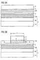
- a carrier material 1 which comprises, for example, a silicon semiconductor material.
- a carrier material 1 comprises, for example, a silicon semiconductor material.
- any other crystalline and approximately lattice-matched support material eg, sapphire, etc. may be used.
- the carrier material 1 can be made, for example, from a semiconductor substrate 1A having a (100) surface orientation, preferably using an Si substrate.
- a semiconductor buffer layer 1B may be epitaxially deposited, wherein preferably a silicon buffer layer is deposited by means of a molecular beam epitaxy (MBE) or MOCVD (Metal Organic Chemical Vapor Deposition) method.
- MBE molecular beam epitaxy
- MOCVD Metal Organic Chemical Vapor Deposition
- a crystalline stress generator layer SG is formed on the substrate 1 or the smoothed output surface of the semiconductor buffer layer 1B, wherein the crystal structure of this stress generator layer SG has substantially a first lattice constant for generating a mechanical stress in the later formed stress-absorbing semiconductor layer.
- the stress generator layer SG has, for example, an IV-IV or a III-V semiconductor. However, it may also have a multi-layer sequence and / or gradually change by means of a molecular beam epitaxy process, again providing improved growth properties for the subsequent layers.
- this stress generator layer SG having a typical thickness of 10 to 300 nanometers is preferably formed by a MOCVD (Metal Organic Chemical Vapor Deposition) method.
- MOCVD Metal Organic Chemical Vapor Deposition
- Each successively formed crystal layer having a significantly smaller thickness will consequently align its lattice constant relative to this uppermost layer.
- the method according to the invention now involves the formation of a stress transmission layer 2 transmitting the generated mechanical stress, which also has insulating properties.
- thermally formed or deposited insulator layers such as oxide layers have an amorphous structure, they are basically not suitable as stress-transmitting layers.
- crystalline insulator layers having a predetermined crystal structure can pass such mechanical stresses generated in the stress generator layer SG to a subsequent stress-receiving semiconductor layer SA.
- crystalline insulator layers for example, CdF 2 , CaF 2 and the like are known.
- CaF is preferably 2 -Stressübertragungs Mrs 2 as buried insulator deposited by means of, for example, an atomic layer deposition method (ALCVD, Atomic Layer Chemical Vapor Deposition) or an MBE method.
- ACVD Atomic Layer Chemical Vapor Deposition
- MBE MBE method
- the actual stress-absorbing semiconductor layer SA is formed on the surface of the stress-transmitting insulating layer 2, preferably forming a silicon semiconductor layer as an active region, e.g. Channel region K, is formed for the semiconductor device.
- a silicon semiconductor layer as an active region, e.g. Channel region K
- the insulating stress transfer layer 2 ensures the reliable and complete depletion of this stressed or stress-absorbing semiconductor layer SA, which is why, in addition to the improved charge carrier mobility, all the advantages of a completely depleted semiconductor component are also achieved receives. Furthermore, since the stress transfer layer 2 has only a few atomic layers and is optimally adapted in terms of lattice constants in the case of CaF 2 and Si, the mechanical stress generated in the stress generator layer SG is passed on to the stress-receiving semiconductor layer SA virtually without loss.
- a gate dielectric 3 and a control layer 4 are formed on the surface of the stress-receiving semiconductor layer SA.
- the gate dielectric 3 may for example consist of conventional gate dielectrics such as silicon nitride, silicon dioxide, ONO layer sequences or future new high-k dielectrics, etc.
- the control layer 4 likewise consist of conventional gate materials such as doped polysilicon or metal can.
- high dielectric constant gate dielectrics or so-called high-k dielectrics are used as the gate dielectric, wherein preferably HfO 2 , HfSi x O y , HfSiNO, etc., again by means of an ALCVD or MOCVD method in a thickness of typical 3 nanometers is deposited. Due to the dramatic mismatching of the lattice constants of these materials, ie, the gate dielectric, and the low deposition temperatures to the stress-receiving semiconductor layer SA, the deposition process is amorphous.
- a so-called mid-gap material is deposited as the gate material, in particular in the case of the intended complete depletion of the active semiconductor body. Such materials may favorably influence interactions with the high-k materials of the gate dielectric 3, wherein in the case of the hafnium gate materials mentioned above, a metal gate such as TiN is preferably used as the control layer 4.
- both the control layer 4 and the gate dielectric 3 are structured and formed in the stress-absorbing semiconductor layer SA respective source and drain regions S and D for completing a field effect transistor.
- the further steps for the formation of spacers, contact holes, connection areas, etc. correspond to the prior art, which is why a description is omitted below.
- semiconductor devices with stressed or stress-absorbing and / or completely depletion semiconductor layers can be produced in a simple and cost-effective manner, whereby in particular a turn-off (off-current) is reduced and a charge carrier mobility and thus clock rate of the semiconductor device is improved ,
- the equivalent oxide thicknesses (EOT, Equivalent Oxide Thickness) can be reduced, whereby the control can be improved and in particular reduced voltages can be realized.
- the insulating stress transfer layer also reduces punch-through effects and, in particular, can significantly reduce off-state leakage current.
- a corresponding layer structure is now also available for sub-100 nanometer semiconductor devices with which semiconductor devices with small deviations of the electrical properties and sufficient reproducibility can be manufactured.
- the invention has been described above with reference to an nMOSFET. However, it is not limited thereto and likewise includes pMOSFETs or other semiconductor devices with stress-absorbing semiconductor layer. Furthermore, the invention has been based on a stress-absorbing silicon Semiconductor layer and a CaF 2 existing stress transfer layer described. However, alternative materials for realizing these layers can be used in the same way.
Landscapes
- Thin Film Transistor (AREA)
- Insulated Gate Type Field-Effect Transistor (AREA)
- Recrystallisation Techniques (AREA)
Abstract
Claims (20)
- Composant à semiconducteur ayant une couche semiconductrice bloquée, comprenant :un matériau (1) de support ayant une première constante de réseau ;une première couche (SG) cristalline, qui est formée sur le matériau (1) de support et qui a, dans sa dernière couche d'atome, une deuxième constante de réseau différente de la première constante de réseau pour la production d'une contrainte mécanique ;une deuxième couche (2) isolante, qui est formée sur la première couche (SG) et qui a une troisième constante de réseau adaptée au matériau (1) de support pour la transmission de la contrainte mécanique produite ;un couche (SA) semiconductrice cristalline bloquée formée sur la deuxième couche (2) et ayant une constante de réseau différente de la deuxième constante de réseau pour l'absorption de la contrainte mécanique transmise et pour la réalisation de zones (S, D) de source/drain ainsi que d'une zone (K) de canal ;un diélectrique (3) de grille formé au moins à la surface de la zone (K) de canal ; etune couche (4) de commande formée sur le diélectrique (3) de grille pour la commande de la zone (K) de canal.
- Composant à semiconducteur suivant la revendication 1, caractérisé en ce que la couche (SA) semiconductrice bloquée a une épaisseur (d) plus petite que le tiers d'une longueur (L) de la zone (K) de canal.
- Composant à semiconducteur suivant la revendication 1 ou 2, caractérisé en ce que la deuxième couche (2) constitue une couche cristalline isolante.
- Composant à semiconducteur suivant la revendication 3, caractérisé en ce que la deuxième couche (2) a une constante de réseau adaptée à la constante de réseau de la couche (SA) semiconductrice bloquée.
- Composant à semiconducteur suivant l'une des revendications 1 à 4,
caractérisé en ce que la première couche (SG) est une couche en SiGe d'une épaisseur de 10 à 300 nm,
la deuxième couche (2) une couche en CaF2 d'une épaisseur de 1 à 2 nm et
la couche (SA) semiconductrice bloquée une couche en Si d'une épaisseur de 5 nm. - Composant à semiconducteur suivant l'une des revendications 1 à 5,
caractérisé en ce que le diélectrique (3) de grille a une grande constante diélectrique. - Composant à semiconducteur suivant l'une des revendications 1 à 6,
caractérisé en ce que la couche (4) de commande comporte un métal. - Composant à semiconducteur suivant l'une des revendications 1 à 7,
caractérisé en ce que le matériau (1) de support comprend un substrat (1A) en Si ayant une orientation de surface (100) et
une couche (1B) tampon en Si pour la production d'une surface de sortie lisse pour la première couche (SG). - Procédé de production d'un composant à semiconducteur ayant une couche semiconductrice bloquée, comprenant les stades, dans desquels :a) on forme un matériau (1) de support ayant une première constante de réseau ;b) on forme une première couche (SG) cristalline, qui a, dans sa dernière couche d'atome, une deuxième constante de réseau différente de la première constante de réseau sur le matériau (1) de support pour la production d'une contrainte mécanique ;c) on forme une deuxième couche (2) isolante sur la première couche (SG) pour la transmission de la contrainte mécanique produite, qui a une troisième constante de réseau adaptée au matériau (1) de support ;d) on forme une couche (SA) semiconductrice cristalline bloquée ayant une constante de réseau différente de la deuxième constante de réseau sur la deuxième couche (2) pour l'absorption de la contrainte mécanique ;e) on forme un diélectrique (3) de grille sur la couche (SA) semiconductrice bloquée ;f) on forme une couche (4) de commande sur le diélectrique (3) de grille ;g) on structure le diélectrique (3) de grille et la couche (4) de commande ; eth) on forme des zones (S, D) de source/drain dans la couche (SA) semiconductrice bloquée.
- Procédé suivant la revendication 9,
caractérisé en ce que
au stade a), on se procure un substrat (1A) semiconducteur ayant une orientation de surface (100) et, pour la production d'une surface lisse, on y dépose par épitaxie une couche (1B) tampon semiconductrice. - Procédé suivant la revendication 9 ou 10,
caractérisé en ce que
au stade b), on utilise un semiconducteur IV-IV ou III-V. - Procédé suivant la revendication 11,
caractérisé en ce que
au stade d), on forme comme première couche (SG) une succession de couches multiples. - Procédé suivant l'une des revendications 9 à 12,
caractérisé en ce que
au stade b), on rend lisse la première couche (SG) au moyen d'un procédé d'épitaxie par faisceau moléculaire. - Procédé suivant l'une des revendications 9 à 13,
caractérisé en ce que
au stade c), on forme la couche cristalline isolante en tant que deuxième couche (2). - Procédé suivant la revendication 14,
caractérisé en ce que
au stade c), on forme la deuxième couche (2) avec une constante de réseau adaptée à la constante de réseau de la couche (SA) semiconductrice bloquée. - Procédé suivant la revendication 15,
caractérisé en ce que
au stade c), on ne dépose par épitaxie que quelques couches d'atome de la deuxième couche (2) sur la première couche (SG). - Procédé suivant l'une des revendications 9 à 16,
caractérisé en ce que
au stade d), on utilise un matériau semiconducteur appauvri complètement. - Procédé suivant l'une des revendications 9 à 17,
caractérisé en ce que
au stade e), on utilise comme diélectrique (3) de grille un matériau ayant une grande constante diélectrique. - Procédé suivant l'une des revendications 9 à 18,
caractérisé en ce que
au stade f), on utilise un métal comme couche (4) de commande. - Procédé suivant l'une des revendications 9 à 19,
caractérisé en ce qu'on utilise
au stade a), Si comme matériau (1) de support ;
au stade b), SiGe comme première couche (SG) ;
au stade c), CaF2 comme deuxième couche (2) ;
au stade d), Si comme couche (SA) semiconductrice bloquée ;
au stade e), HfO2 comme diélectrique (3) de grille ; et
au stade f), TiN comme couche (4) de commande.
Applications Claiming Priority (3)
| Application Number | Priority Date | Filing Date | Title |
|---|---|---|---|
| DE10231964 | 2002-07-15 | ||
| DE10231964A DE10231964A1 (de) | 2002-07-15 | 2002-07-15 | Halbleiterbauelement mit stressaufnehmender Halbleiterschicht sowie zugehöriges Herstellungsverfahren |
| PCT/DE2003/002352 WO2004010485A2 (fr) | 2002-07-15 | 2003-07-11 | Composant a semiconducteur pourvu d'une couche semiconductrice absorbant les contraintes et procede de fabrication correspondant |
Publications (2)
| Publication Number | Publication Date |
|---|---|
| EP1522092A2 EP1522092A2 (fr) | 2005-04-13 |
| EP1522092B1 true EP1522092B1 (fr) | 2011-08-31 |
Family
ID=30468983
Family Applications (1)
| Application Number | Title | Priority Date | Filing Date |
|---|---|---|---|
| EP03764890A Expired - Lifetime EP1522092B1 (fr) | 2002-07-15 | 2003-07-11 | Composant a semiconducteur pourvu d'une couche semiconductrice absorbant les contraintes et procede de fabrication correspondant |
Country Status (6)
| Country | Link |
|---|---|
| US (2) | US7642544B2 (fr) |
| EP (1) | EP1522092B1 (fr) |
| CN (1) | CN100380589C (fr) |
| DE (1) | DE10231964A1 (fr) |
| TW (1) | TWI234285B (fr) |
| WO (1) | WO2004010485A2 (fr) |
Families Citing this family (9)
| Publication number | Priority date | Publication date | Assignee | Title |
|---|---|---|---|---|
| US6707106B1 (en) * | 2002-10-18 | 2004-03-16 | Advanced Micro Devices, Inc. | Semiconductor device with tensile strain silicon introduced by compressive material in a buried oxide layer |
| US7612366B2 (en) | 2003-06-26 | 2009-11-03 | Mears Technologies, Inc. | Semiconductor device including a strained superlattice layer above a stress layer |
| US7586158B2 (en) | 2005-07-07 | 2009-09-08 | Infineon Technologies Ag | Piezoelectric stress liner for bulk and SOI |
| WO2007011627A1 (fr) * | 2005-07-15 | 2007-01-25 | Mears Technologies, Inc. | Dispositif à semi-conducteur comprenant une couche à hétérostructure contrainte sur une couche de contrainte et procédés associés |
| US8389300B2 (en) * | 2010-04-02 | 2013-03-05 | Centre National De La Recherche Scientifique | Controlling ferroelectricity in dielectric films by process induced uniaxial strain |
| US9793243B2 (en) | 2014-08-13 | 2017-10-17 | Taiwan Semiconductor Manufacturing Company, Ltd. | Buffer layer(s) on a stacked structure having a via |
| US9768254B2 (en) | 2015-07-30 | 2017-09-19 | International Business Machines Corporation | Leakage-free implantation-free ETSOI transistors |
| FR3064398B1 (fr) * | 2017-03-21 | 2019-06-07 | Soitec | Structure de type semi-conducteur sur isolant, notamment pour un capteur d'image de type face avant, et procede de fabrication d'une telle structure |
| CN108821231B (zh) * | 2018-06-26 | 2019-08-09 | 清华大学 | 一种基于力学原理的表面具有微结构的高弹性基体及方法 |
Family Cites Families (8)
| Publication number | Priority date | Publication date | Assignee | Title |
|---|---|---|---|---|
| US5232862A (en) * | 1990-07-16 | 1993-08-03 | General Motors Corporation | Method of fabricating a transistor having a cubic boron nitride layer |
| CA2062134C (fr) * | 1991-05-31 | 1997-03-25 | Ibm | Couches hétéroépitaxiales à faible densité de défauts et parmètre de réseau arbitraire |
| US5453399A (en) * | 1993-10-06 | 1995-09-26 | Texas Instruments Incorporated | Method of making semiconductor-on-insulator structure |
| JPH11233440A (ja) | 1998-02-13 | 1999-08-27 | Toshiba Corp | 半導体装置 |
| CA2345122A1 (fr) | 1998-09-25 | 2000-04-06 | Asahi Kasei Kabushiki Kaisha | Substrat a semi-conducteur et son procede de fabrication, dispositif a semi-conducteur comprenant un tel substrat et son procede de fabrication |
| KR100429869B1 (ko) * | 2000-01-07 | 2004-05-03 | 삼성전자주식회사 | 매몰 실리콘 저머늄층을 갖는 cmos 집적회로 소자 및기판과 그의 제조방법 |
| KR100385857B1 (ko) * | 2000-12-27 | 2003-06-02 | 한국전자통신연구원 | SiGe MODFET 소자 제조방법 |
| US6475857B1 (en) * | 2001-06-21 | 2002-11-05 | Samsung Electronics Co., Ltd. | Method of making a scalable two transistor memory device |
-
2002
- 2002-07-15 DE DE10231964A patent/DE10231964A1/de not_active Ceased
-
2003
- 2003-07-11 US US10/521,498 patent/US7642544B2/en not_active Expired - Fee Related
- 2003-07-11 WO PCT/DE2003/002352 patent/WO2004010485A2/fr not_active Ceased
- 2003-07-11 TW TW092119074A patent/TWI234285B/zh not_active IP Right Cessation
- 2003-07-11 EP EP03764890A patent/EP1522092B1/fr not_active Expired - Lifetime
- 2003-07-11 CN CNB038167840A patent/CN100380589C/zh not_active Expired - Fee Related
-
2009
- 2009-10-27 US US12/606,876 patent/US8198681B2/en not_active Expired - Fee Related
Non-Patent Citations (1)
| Title |
|---|
| TEZUKA T ET AL: "Novel fully-depleted SiGe-on-insulator pMOSFETs with high-mobility SiGe surface channels", INTERNATIONAL ELECTRON DEVICES MEETING 2001. IEDM. TECHNICAL DIGEST. WASHINGTON, DC, DEC. 2 - 5, 2001; [INTERNATIONAL ELECTRON DEVICES MEETING], NEW YORK, NY : IEEE, US, 2 December 2001 (2001-12-02), pages 33.6_1 - 33.6_3, XP010575278, ISBN: 978-0-7803-7050-0 * |
Also Published As
| Publication number | Publication date |
|---|---|
| US8198681B2 (en) | 2012-06-12 |
| WO2004010485A3 (fr) | 2004-05-06 |
| TW200403775A (en) | 2004-03-01 |
| US20100084691A1 (en) | 2010-04-08 |
| EP1522092A2 (fr) | 2005-04-13 |
| US7642544B2 (en) | 2010-01-05 |
| US20060118867A1 (en) | 2006-06-08 |
| WO2004010485A2 (fr) | 2004-01-29 |
| CN1669123A (zh) | 2005-09-14 |
| CN100380589C (zh) | 2008-04-09 |
| DE10231964A1 (de) | 2004-02-19 |
| TWI234285B (en) | 2005-06-11 |
Similar Documents
| Publication | Publication Date | Title |
|---|---|---|
| DE112008000571B4 (de) | Nicht-planarer Transistor mit einem Quantentopfkanal und Verfahren zu dessen Herstellung | |
| DE112011106092B3 (de) | Halbleiter, der durch elastische Kantenrelaxation eines Stressors in Kombination mit einer vergrabenen Isolierschicht verspannt wird | |
| EP1604390B1 (fr) | Procede de production d'une structure lamellaire liberant la contrainte sur un substrat non adapte en grille et utilisation d'un tel systeme lamellaire dans des composants electroniques et/ou optoelectroniques | |
| DE112012000689B4 (de) | Halbleiterstruktur mit Gate-Dielektrikum aus Nitrid und Verfahren zum Bilden der Halbleiterstruktur | |
| DE69838307T2 (de) | Vertikal-Sperrschicht-Feldeffekttransistoren | |
| DE112012004932B4 (de) | Verfahren zur Herstellung eines SOI-FinFET mit vertieften verschmolzenen Rippen und Schicht zur verbesserten Spannungskopplung | |
| DE69121535T2 (de) | Feldeffekttransistor mit inverser T-förmiger Silizid-Torelektrode | |
| EP1697998B1 (fr) | Transistor a effet de champ dote d'une structure a couches heterogenes et procede de fabrication associe | |
| DE10296953B4 (de) | Herstellungsverfahren für einen Doppelgatetransistor | |
| DE112006003439B4 (de) | Verfahren zur Herstellung eines n-Kanal-Transistors und n-Kanal-Transistor | |
| DE102009010883B4 (de) | Einstellen eines nicht-Siliziumanteils in einer Halbleiterlegierung während der FET-Transistorherstellung mittels eines Zwischenoxidationsprozesses | |
| DE112010002895T5 (de) | Verfahren und Struktur zur Bildung leistungsstarker FETs mit eingebetteten Stressoren | |
| DE102012111822B4 (de) | Vorrichtung und Verfahren für Multi-Gate-Transistoren | |
| DE102007009914A1 (de) | Feldeffekttransistor mit einem Zwischenschichtdielektrikumsmaterial mit erhöhter innerer Verspannung | |
| DE602004011776T2 (de) | Halbleiterbauelement, verfahren zur herstellung einer quantentopfstruktur und halbleiterbauelement eine solche quantentopfstruktur beinhaltend | |
| DE112004002307T5 (de) | Transistor mit Silizium- und Kohlenstoffschicht in dem Kanalbereich | |
| DE112004002373T5 (de) | Strained-Transistor-Integration für CMOS | |
| DE102014210406B4 (de) | Verfahren zur Herstellung eines Transistors mit einem verspannten Kanalgebiet | |
| DE10318283A1 (de) | Verfahren zur Herstellung einer verspannten Schicht auf einem Substrat und Schichtstruktur | |
| US8198681B2 (en) | Semiconductor component with stress-absorbing semiconductor layer | |
| DE10229003B4 (de) | Ein Verfahren zur Herstellung eines SOI-Feldeffekttransistorelements mit einem Rekombinationsgebiet | |
| DE102008044983B4 (de) | Verfahren zum Herstellen eines strukturierten verformten Substrats, insbesondere zur Herstellung verformter Transistoren mit geringerer Dicke der aktiven Schicht | |
| EP1497855B1 (fr) | Procede de production d'une ou plusieurs couches monocristallines dotee chacune d'une structure reticulaire differente dans un plan d'une suite de couches | |
| DE102004033147B4 (de) | Planarer Doppel-Gate-Transistor und Verfahren zum Herstellen eines planaren Doppel-Gate-Transistors | |
| DE102019117775B4 (de) | Halbleiterstruktur und verfahren zu deren herstellung |
Legal Events
| Date | Code | Title | Description |
|---|---|---|---|
| PUAI | Public reference made under article 153(3) epc to a published international application that has entered the european phase |
Free format text: ORIGINAL CODE: 0009012 |
|
| 17P | Request for examination filed |
Effective date: 20041223 |
|
| AK | Designated contracting states |
Kind code of ref document: A2 Designated state(s): AT BE BG CH CY CZ DE DK EE ES FI FR GB GR HU IE IT LI LU MC NL PT RO SE SI SK TR |
|
| RBV | Designated contracting states (corrected) |
Designated state(s): DE FR IT |
|
| 17Q | First examination report despatched |
Effective date: 20080114 |
|
| RAP1 | Party data changed (applicant data changed or rights of an application transferred) |
Owner name: INFINEON TECHNOLOGIES AG |
|
| GRAP | Despatch of communication of intention to grant a patent |
Free format text: ORIGINAL CODE: EPIDOSNIGR1 |
|
| RIC1 | Information provided on ipc code assigned before grant |
Ipc: H01L 29/786 20060101ALI20110208BHEP Ipc: H01L 29/10 20060101ALI20110208BHEP Ipc: H01L 21/762 20060101ALI20110208BHEP Ipc: H01L 21/20 20060101AFI20110208BHEP Ipc: H01L 21/02 20060101ALI20110208BHEP Ipc: H01L 21/314 20060101ALI20110208BHEP |
|
| GRAS | Grant fee paid |
Free format text: ORIGINAL CODE: EPIDOSNIGR3 |
|
| GRAA | (expected) grant |
Free format text: ORIGINAL CODE: 0009210 |
|
| AK | Designated contracting states |
Kind code of ref document: B1 Designated state(s): DE FR IT |
|
| REG | Reference to a national code |
Ref country code: DE Ref legal event code: R096 Ref document number: 50313938 Country of ref document: DE Effective date: 20111027 |
|
| PLBE | No opposition filed within time limit |
Free format text: ORIGINAL CODE: 0009261 |
|
| STAA | Information on the status of an ep patent application or granted ep patent |
Free format text: STATUS: NO OPPOSITION FILED WITHIN TIME LIMIT |
|
| 26N | No opposition filed |
Effective date: 20120601 |
|
| REG | Reference to a national code |
Ref country code: DE Ref legal event code: R097 Ref document number: 50313938 Country of ref document: DE Effective date: 20120601 |
|
| REG | Reference to a national code |
Ref country code: FR Ref legal event code: PLFP Year of fee payment: 14 |
|
| REG | Reference to a national code |
Ref country code: FR Ref legal event code: PLFP Year of fee payment: 15 |
|
| PGFP | Annual fee paid to national office [announced via postgrant information from national office to epo] |
Ref country code: IT Payment date: 20170728 Year of fee payment: 15 Ref country code: DE Payment date: 20170912 Year of fee payment: 15 Ref country code: FR Payment date: 20170724 Year of fee payment: 15 |
|
| REG | Reference to a national code |
Ref country code: DE Ref legal event code: R119 Ref document number: 50313938 Country of ref document: DE |
|
| PG25 | Lapsed in a contracting state [announced via postgrant information from national office to epo] |
Ref country code: DE Free format text: LAPSE BECAUSE OF NON-PAYMENT OF DUE FEES Effective date: 20190201 Ref country code: FR Free format text: LAPSE BECAUSE OF NON-PAYMENT OF DUE FEES Effective date: 20180731 |
|
| PG25 | Lapsed in a contracting state [announced via postgrant information from national office to epo] |
Ref country code: IT Free format text: LAPSE BECAUSE OF NON-PAYMENT OF DUE FEES Effective date: 20180711 |