EP1521297A1 - Plasmaverarbeitungsgerät - Google Patents
Plasmaverarbeitungsgerät Download PDFInfo
- Publication number
- EP1521297A1 EP1521297A1 EP03741183A EP03741183A EP1521297A1 EP 1521297 A1 EP1521297 A1 EP 1521297A1 EP 03741183 A EP03741183 A EP 03741183A EP 03741183 A EP03741183 A EP 03741183A EP 1521297 A1 EP1521297 A1 EP 1521297A1
- Authority
- EP
- European Patent Office
- Prior art keywords
- plasma
- processing apparatus
- microwave
- plasma gas
- gas
- Prior art date
- Legal status (The legal status is an assumption and is not a legal conclusion. Google has not performed a legal analysis and makes no representation as to the accuracy of the status listed.)
- Granted
Links
Images


Classifications
-
- C—CHEMISTRY; METALLURGY
- C23—COATING METALLIC MATERIAL; COATING MATERIAL WITH METALLIC MATERIAL; CHEMICAL SURFACE TREATMENT; DIFFUSION TREATMENT OF METALLIC MATERIAL; COATING BY VACUUM EVAPORATION, BY SPUTTERING, BY ION IMPLANTATION OR BY CHEMICAL VAPOUR DEPOSITION, IN GENERAL; INHIBITING CORROSION OF METALLIC MATERIAL OR INCRUSTATION IN GENERAL
- C23C—COATING METALLIC MATERIAL; COATING MATERIAL WITH METALLIC MATERIAL; SURFACE TREATMENT OF METALLIC MATERIAL BY DIFFUSION INTO THE SURFACE, BY CHEMICAL CONVERSION OR SUBSTITUTION; COATING BY VACUUM EVAPORATION, BY SPUTTERING, BY ION IMPLANTATION OR BY CHEMICAL VAPOUR DEPOSITION, IN GENERAL
- C23C16/00—Chemical coating by decomposition of gaseous compounds, without leaving reaction products of surface material in the coating, i.e. chemical vapour deposition [CVD] processes
- C23C16/44—Chemical coating by decomposition of gaseous compounds, without leaving reaction products of surface material in the coating, i.e. chemical vapour deposition [CVD] processes characterised by the method of coating
- C23C16/455—Chemical coating by decomposition of gaseous compounds, without leaving reaction products of surface material in the coating, i.e. chemical vapour deposition [CVD] processes characterised by the method of coating characterised by the method used for introducing gases into reaction chamber or for modifying gas flows in reaction chamber
- C23C16/45563—Gas nozzles
- C23C16/45568—Porous nozzles
-
- H—ELECTRICITY
- H10—SEMICONDUCTOR DEVICES; ELECTRIC SOLID-STATE DEVICES NOT OTHERWISE PROVIDED FOR
- H10P—GENERIC PROCESSES OR APPARATUS FOR THE MANUFACTURE OR TREATMENT OF DEVICES COVERED BY CLASS H10
- H10P50/00—Etching of wafers, substrates or parts of devices
- H10P50/20—Dry etching; Plasma etching; Reactive-ion etching
- H10P50/24—Dry etching; Plasma etching; Reactive-ion etching of semiconductor materials
- H10P50/242—Dry etching; Plasma etching; Reactive-ion etching of semiconductor materials of Group IV materials
-
- C—CHEMISTRY; METALLURGY
- C23—COATING METALLIC MATERIAL; COATING MATERIAL WITH METALLIC MATERIAL; CHEMICAL SURFACE TREATMENT; DIFFUSION TREATMENT OF METALLIC MATERIAL; COATING BY VACUUM EVAPORATION, BY SPUTTERING, BY ION IMPLANTATION OR BY CHEMICAL VAPOUR DEPOSITION, IN GENERAL; INHIBITING CORROSION OF METALLIC MATERIAL OR INCRUSTATION IN GENERAL
- C23C—COATING METALLIC MATERIAL; COATING MATERIAL WITH METALLIC MATERIAL; SURFACE TREATMENT OF METALLIC MATERIAL BY DIFFUSION INTO THE SURFACE, BY CHEMICAL CONVERSION OR SUBSTITUTION; COATING BY VACUUM EVAPORATION, BY SPUTTERING, BY ION IMPLANTATION OR BY CHEMICAL VAPOUR DEPOSITION, IN GENERAL
- C23C16/00—Chemical coating by decomposition of gaseous compounds, without leaving reaction products of surface material in the coating, i.e. chemical vapour deposition [CVD] processes
- C23C16/44—Chemical coating by decomposition of gaseous compounds, without leaving reaction products of surface material in the coating, i.e. chemical vapour deposition [CVD] processes characterised by the method of coating
- C23C16/50—Chemical coating by decomposition of gaseous compounds, without leaving reaction products of surface material in the coating, i.e. chemical vapour deposition [CVD] processes characterised by the method of coating using electric discharges
- C23C16/511—Chemical coating by decomposition of gaseous compounds, without leaving reaction products of surface material in the coating, i.e. chemical vapour deposition [CVD] processes characterised by the method of coating using electric discharges using microwave discharges
-
- H—ELECTRICITY
- H01—ELECTRIC ELEMENTS
- H01J—ELECTRIC DISCHARGE TUBES OR DISCHARGE LAMPS
- H01J37/00—Discharge tubes with provision for introducing objects or material to be exposed to the discharge, e.g. for the purpose of examination or processing thereof
- H01J37/32—Gas-filled discharge tubes
- H01J37/32009—Arrangements for generation of plasma specially adapted for examination or treatment of objects, e.g. plasma sources
- H01J37/32192—Microwave generated discharge
- H01J37/32211—Means for coupling power to the plasma
- H01J37/32238—Windows
-
- H—ELECTRICITY
- H01—ELECTRIC ELEMENTS
- H01J—ELECTRIC DISCHARGE TUBES OR DISCHARGE LAMPS
- H01J37/00—Discharge tubes with provision for introducing objects or material to be exposed to the discharge, e.g. for the purpose of examination or processing thereof
- H01J37/32—Gas-filled discharge tubes
- H01J37/32431—Constructional details of the reactor
- H01J37/3244—Gas supply means
Definitions
- the present invention generally relates to plasma processing apparatuses and more particularly to a microwave plasma processing apparatus.
- Plasma processing and plasma processing apparatus are indispensable technology for the fabrication of ultrafine semiconductor devices of recent years called deep submicron devices or deep sub-quarter micron devices having a gate length near 0.1 ⁇ m or less or for the fabrication of high-resolution flat panel display devices including a liquid crystal display device.
- a microwave plasma processing apparatus that uses high-density plasma excited by a microwave electric field without using a d.c. magnetic field.
- a plasma processing apparatus having a construction in which a microwave is emitted into a processing vessel from a planar antenna (radial-line slot antenna) having a number of slots arranged to produce a uniform microwave.
- plasma processing apparatus plasma is excited as a result of the microwave electric field causing ionization in the gas inside the evacuated vessel.
- Japanese Laid-Open Patent Application 9-63793 Japanese Laid-Open Patent Application 9-63793.
- the microwave plasma excited according to such a process it becomes possible to realize a high plasma density over a wide area underneath the antenna, and it becomes possible to conduct uniform plasma processing in short time. Further, because the electron density is low in the microwave plasma thus excited due to the use of microwave for the excitation of the plasma, it becomes possible to avoid damaging or metal contamination of the substrate to be processed. Further, because it is possible to excite uniform plasma over a large area substrate, the foregoing technology can easily attend to the fabrication of semiconductor devices that uses a large-diameter semiconductor substrate or production of large liquid crystal display devices.
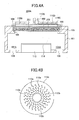
- Figures 1A and 1B show the construction of a conventional microwave plasma processing apparatus 100 that uses such a radial line slot antenna, wherein Figure 1A is a cross-sectional view of the microwave plasma processing apparatus 100, while Figure 1B shows the construction of the radial line slot antenna.
- the microwave plasma processing apparatus 100 has a processing chamber 101 evacuated from plural evacuation ports 116, and a stage 115 that holds a substrate 114 to be processed is formed inside the processing chamber 101.
- a ring-shaped space 101A around the stage 115 wherein the processing chamber 101 can be evacuated uniformly via the space 101A and the evacuation ports 116 by forming the plural evacuation ports 116 in communication with the space 101A with equal interval, in other words, in axial symmetry with regard to the substrate to be processed.
- a shower plate 103 of low-loss dielectric material with a plate-like form wherein the shower plate 103 has a number of apertures 107 and is provided via a seal ring 109 as a part of the outer wall of the processing vessel 101 at a location corresponding to the substrate 114 to be processed on the stage 115.
- a cover plate 102 also of a low loss dielectric material is provided outside the shower plate 103 via another seal ring 108.
- a passage 104 of a plasma gas On the shower plate 103, there is formed a passage 104 of a plasma gas on the top surface thereof, and each of the plural apertures 107 is formed in communication with the plasma gas passage 104. Further, there is formed a supply passage 108 of the plasma gas inside the shower plate 103 in communication with a plasma gas supplying port 105 provided on the outer wall of the processing vessel 101. Thereby, a plasma gas such as Ar or Kr is supplied to the plasma gas supplying port 105, wherein the plasma gas thus supplied is further supplied to the apertures 107 from the supply passage 108 via the passage 104. The plasma gas is then released into a space 101B right underneath the shower plate 103 inside the processing vessel 101 from the apertures 107 with substantially uniform concentration.
- a radial line slot antenna 110 having a radiation surface shown in Figure 1B at the outer side of the cover plate 102 with a separation of 4 - 5mm from the cover plate 102.
- the radial line slot antenna 110 is connected to an external microwave source (not shown) via a coaxial waveguide 110A, and the microwave from the microwave source causes excitation of the plasma gas released into the foregoing succession 101B. Further, the gap between the cover plate 102 and the radiation surface of the radial line slot antenna 110 is filled with the air.
- the radial line slot antenna 110 is formed of a flat, disk-like antenna body 110B connected to an external waveguide forming the coaxial waveguide 110A, and a radiation plate 110C is formed at the mouth of the antenna body 110B, wherein the radiation plate 110C is formed with a number of slots 110a and a number of slots 110b perpendicular to the slots 110a. Further, there is interposed a retardation plate 110D of a dielectric plate having a uniform thickness between the antenna body 110B and the radiation plate 110C.
- the microwave supplied from the coaxial waveguide 110 spreads as it travels between the disk-like antenna body 110B and the radiation plate 110C in the radial direction, wherein the retardation plate 110D functions to compress the wavelength thereof.
- the retardation plate 110D functions to compress the wavelength thereof.
- the high-density plasma thus formed has the feature of low electron temperature, and thus, there is caused no damaging in the substrate 114 to be processed. Further, there is caused no metal contamination originating from the sputtering of the chamber wall of the processing vessel 101.
- a conductive structure 111 inside the processing vessel 101 between the shower plate 103 and the substrate 114 to be processed, wherein the conductive structure 111 is formed with a large number of nozzles 113 supplied with a processing gas from an external processing gas source (not shown) via a processing gas passage 112 formed in the processing vessel 101, wherein each of the nozzles 113 releases the supplied processing gas to a space 101C between the conductive structure 111 and the substrate 114 to be processed.
- the conductive structure 111 functions as a processing gas supplying part.
- the conductive structure 111 thus constituting the processing gas supplying part is formed with apertures between adjacent nozzles 113 and 113 with a size allowing efficient passage of the plasma formed in the space 101B into the space 101C as a result of diffusion.
- the processing gas is released into the space 101C from the processing gas supplying part 111 via the nozzles 113, the released processing gas undergoes excitation in the processing space 101B by the high-density plasma and there is conducted a uniform plasma processing on the substrate 114 to be processed, efficiently and at high speed, without damaging the substrate and the device structure on the substrate and without contaminating the substrate.
- the microwave emitted from the radial line slot antenna 110 is blocked by the process gas supplying part 111 formed of a conductor, and thus, there is no risk that the substrate 114 to be processed is damaged.
- the plasma is actually excited in the present apparatus 10
- the plasma is also excited in the plasma gas passage 104 and further in the apertures 107 depending on the condition of the substrate processing.
- the microwave power is consumed and the plasma density in the space 101B is decreased.
- the problem of non-uniformity in the plasma density over the entire space 101B which serves for the plasma excitation space.
- Another and more specific object of the present invention is to excite high-density plasma in a desired space with excellent uniformity, without causing plasma excitation in a space in the path for introducing a plasma gas.
- Another object of the present invention is to provide a plasma processing apparatus, comprising:
- the plasma excitation is prevented by using a plasma gas pressure condition set such that there is caused no plasma excitation.
- a mechanism that supplies the plasma gas via pores of a porous medium is employed.
- FIGS. 2A and 2B show the construction of a microwave plasma processing apparatus 200 according to a first embodiment of the present invention, wherein those parts explained previously are designated by the same reference numerals and the description thereof will be omitted.
- the shower plate 103 of the foregoing microwave plasma processing apparatus 103 is replaced with a disk-like shower plate of a porous medium such as a porous ceramic material formed for example by Al 2 O 3 sintered at an ordinary pressure.
- the shower plate 202 is formed with a passage 202 of the plasma gas on the top surface thereof, wherein the plasma gas of Ar or Kr supplied to the plasma gas supplying port 105 is passed through the plasma gas passage 202 and supplied to the space 101B right underneath the shower plate uniformly through the pores in the porous medium that constitutes the shower plate 202.
- FIG 3 shows the region in which excitation of microwave plasma occurs for the case in which the strength of the microwave electric field and the pressure of Ar used for the plasma excitation gas are changed.
- the frequency of the microwave is set to 2.45G.
- region A is the region in which plasma excitation takes place.
- excitation of the microwave plasma takes place at the microwave electric field strength and the Ar pressure of the region A.
- the space 101B used for the plasma excitation space and the plasma gas passage 202, which serves for the plasma gas feeding path, are isolated form each other by the shower plate 201 formed of the porous medium.
- the plasma gas is supplied from the plasma gas passage 202 to the foregoing space 101B through the pores of the porous medium forming the shower plate 201.
- there exist no sufficiently large space in the pores for causing plasma excitation there occurs no excitation of plasma in such pores. More specifically, even when there is caused acceleration of electrons in the pores by the microwave, the electrons collide with the outer wall of the pores before it is accelerated to the degree for causing plasma excitation.
- the present apparatus 200 there is caused no plasma excitation inside the shower plate 201, which serves for the plasma gas inlet continuous to the space 101B, and it becomes possible to excite high-density plasma uniformly in the space 101B.
- FIGS. 4A and 4B show the construction of a microwave plasma processing apparatus 200A according to a second embodiment of the present invention, wherein those parts explained previously are designated with the same reference numerals and the description thereof will be omitted.
- the lower shower plate 111 is removed in the microwave plasma processing apparatus 200A of the present embodiment. Because the lower shower plate 111 is omitted, the apparatus cannot carry out film formation process or etching process by supplying a processing gas separately to the plasma gas. On the other hand, the apparatus can form an oxide film, nitride film or oxynitride film on the surface of the substrate to be processed, by supplying an oxidation gas or nitridation gas from the shower plate 201 together with a plasma gas.
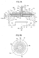
- FIGS. 5A and 5B show the construction of a microwave plasma processing apparatus 10 according to a third embodiment of the present invention.
- the microwave plasma processing apparatus 10 includes a processing vessel 11 and a stage 13 provided in the processing vessel 11, wherein the stage 13 is formed by hot isotropic pressing process of AlN or Al 2 O 3 and holds the substrate 12 to be processed by an electrostatic chuck.
- the processing vessel 11 there are formed at least two, preferably three or more evacuation ports 11a in a space 11A surrounding the stage 13 with a uniform interval, and hence in axial symmetry with regard to the substrate 12 to be processed on the stage 13.
- the processing vessel 11 is evacuated by a vacuum pump via such evacuation ports 11a for reducing the pressure therein.
- the processing vessel 11 is formed of an austenite stainless steel containing Al and a passivation film of aluminum oxide is formed on the inner wall surface thereof by an oxidation processing. Further, there is formed a disk-like shower plate 14 of a porous medium, such as Al 2 O 3 sintered at ordinary temperature in the form of porous ceramic material, in a part of the outer wall of the processing vessel corresponding to the substrate 12 to be processed, wherein the shower plate 14 forms a part of the outer wall.
- a porous medium such as Al 2 O 3 sintered at ordinary temperature in the form of porous ceramic material
- the shower plate 14 is mounted on the processing vessel 11 via a seal ring 11s, wherein there is provided a cover plate 15 of dense Al 2 O 3 formed by HIP processing on the shower plate 14.
- the Al 2 O 3 cover plate 15 thus formed by the HIP process is formed by using Y 2 O 3 as a sintering additive and has the porosity of 0.03% or less. This means that the Al 2 O 3 cover plate 15 is substantially free from pores or pinholes. Further, the Al 2 O 3 cover plate 15 has a very large thermal conductivity for a ceramic, which reaches the value of 30W/mK.
- the shower plate 14 is formed, in the side thereof that makes contact with the cover plate 15, with a depressed plasma gas passage 14A for causing to flow the plasma gas, wherein the foregoing plasma gas passage 14A is connected to a plasma gas inlet 21A formed in the upper part of the shower plate as will be described.
- the shower plate 14 is supported by projections 11b formed on the inner wall of the processing vessel 11, wherein the part of the projection 11b supporting the shower plate 14 is formed to have a rounded surface for suppressing anomalous electric discharge.
- the plasma gas such as Ar or Kr supplied to the plasma gas inlet 21A is supplied to the space 11B right underneath the shower plate uniformly through the pores of the porous medium forming the shower plate 14, after passing through the plasma gas passage 14A inside the shower plate 14. Further, there is inserted a seal ring 15s in the part where the plasma gas inlet 21A and the cover plate 15 engage with each other for confinement of the plasma gas.
- a radial line slot antenna 20 is provided on the cover plate 15, wherein the radial line stop antenna 20 includes a disk-shaped slot plate 16 contacting with the cover plate 15 and formed with numerous slots 16a and 16b shown in Figure 5B, a disk-like antenna body 17 holding the slot plate 16, and a retardation plate 18 of a low-loss dielectric material such as Al 2 O 3 , Si 3 N 4 , SiON, SiO 2 or the like sandwiched between-the slot plate 16 and the antenna body 17. Further, a plasma gas/microwave inlet part 21 is formed on the upper part of the radial line slot antenna 20.
- the foregoing plasma gas/microwave inlet 21 part includes a part 21C connected to the antenna body 17 with circular or rectangular cross-section and forming therein a microwave inlet passage, a microwave inlet part 21B of rectangular or circular cross-section, and a plasma gas inlet passage 21A having a generally cylindrical form.
- a plasma gas such as Ar or Kr is supplied to the plasma gas inlet passage 21A.
- the radial line slot antenna 20 is mounted on the processing vessel 11 via a seal ring 11u, and a microwave of 2.45GHz or 8.3GHz frequency is supplied to the radial line slot antenna from an external microwave source (not shown) connected to the microwave inlet part 21B of the plasma gas/microwave inlet part 21.
- the microwave thus supplied is emitted into the processing vessel 11 through the cover plate 15 and the shower plate 14 after emitted from the slots 16a and 16b on the slot plate 16 and excites plasma in the plasma gas supplied from the shower plate 14 in the space 11B right underneath the shower plate 14.
- the cover plate 15 and the shower plate 14 are formed of Al 2 O 3 and serves for an efficient microwave window.
- the pressure of the plasma gas is maintained to about 6.67kPa - 13.3kPa (about 50 - 100 Torr) in the plasma gas passage 14A for avoiding plasma excitation in the plasma gas passage 14A.
- the foregoing space 11B serving for the plasma excitation space is isolated from the plasma gas passage 14A acting as the passage for supplying the plasma gas, by the shower plate 14 of the porous medium.
- the plasma gas is supplied from the plasma gas passage to the space 11B through the pores in the shower plate 14. Because there is no sufficient space for plasma excitation in the pores, there is caused no plasma excitation.
- such a gap includes not only the slots 16a and 16b formed in the slot plate 16 but also other gaps formed by various reasons. It should be noted that such a gap is sealed by a seal ring 11u provided between the radial line slot antenna 20 and the processing vessel 11.
- the waveguide 21C of the gas/plasma inlet 21 is connected to the disk-shaped antenna body 17, and the plasma gas inlet 21A extends through the opening 18A formed in the retardation plate 18 and the opening 16c formed in the slot plate 16 and is connected to the cover plate opening 15A.
- the microwave supplied to the microwave inlet part 21B is emitted from the slots 16a and 16b as it is propagating in the radial direction between the antenna body 17 and the slot plate 16 after passing through the waveguide 21C.
- Figure 5B shows the slots 16a and 16b formed on the slot plate 16.
- the slots 16a are arranged in a concentric relationship, and in correspondence to each of the slots 16a, there is formed a slot 16b perpendicularly thereto, such that the slots 16b are formed also in a concentric relationship.
- the slots 16a and 16b are formed with an interval corresponding to the wavelength of the microwave compressed by the retardation plate 18 in the radial direction of the slot plate 16, and as a result, the microwave is emitted from the slot plate 16 generally in the form of plane wave. Because the slots 16a and 16b are formed in a mutually perpendicular relationship, the microwave thus emitted form a circular polarization containing two, mutually perpendicular polarization components.
- a cooling block 19 formed with a cooling water passage 19A is formed on the antenna body 17.
- the cooling water passage 19A is formed in a spiral form on the cooling block 19, and cooling water, preferably the one in which oxidation-reduction potential is controlled by eliminating dissolved oxygen by means of bubbling of an H 2 gas, is passed through the cooling water passage 19A.
- a process gas supplying structure 31 having a lattice-shaped process gas passage in the processing vessel 11 between the shower plate 14 and the substrate 12 to be processed on the stage 13, wherein the process gas supplying structure 31 is supplied with a processing gas from a processing gas inlet port 11r provided on the outer wall of the processing vessel and releases the same from a number of processing gas nozzle apertures 31A.
- a desired uniform substrate processing is achieved in the space 11C between the processing gas supplying structure 31 and the substrate 12 to be processed.
- a substrate processing includes plasma oxidation processing, plasma nitridation processing, plasma oxynitridation processing, plasma CVD processing, and the like.
- a fluorocarbon gas such as C 4 F 8 , C 5 F 8 , C 4 F 6 , and the like or an etching gas containing F or Cl from the processing gas supplying structure 31 and further by applying a high-frequency voltage to the stage 13A from a high-frequency source 13A, it becomes possible to conduct a reactive ion etching process on the substrate 12 to be processed.
- microwave plasma processing apparatus 10 of the present embodiment deposition of reaction byproducts on the inner wall surface of the processing vessel is avoided by heating the outer wall of the processing vessel 11 to the temperature of about 150°C, and continuous and stable operation becomes possible by conducting a dry cleaning process once in a day or so.
- FIGS. 6A and 6B show an example of a microwave plasma processing apparatus 10A according to a fourth embodiment of the present invention, wherein those parts explained previously are designated by the same reference numerals and the description thereof will be omitted.
- a plasma gas passage 40A in the form of a depression as the passage of the plasma gas, such that the plasma gas passage 40A communicates each of the apertures 40B.
- each of the apertures 40B is inserted with a plasma gas inlet component 41 of a porous medium such as a porous ceramic of Al 2 O 3 sintered at ordinary pressure.
- the plasma gas of Ar or Kr is supplied to the foregoing space 11B generally uniformly via the pores of the porous medium in the plasma gas inlet component 41, after passing through the plasma gas passage 40A.
- the lower shower plate 31 is removed in the microwave plasma processing apparatus 10b of the present embodiment. Further, the entire surface of the projections 11b supporting the shower plate 14 is provided with a rounded surface.
- the plasma processing apparatus 10B of such a construction cannot achieve film formation or etching by supplying a processing gas separately to the plasma gas because of elimination of the lower shower plate 31, it is possible to form an oxide film, a nitride film or an oxynitride film on the surface of the substrate to be processed by supplying an oxidizing gas or nitriding gas from the shower plate 14 together with the plasma gas.
- FIGS 8A and 8B show an example of a microwave plasma processing apparatus 10C according to a sixth embodiment of the present invention, wherein those parts in the drawings corresponding to the parts explained previously are designated by the same reference numerals and the description thereof will be omitted.
- a plasma gas of Ar or Kr is supplied to the processing vessel 11 with the microwave plasma processing apparatus 10C of the present embodiment by way of the shower plate 40 of dense Al 2 O 3 formed by a HIP process, the shower plate 40 being formed with at least one aperture 40B, and the plasma gas inlet component 41 of a porous medium inserted into the aperture 40B such as a porous ceramic material of sintered Al 2 O 3 , similarly to the case of the microwave plasma processing apparatus 10C explained previously.
- the lower shower plate 31 is eliminated similarly to the case of foregoing apparatus 10B, and the entire surface of the projection 11b holding the shower plate 14 is formed with a rounded surface.
- the plasma processing apparatus 10B of such a construction cannot achieve film formation or etching by supplying a processing gas separately to the plasma gas because of elimination of the lower shower plate 31, it is possible to form an oxide film, a nitride film or an oxynitride film on the surface of the substrate to be processed by supplying an oxidizing gas or nitriding gas from the shower plate 14 together with the plasma gas.
- porous ceramic material of Al 2 O 3 sintered at ordinary pressure As an example of the porous medium, it should be noted that the present invention is not limited to this material.
- the present invention it becomes possible to excite high-density and uniform plasma in a desired plasma excitation space while suppressing plasma excitation in a plasma gas inlet passage, by separating the space for plasma excitation and the plasma gas inlet passage for exciting plasma by a porous medium such as a porous ceramic material in a plasma processing apparatus for processing a substrate.
Landscapes
- Chemical & Material Sciences (AREA)
- Engineering & Computer Science (AREA)
- Physics & Mathematics (AREA)
- Plasma & Fusion (AREA)
- Analytical Chemistry (AREA)
- Chemical Kinetics & Catalysis (AREA)
- General Chemical & Material Sciences (AREA)
- Materials Engineering (AREA)
- Mechanical Engineering (AREA)
- Metallurgy (AREA)
- Organic Chemistry (AREA)
- Plasma Technology (AREA)
- Drying Of Semiconductors (AREA)
- Chemical Vapour Deposition (AREA)
Applications Claiming Priority (3)
| Application Number | Priority Date | Filing Date | Title |
|---|---|---|---|
| JP2002197227A JP4540926B2 (ja) | 2002-07-05 | 2002-07-05 | プラズマ処理装置 |
| JP2002197227 | 2002-07-05 | ||
| PCT/JP2003/008491 WO2004006319A1 (ja) | 2002-07-05 | 2003-07-03 | プラズマ処理装置 |
Publications (3)
| Publication Number | Publication Date |
|---|---|
| EP1521297A1 true EP1521297A1 (de) | 2005-04-06 |
| EP1521297A4 EP1521297A4 (de) | 2006-06-07 |
| EP1521297B1 EP1521297B1 (de) | 2011-02-02 |
Family
ID=30112393
Family Applications (1)
| Application Number | Title | Priority Date | Filing Date |
|---|---|---|---|
| EP03741183A Expired - Lifetime EP1521297B1 (de) | 2002-07-05 | 2003-07-03 | Plasmaverarbeitungsgerät |
Country Status (9)
| Country | Link |
|---|---|
| US (2) | US20050092437A1 (de) |
| EP (1) | EP1521297B1 (de) |
| JP (1) | JP4540926B2 (de) |
| KR (1) | KR100614065B1 (de) |
| CN (1) | CN100405557C (de) |
| AU (1) | AU2003281401A1 (de) |
| DE (1) | DE60335951D1 (de) |
| TW (1) | TWI239052B (de) |
| WO (1) | WO2004006319A1 (de) |
Cited By (3)
| Publication number | Priority date | Publication date | Assignee | Title |
|---|---|---|---|---|
| DE102004039969A1 (de) * | 2004-08-18 | 2006-02-23 | Leybold Optics Gmbh | Plasmaquellenvorrichtung, Anordnung mit einer Plasmaquellenvorrichtung sowie Abstrahleinheit für eine Plasmaquellenvorrichtung |
| US8372200B2 (en) | 2006-06-13 | 2013-02-12 | Tokyo Electron Ltd. | Shower plate, method for manufacturing the shower plate, plasma processing apparatus using the shower plate, plasma processing method and electronic device manufacturing method |
| EP1975986A4 (de) * | 2006-01-20 | 2013-09-11 | Tokyo Electron Ltd | Plasmaverarbeitungsgerät |
Families Citing this family (19)
| Publication number | Priority date | Publication date | Assignee | Title |
|---|---|---|---|---|
| JP4350695B2 (ja) * | 2004-12-01 | 2009-10-21 | 株式会社フューチャービジョン | 処理装置 |
| JP2006244891A (ja) * | 2005-03-04 | 2006-09-14 | Tokyo Electron Ltd | マイクロ波プラズマ処理装置 |
| JP5082229B2 (ja) * | 2005-11-29 | 2012-11-28 | 東京エレクトロン株式会社 | プラズマ処理装置 |
| JP5082459B2 (ja) * | 2006-01-20 | 2012-11-28 | 東京エレクトロン株式会社 | プラズマ処理装置及び天板の製造方法 |
| US20080254220A1 (en) * | 2006-01-20 | 2008-10-16 | Tokyo Electron Limited | Plasma processing apparatus |
| JP4915985B2 (ja) * | 2006-02-06 | 2012-04-11 | 東京エレクトロン株式会社 | プラズマ処理装置およびプラズマ処理方法 |
| US8006640B2 (en) * | 2006-03-27 | 2011-08-30 | Tokyo Electron Limited | Plasma processing apparatus and plasma processing method |
| JP5463536B2 (ja) * | 2006-07-20 | 2014-04-09 | 北陸成型工業株式会社 | シャワープレート及びその製造方法、並びにそのシャワープレートを用いたプラズマ処理装置、プラズマ処理方法及び電子装置の製造方法 |
| JP5004271B2 (ja) * | 2006-09-29 | 2012-08-22 | 東京エレクトロン株式会社 | マイクロ波プラズマ処理装置、誘電体窓の製造方法およびマイクロ波プラズマ処理方法 |
| JP5010234B2 (ja) | 2006-10-23 | 2012-08-29 | 北陸成型工業株式会社 | ガス放出孔部材を一体焼結したシャワープレートおよびその製造方法 |
| JP5058727B2 (ja) * | 2007-09-06 | 2012-10-24 | 東京エレクトロン株式会社 | 天板構造及びこれを用いたプラズマ処理装置 |
| KR101111207B1 (ko) | 2009-05-20 | 2012-02-20 | 주식회사 에이피시스 | 플라즈마 발생장치 |
| JP6101467B2 (ja) * | 2012-10-04 | 2017-03-22 | 東京エレクトロン株式会社 | 成膜方法及び成膜装置 |
| US20150118416A1 (en) * | 2013-10-31 | 2015-04-30 | Semes Co., Ltd. | Substrate treating apparatus and method |
| CN104357810A (zh) * | 2014-11-04 | 2015-02-18 | 大连理工常州研究院有限公司 | 一种同轴微波等离子体沉积薄膜的设备 |
| JP6462449B2 (ja) * | 2015-03-26 | 2019-01-30 | 京セラ株式会社 | 高周波用窓部材および半導体製造装置用部材ならびにフラットパネルディスプレイ(fpd)製造装置用部材 |
| WO2016128560A2 (en) * | 2016-02-12 | 2016-08-18 | Applied Materials, Inc. | Vacuum processing system and methods therefor |
| US11776793B2 (en) * | 2020-11-13 | 2023-10-03 | Applied Materials, Inc. | Plasma source with ceramic electrode plate |
| CN112663029B (zh) * | 2020-11-30 | 2021-10-19 | 上海征世科技股份有限公司 | 一种微波等离子体化学气相沉积装置及其真空反应室 |
Family Cites Families (19)
| Publication number | Priority date | Publication date | Assignee | Title |
|---|---|---|---|---|
| GB2212974B (en) * | 1987-11-25 | 1992-02-12 | Fuji Electric Co Ltd | Plasma processing apparatus |
| US5129359A (en) * | 1988-11-15 | 1992-07-14 | Canon Kabushiki Kaisha | Microwave plasma CVD apparatus for the formation of functional deposited film with discharge space provided with gas feed device capable of applying bias voltage between the gas feed device and substrate |
| JP2894658B2 (ja) * | 1992-01-17 | 1999-05-24 | 株式会社東芝 | ドライエッチング方法およびその装置 |
| JPH06208952A (ja) * | 1993-01-11 | 1994-07-26 | Fuji Electric Co Ltd | プラズマcvd処理装置 |
| US5522933A (en) * | 1994-05-19 | 1996-06-04 | Geller; Anthony S. | Particle-free microchip processing |
| US5665640A (en) * | 1994-06-03 | 1997-09-09 | Sony Corporation | Method for producing titanium-containing thin films by low temperature plasma-enhanced chemical vapor deposition using a rotating susceptor reactor |
| US5985089A (en) * | 1995-05-25 | 1999-11-16 | Tegal Corporation | Plasma etch system |
| US5698036A (en) * | 1995-05-26 | 1997-12-16 | Tokyo Electron Limited | Plasma processing apparatus |
| JPH09129607A (ja) * | 1995-11-01 | 1997-05-16 | Canon Inc | マイクロ波プラズマエッチング装置及び方法 |
| WO1998033362A1 (en) * | 1997-01-29 | 1998-07-30 | Tadahiro Ohmi | Plasma device |
| US5834371A (en) * | 1997-01-31 | 1998-11-10 | Tokyo Electron Limited | Method and apparatus for preparing and metallizing high aspect ratio silicon semiconductor device contacts to reduce the resistivity thereof |
| JPH11186238A (ja) * | 1997-12-25 | 1999-07-09 | Nec Corp | プラズマ処理装置 |
| JPH11193466A (ja) * | 1997-12-26 | 1999-07-21 | Canon Inc | プラズマ処理装置及びプラズマ処理方法 |
| US6383964B1 (en) * | 1998-11-27 | 2002-05-07 | Kyocera Corporation | Ceramic member resistant to halogen-plasma corrosion |
| EP1115147A4 (de) * | 1999-05-26 | 2007-05-02 | Tadahiro Ohmi | Einrichtung zur plasma-behandlung |
| KR100762754B1 (ko) * | 1999-11-30 | 2007-10-09 | 동경 엘렉트론 주식회사 | 플라즈마 처리 장치 |
| US6847003B2 (en) * | 2000-10-13 | 2005-01-25 | Tokyo Electron Limited | Plasma processing apparatus |
| US6598610B2 (en) * | 2001-02-05 | 2003-07-29 | Dalsa Semiconductor Inc. | Method of depositing a thick dielectric film |
| JP2002299240A (ja) * | 2001-03-28 | 2002-10-11 | Tadahiro Omi | プラズマ処理装置 |
-
2002
- 2002-07-05 JP JP2002197227A patent/JP4540926B2/ja not_active Expired - Fee Related
-
2003
- 2003-07-03 AU AU2003281401A patent/AU2003281401A1/en not_active Abandoned
- 2003-07-03 WO PCT/JP2003/008491 patent/WO2004006319A1/ja not_active Ceased
- 2003-07-03 DE DE60335951T patent/DE60335951D1/de not_active Expired - Lifetime
- 2003-07-03 US US10/493,946 patent/US20050092437A1/en not_active Abandoned
- 2003-07-03 EP EP03741183A patent/EP1521297B1/de not_active Expired - Lifetime
- 2003-07-03 KR KR1020047005933A patent/KR100614065B1/ko not_active Expired - Fee Related
- 2003-07-03 CN CNB038006855A patent/CN100405557C/zh not_active Expired - Fee Related
- 2003-07-04 TW TW092118344A patent/TWI239052B/zh not_active IP Right Cessation
-
2009
- 2009-03-02 US US12/379,805 patent/US20090229755A1/en not_active Abandoned
Cited By (4)
| Publication number | Priority date | Publication date | Assignee | Title |
|---|---|---|---|---|
| DE102004039969A1 (de) * | 2004-08-18 | 2006-02-23 | Leybold Optics Gmbh | Plasmaquellenvorrichtung, Anordnung mit einer Plasmaquellenvorrichtung sowie Abstrahleinheit für eine Plasmaquellenvorrichtung |
| EP1975986A4 (de) * | 2006-01-20 | 2013-09-11 | Tokyo Electron Ltd | Plasmaverarbeitungsgerät |
| US8372200B2 (en) | 2006-06-13 | 2013-02-12 | Tokyo Electron Ltd. | Shower plate, method for manufacturing the shower plate, plasma processing apparatus using the shower plate, plasma processing method and electronic device manufacturing method |
| TWI392020B (zh) * | 2006-06-13 | 2013-04-01 | Tokyo Electron Ltd | A shower plate and a method for manufacturing the same, and a plasma processing apparatus using the shower plate, a plasma processing method |
Also Published As
| Publication number | Publication date |
|---|---|
| EP1521297A4 (de) | 2006-06-07 |
| US20090229755A1 (en) | 2009-09-17 |
| AU2003281401A1 (en) | 2004-01-23 |
| US20050092437A1 (en) | 2005-05-05 |
| CN100405557C (zh) | 2008-07-23 |
| EP1521297B1 (de) | 2011-02-02 |
| JP2004039972A (ja) | 2004-02-05 |
| DE60335951D1 (de) | 2011-03-17 |
| TW200414350A (en) | 2004-08-01 |
| KR100614065B1 (ko) | 2006-08-22 |
| CN1533596A (zh) | 2004-09-29 |
| WO2004006319A1 (ja) | 2004-01-15 |
| KR20040045900A (ko) | 2004-06-02 |
| JP4540926B2 (ja) | 2010-09-08 |
| TWI239052B (en) | 2005-09-01 |
Similar Documents
| Publication | Publication Date | Title |
|---|---|---|
| US20090229755A1 (en) | Plasma processing apparatus | |
| US20040094094A1 (en) | Plasma processing device | |
| EP1376669B1 (de) | Vorrichtung für ein plasmaverfahren | |
| KR100493748B1 (ko) | 플라즈마 처리 장치 및 반도체 제조 장치 | |
| US7115184B2 (en) | Plasma processing device | |
| KR100501777B1 (ko) | 플라즈마 처리 장치 | |
| JP4689706B2 (ja) | プラズマ処理装置 | |
| JP4113895B2 (ja) | プラズマ処理装置 | |
| JP4113896B2 (ja) | プラズマ処理装置 |
Legal Events
| Date | Code | Title | Description |
|---|---|---|---|
| PUAI | Public reference made under article 153(3) epc to a published international application that has entered the european phase |
Free format text: ORIGINAL CODE: 0009012 |
|
| 17P | Request for examination filed |
Effective date: 20040424 |
|
| AK | Designated contracting states |
Kind code of ref document: A1 Designated state(s): AT BE BG CH CY CZ DE DK EE ES FI FR GB GR HU IE IT LI LU MC NL PT SE SI SK TR |
|
| AX | Request for extension of the european patent |
Extension state: AL LT LV MK |
|
| DAX | Request for extension of the european patent (deleted) | ||
| RBV | Designated contracting states (corrected) |
Designated state(s): DE FR IE IT |
|
| A4 | Supplementary search report drawn up and despatched |
Effective date: 20060428 |
|
| RIC1 | Information provided on ipc code assigned before grant |
Ipc: H01J 37/32 20060101ALI20060424BHEP Ipc: H01L 21/31 20060101AFI20040128BHEP Ipc: H05H 1/46 20060101ALI20060424BHEP Ipc: C23C 16/511 20060101ALI20060424BHEP |
|
| 17Q | First examination report despatched |
Effective date: 20060712 |
|
| GRAP | Despatch of communication of intention to grant a patent |
Free format text: ORIGINAL CODE: EPIDOSNIGR1 |
|
| GRAS | Grant fee paid |
Free format text: ORIGINAL CODE: EPIDOSNIGR3 |
|
| GRAA | (expected) grant |
Free format text: ORIGINAL CODE: 0009210 |
|
| AK | Designated contracting states |
Kind code of ref document: B1 Designated state(s): DE FR IE IT |
|
| REG | Reference to a national code |
Ref country code: IE Ref legal event code: FG4D |
|
| REF | Corresponds to: |
Ref document number: 60335951 Country of ref document: DE Date of ref document: 20110317 Kind code of ref document: P |
|
| REG | Reference to a national code |
Ref country code: DE Ref legal event code: R096 Ref document number: 60335951 Country of ref document: DE Effective date: 20110317 |
|
| PLBE | No opposition filed within time limit |
Free format text: ORIGINAL CODE: 0009261 |
|
| STAA | Information on the status of an ep patent application or granted ep patent |
Free format text: STATUS: NO OPPOSITION FILED WITHIN TIME LIMIT |
|
| 26N | No opposition filed |
Effective date: 20111103 |
|
| REG | Reference to a national code |
Ref country code: DE Ref legal event code: R097 Ref document number: 60335951 Country of ref document: DE Effective date: 20111103 |
|
| REG | Reference to a national code |
Ref country code: FR Ref legal event code: ST Effective date: 20120330 |
|
| REG | Reference to a national code |
Ref country code: IE Ref legal event code: MM4A |
|
| PG25 | Lapsed in a contracting state [announced via postgrant information from national office to epo] |
Ref country code: FR Free format text: LAPSE BECAUSE OF NON-PAYMENT OF DUE FEES Effective date: 20110801 |
|
| PG25 | Lapsed in a contracting state [announced via postgrant information from national office to epo] |
Ref country code: IT Free format text: LAPSE BECAUSE OF FAILURE TO SUBMIT A TRANSLATION OF THE DESCRIPTION OR TO PAY THE FEE WITHIN THE PRESCRIBED TIME-LIMIT Effective date: 20110202 |
|
| PG25 | Lapsed in a contracting state [announced via postgrant information from national office to epo] |
Ref country code: IE Free format text: LAPSE BECAUSE OF NON-PAYMENT OF DUE FEES Effective date: 20110703 |
|
| PGFP | Annual fee paid to national office [announced via postgrant information from national office to epo] |
Ref country code: DE Payment date: 20120627 Year of fee payment: 10 |
|
| PG25 | Lapsed in a contracting state [announced via postgrant information from national office to epo] |
Ref country code: DE Free format text: LAPSE BECAUSE OF NON-PAYMENT OF DUE FEES Effective date: 20140201 |
|
| REG | Reference to a national code |
Ref country code: DE Ref legal event code: R119 Ref document number: 60335951 Country of ref document: DE Effective date: 20140201 |