EP1521121A2 - Kühltechnik - Google Patents
Kühltechnik Download PDFInfo
- Publication number
- EP1521121A2 EP1521121A2 EP04256106A EP04256106A EP1521121A2 EP 1521121 A2 EP1521121 A2 EP 1521121A2 EP 04256106 A EP04256106 A EP 04256106A EP 04256106 A EP04256106 A EP 04256106A EP 1521121 A2 EP1521121 A2 EP 1521121A2
- Authority
- EP
- European Patent Office
- Prior art keywords
- cooling
- liquid
- container
- unit
- temperature
- Prior art date
- Legal status (The legal status is an assumption and is not a legal conclusion. Google has not performed a legal analysis and makes no representation as to the accuracy of the status listed.)
- Granted
Links
- 238000001816 cooling Methods 0.000 title claims abstract description 134
- 238000000034 method Methods 0.000 title claims description 28
- 239000007788 liquid Substances 0.000 claims abstract description 61
- 230000007246 mechanism Effects 0.000 claims abstract description 40
- 238000009834 vaporization Methods 0.000 claims abstract description 23
- 230000008016 vaporization Effects 0.000 claims abstract description 23
- 230000005855 radiation Effects 0.000 claims description 55
- 239000011148 porous material Substances 0.000 claims description 17
- 239000000758 substrate Substances 0.000 claims description 17
- 238000004519 manufacturing process Methods 0.000 claims description 11
- 239000000463 material Substances 0.000 claims description 8
- 238000007599 discharging Methods 0.000 claims description 4
- 238000001704 evaporation Methods 0.000 claims description 3
- 230000008020 evaporation Effects 0.000 claims description 3
- XLYOFNOQVPJJNP-UHFFFAOYSA-N water Substances O XLYOFNOQVPJJNP-UHFFFAOYSA-N 0.000 description 30
- 230000008569 process Effects 0.000 description 19
- 239000002826 coolant Substances 0.000 description 18
- 239000004065 semiconductor Substances 0.000 description 12
- 238000010894 electron beam technology Methods 0.000 description 10
- QGZKDVFQNNGYKY-UHFFFAOYSA-N Ammonia Chemical compound N QGZKDVFQNNGYKY-UHFFFAOYSA-N 0.000 description 8
- 230000002411 adverse Effects 0.000 description 6
- 230000000694 effects Effects 0.000 description 6
- 230000008859 change Effects 0.000 description 5
- 229910021529 ammonia Inorganic materials 0.000 description 4
- 238000010438 heat treatment Methods 0.000 description 4
- 238000009413 insulation Methods 0.000 description 4
- 230000002093 peripheral effect Effects 0.000 description 4
- 230000008901 benefit Effects 0.000 description 3
- 239000002245 particle Substances 0.000 description 3
- 230000003068 static effect Effects 0.000 description 3
- 230000015556 catabolic process Effects 0.000 description 2
- 230000007423 decrease Effects 0.000 description 2
- 238000006731 degradation reaction Methods 0.000 description 2
- 238000005530 etching Methods 0.000 description 2
- 239000011810 insulating material Substances 0.000 description 2
- 150000002500 ions Chemical class 0.000 description 2
- 239000010409 thin film Substances 0.000 description 2
- 238000009835 boiling Methods 0.000 description 1
- 238000001444 catalytic combustion detection Methods 0.000 description 1
- 238000004891 communication Methods 0.000 description 1
- 238000012938 design process Methods 0.000 description 1
- 239000010408 film Substances 0.000 description 1
- 238000007689 inspection Methods 0.000 description 1
- 239000004973 liquid crystal related substance Substances 0.000 description 1
- 238000001459 lithography Methods 0.000 description 1
- 230000003287 optical effect Effects 0.000 description 1
- 230000003647 oxidation Effects 0.000 description 1
- 238000007254 oxidation reaction Methods 0.000 description 1
- 230000001590 oxidative effect Effects 0.000 description 1
- 238000004806 packaging method and process Methods 0.000 description 1
- 230000004044 response Effects 0.000 description 1
- 238000007789 sealing Methods 0.000 description 1
- 238000000926 separation method Methods 0.000 description 1
- 229910052710 silicon Inorganic materials 0.000 description 1
- 239000010703 silicon Substances 0.000 description 1
- 238000007711 solidification Methods 0.000 description 1
- 230000008023 solidification Effects 0.000 description 1
- 238000007740 vapor deposition Methods 0.000 description 1
Images




Classifications
-
- G—PHYSICS
- G03—PHOTOGRAPHY; CINEMATOGRAPHY; ANALOGOUS TECHNIQUES USING WAVES OTHER THAN OPTICAL WAVES; ELECTROGRAPHY; HOLOGRAPHY
- G03F—PHOTOMECHANICAL PRODUCTION OF TEXTURED OR PATTERNED SURFACES, e.g. FOR PRINTING, FOR PROCESSING OF SEMICONDUCTOR DEVICES; MATERIALS THEREFOR; ORIGINALS THEREFOR; APPARATUS SPECIALLY ADAPTED THEREFOR
- G03F7/00—Photomechanical, e.g. photolithographic, production of textured or patterned surfaces, e.g. printing surfaces; Materials therefor, e.g. comprising photoresists; Apparatus specially adapted therefor
- G03F7/70—Microphotolithographic exposure; Apparatus therefor
- G03F7/70691—Handling of masks or workpieces
-
- G—PHYSICS
- G03—PHOTOGRAPHY; CINEMATOGRAPHY; ANALOGOUS TECHNIQUES USING WAVES OTHER THAN OPTICAL WAVES; ELECTROGRAPHY; HOLOGRAPHY
- G03F—PHOTOMECHANICAL PRODUCTION OF TEXTURED OR PATTERNED SURFACES, e.g. FOR PRINTING, FOR PROCESSING OF SEMICONDUCTOR DEVICES; MATERIALS THEREFOR; ORIGINALS THEREFOR; APPARATUS SPECIALLY ADAPTED THEREFOR
- G03F7/00—Photomechanical, e.g. photolithographic, production of textured or patterned surfaces, e.g. printing surfaces; Materials therefor, e.g. comprising photoresists; Apparatus specially adapted therefor
- G03F7/70—Microphotolithographic exposure; Apparatus therefor
- G03F7/708—Construction of apparatus, e.g. environment aspects, hygiene aspects or materials
- G03F7/70858—Environment aspects, e.g. pressure of beam-path gas, temperature
- G03F7/70866—Environment aspects, e.g. pressure of beam-path gas, temperature of mask or workpiece
- G03F7/70875—Temperature, e.g. temperature control of masks or workpieces via control of stage temperature
Definitions
- This invention relates to a cooling technique suitably usable to an exposure apparatus for manufacture of devices such as semiconductor devices having a fine pattern, or to precision measuring devices, for example.
- Figure 5 illustrates a positioning device disposed in a vacuum ambience, for performing high-precision positioning, as well as a cooling mechanism therefor.
- Figure 6 shows details of the cooling mechanism.
- a substrate 114 such as a semiconductor wafer is placed on a chuck 113 which is supported by a top plate 111.
- the top plate 111 is floated by non-contact self-weight compensating mechanism (not shown) whose spring characteristic can be almost disregarded. Also, the top plate 111 is positioned without contact, by means of a linear motor (119, 120). With this arrangement, approximately complete vibration insulation is achieved, and high precision positioning is enabled.
- the radiation plates 200 are controlled at a low temperature by means of Peltier device 201 as shown in Figure 6, and also the radiation plate 300 is controlled similarly at a low temperature by means of a Peltier device 301.
- the back faces of the Peltier devices 201 and 301 are cooled by a coolant of a temperature of about 23 °C which is the same temperature of the positioning device structure 110 and 211.
- the cooling based on radiation if the temperature difference between the subject of cooling and the radiation plate is not large, a desired cooling rate is not obtainable. Therefore, usually, a temperature difference of about 10 to 20 °C should be set. Thus, if the cooling subject is 23 °C, the radiation plate has to be made 10 °C or less.
- Peltier devices in some cases it is difficult to use such Peltier device. For example, if an electric current is applied to the Peltier device to actuate the same, a magnetic field change attributable to a change in electric current inside the device may occur. Therefore, if it is incorporated into an EB (electron beam) exposure apparatus, the exposure precision may be adversely affected thereby. In such case, Peltier devices can not be used.
- the temperature of the radiation plate may be directly controlled by use of a coolant of 10 °C or less.
- a coolant 10 °C or less.
- the temperature of piping structure extending from the coolant temperature adjusting device up to the radiation plate is also lowered, and thus the temperature of the structure of the positioning device as a whole changes. This causes thermal deformation and degradation of the positioning precision.
- an embodiment of the present invention seeks to provide a cooling technique by which at least one of the inconveniences described above can be solved.
- a positioning apparatus comprising: a positioning unit: and a temperature adjusting unit which adjusts a temperature of at least a portion of said positioning unit, said temperature adjusting unit including a cooling mechanism based on vaporization heat of a liquid.
- a cooling apparatus comprising: a container; a supplying unit which supplies a liquid to said container; and an exhaust unit which exhausts said container.
- a positioning apparatus comprising: a holding unit which holds an object; a positioning unit which positions said holding unit; and a cooling unit which cools said holding unit, wherein said cooling unit includes (a) a container, (b) a supplying unit which supplies a liquid to said container, and (c) an exhaust unit which exhausts said container.
- an exposure apparatus for exposing a substrate to a pattern, said apparatus comprising: a cooling unit which cools an object, wherein said cooling unit includes (a) a container, (b) a supplying unit which supplies a liquid to said container, and (c) an exhaust unit which exhausts said container.
- a device manufacturing method comprising the steps of: exposing a substrate to a pattern by use of an exposure apparatus; and developing the exposed substrate, wherein said exposure apparatus has a cooling unit for cooling an object, which cooling unit includes (a) a container, (b) a supplying unit which supplies a liquid to said container, and (c) an exhaust unit which exhausts said container.
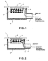
- Figure 1 shows a cooling mechanism according to a first embodiment of the present invention.
- Figure 1 illustrates the structure for controlling a radiation plate temperature on the basis of heat of vaporization of water.
- Water which is temperature controlled to about the same temperature of the structure 110 and 211 ( Figure 5) which constitutes a positioning device, that is, usually about 23 °C, is supplied to a porous material member 2 through a flowpassage 6.
- the porous material member 2 is disposed inside a container 3 which is vacuum exhausted by means of a vacuum pump, for example.
- the water supplied therein is dispersed within the porous material member 2 and, when a vapor pressure (or steam pressure) or lower pressure is reached, vaporization occurs.
- the vapor pressure of water at 0 °C is 610 Pa and, therefore, by keeping the inside pressure of the container 3 at about 100 Pa, the water can be well vaporized even if the temperature of the porous material member 2 comes near to 0 °C.
- the water deprives vaporization heat from the porous material member 2 by 2440 J per 1 g.
- the temperature of the porous material member 2 gradually decreases and, thus, the temperature of a radiation plate 1 connected thereto is lowered. Therefore, even if the temperature of the water to be supplied is at an ordinary temperature, it is possible to decrease the temperature of the radiation plate to about 0 °C.
- the inside pressure of the container 3 is so controlled that the vapor pressure of the water is reached therein at the set temperature of the radiation plate 1, it enables such control cycle that, as the temperature of the radiation plate is lowered and it reaches the set temperature, vaporization of water stops, whereas when the temperature of the radiation plate 1 increases beyond the set temperature, vaporization of water resumes, whereby the temperature of the radiation plate 1 is automatically controlled at the set temperature.
- the temperature precision of the radiation plate 1 or the response of temperature control is taken into account, the inside pressure of the container 3 is made sufficient small (not greater than 100 Pa) and, for the temperature control of the radiation plate 1, heating means such as a heater, for example, provided for the radiation plate 1 is used.
- heating means such as a heater, for example, provided for the radiation plate 1 is used.
- energization (on/off control or applied voltage) of a heater 4 disposed adjacent the radiation plate (at the back of radiation plate in the illustrated example) may be controlled.
- this cooling mechanism is used in an electron beam exposure apparatus, for example, a change in magnetic field due to variation of the electric current flowing through the heater may have an adverse influence.
- the heater is made of a strand structure of high resistance wire material so that the magnetic field produced from the electric current flowing through the wire material can be cancelled. Furthermore, in order to prevent overcooling of peripheral components by the radiation plate 1, an insulating material 5 is provided between the radiation plate 1 and the peripheral structure to thereby suppress the heat transfer.
- any other coolant may be chosen from the standpoint of desired temperature, cooling rate, convenience in usage, for example.
- ammonia may be used as a coolant.
- the set temperature of the radiation plate 1 is not higher than 0 °C, if water is chosen as the coolant, the water may be solidified in the flowpassage 6 inside the porous material member 2. This can be avoided by using ammonia having low solidification temperature.
- the steam pressure of ammonia namely, the pressure of vaporization
- the steam pressure of ammonia is higher than that of water, and it is 4.3 atm at 0 °C and 8.5 atm at 20 °C. Therefore, by supplying ammonia up to the porous material member at a very high supply pressure of 10 atm and by opening the container to the atmosphere (without exhausting it even to vacuum) to hold a pressure of about 1 atm, vaporization phenomenon well occurs and the cooling of the radiation plate is enabled.
- the inside pressure of the container is not always negative, and it may be a positive pressure.
- the temperature of the radiation plate can be held at low temperature, like the case where a Peltier device 201 is used. Therefore, even in an environment wherein any Peltier device is unusable for any magnetic factor or the like, a cooling mechanism having a similar cooling effect can be incorporated into the positioning device. Therefore, radiation cooling even for an electron beam exposure apparatus, for example, can be achieved.
- a radiation plate is taken as a subject of cooling.
- any other cooling subject may be taken.
- the subject of application of this cooling mechanism is not limited to a positioning device as described above.
- a heat pipe is an example using vaporization heat
- Japanese Patent No. 2975089 proposes an exposure apparatus using such mechanism.
- the heat pipe is such structure that a coolant confined in a closed space is vaporized, for cooling, in a higher-temperature region A of the container surface (usually, it is adjacent the subject of cooling) and then it is liquefied in a lower-temperature region (usually, it is a region cooled by a coolant) to emit heat.
- the heat pipe itself is not a cooling mechanism, but rather it is a mechanism for efficiently transmitting heat from the region A to the region B.
- FIG. 2 shows a second embodiment of the present invention.
- This embodiment differs from the first embodiment in that water (coolant) is circulated through a porous material member 2 and that a portion of the circulated water is vaporized through the porous material member 2.
- a positioning device may be equipped with circulation of water for cooling. Thus, a portion of such circulation water may be bypassed toward the porous material member 2.
- the liquid pressure control is easy, and that the liquid is not easily solidified within the flowpassage 6 even if the set radiation plate temperature is low.
- FIG. 3 shows a third embodiment of the present invention.
- a liquid is directly applied against the back of a radiation plate. More specifically, water being supplied through a flowpassage 6 is applied (or discharged) from a nozzle 7 directly against the back of a radiation plate 1. Since the inside pressure of a vacuum container 3 is held by means of a vacuum pump (not shown), for example, at a pressure sufficiently smaller than the steam pressure of the water, the discharged water is vaporized while depriving, from the radiation plate, a heat quantity corresponding to the vaporization heat. With this arrangement, the radiation plate 1 can be cooled, and the temperature thereof can be reduced to about 0 °C.
- the temperature control for the radiation plate may be carried out by controlling energization of a heater 4 provided adjacent the radiation plate (at the back of the radiation plate, in the illustrated example), on the basis of an output of a temperature sensor 8. Furthermore, if it is desired to change the cooling rate based on evaporation heat cooling, it may be effective to intentionally change the amount of discharge of water from the nozzle 7. In order to prevent thermal external disturbance to the radiation plate, an insulating material 5 is provided between the radiation plate and the peripheral structure.
- the water to be supplied to the nozzle 7 it is not specifically necessary to keep the same at low temperature. It may be at the same temperature (usually, about 23 °C) of the peripheral structure. Thus, without changing the structure temperature, the radiation plate can be maintained at low temperature, and so degradation of positioning precision due to thermal deformation is not a problem to be cared.
- the required function of the nozzle 7 is just to discharge a coolant against the subject of cooling. It does not need a particular structure.
- a simple nozzle which uses a pressure difference between the flowpassage 6 and the inside of the container 3, may be used or, alternatively, a nozzle having an inside heat generating element for boiling the water to thereby discharge the same, may be used.
- a nozzle having an inside piezoelectric device or the like for discharging water may be used.
- FIG 4 shows a fourth embodiment of the present invention. While this embodiment has a basic stage structure similar to the Figure 5 structure, the cooling mechanism does not use radiation cooling but it is arranged to directly cool a chuck 113 by using vaporization heat. More specifically, water discharged from a nozzle 7 is directly applied against a chuck 113 which is the subject of cooling, and by vaporization of the water 9 adhered to the chuck surface, the chuck 113 is cooled. The inside pressure of a container 3 is exhausted and maintained by means of a vacuum pump (not shown), for example, at a pressure (about 100 Pa) corresponding to the steam pressure of the water.
- a vacuum pump not shown
- the chuck 113 functions as a portion of the vacuum container 3, and it is disposed opposed to a non-contact seal member 10 provided on the container body, 3 with a small clearance intervening therebetween. With this arrangement, vibration or heat of a rough-motion stage 110 is prevented from being transmitted to the chuck. Additionally, because of vacuum seal effect of the small clearance, there occurs almost no leakage of a gas inside the container 3 to the vacuum ambience around the stage.
- additional temperature control may be made by use of chuck heating means 14 such as a heater, for example, on the basis of an output of a temperature sensor 8 provided to the chuck 113.
- the cooling rate may be controlled by controlling the amount of'water discharge from the nozzle 7.
- a cooling mechanism using vaporization heat of coolant can be applied to a positioning device, with substantially the same cooling effect as attainable with Peltier device. It is therefore possible to meet electron beam exposure apparatus or the like wherein use of Peltier device is difficult.
- the cooling mechanism is incorporated into a positioning device in an electron beam exposure apparatus or the like, high precision positioning and thus high precision exposure as well are assured.
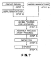
- Step 7 is a flow chart for explaining the procedure of manufacturing various microdevices such as semiconductor chips (e.g., ICs or LSIs), liquid crystal panels, CCDs, thin film magnetic heads or micro-machines, for example.
- Step 1 is a design process for designing a circuit of a semiconductor device.
- Step 2 is a process for making a mask on the basis of the circuit pattern design.
- Step 3 is a process for preparing a wafer by using a material such as silicon.
- Step 4 is a wafer process which is called a pre-process wherein, by using the thus prepared mask and wafer, a circuit is formed on the wafer in practice, in accordance with lithography.
- Step 5 subsequent to this is an assembling step which is called a post-process wherein the wafer having been processed at step 4 is formed into semiconductor chips.
- This step includes an assembling (dicing and bonding) process and a packaging (chip sealing) process.
- Step 6 is an inspection step wherein an operation check, a durability check an so on, for the semiconductor devices produced by step 5, are carried out. With these processes, semiconductor devices are produced, and they are shipped (step 7).
- Step 8 is a flow chart for explaining details of the wafer process.
- Step 11 is an oxidation process for oxidizing the surface of a wafer.
- Step 12 is a CVD process for forming an insulating film on the wafer surface.
- Step 13 is an electrode forming process for forming electrodes upon the wafer by vapor deposition.
- Step 14 is an ion implanting process for implanting ions to the wafer.
- Step 15 is a resist process for applying a resist (photosensitive material) to the wafer.
- Step 16 is an exposure process for printing, by exposure, the circuit pattern of the mask on the wafer through the exposure apparatus described above.
- Step 17 is a developing process for developing the exposed wafer.
- Step 18 is an etching process for removing portions other than the developed resist image.
- Step 19 is a resist separation process for separating the resist material remaining on the wafer after being subjected to the etching process. By repeating these processes, circuit patterns are superposedly formed on the wafer.
- Figure 9 shows a semiconductor device manufacturing exposure apparatus in which a positioning device as described hereinbefore is incorporated as a wafer stage.
- This exposure apparatus is to be used for manufacture of microdevices having a fine pattern formed thereon, such as semiconductor devices (semiconductor integrated circuits, for example), micromachines, or thin-film magnetic heads, for example.
- exposure light which may include visible light, ultraviolet light, EUV light, X-ray, electron beam, and charged particle beam, for example
- a light source 61 illuminates a reticle R (original), and light from the reticle R is projected onto a semiconductor wafer W (substrate) through a projection system having a projection lens 62 (which may include refractive lens, reflective lens, catadioptric lens system, and charged particle lens, for example), whereby a desired pattern is produced on the substrate.
- a projection lens 62 which may include refractive lens, reflective lens, catadioptric lens system, and charged particle lens, for example
- the exposure apparatus includes a base table 51 having a guide 52 and a linear motor stator 21 fixed thereto.
- the linear motor stator 21 has a multiple-phase electromagnetic coil, while a linear motor movable element 11 includes a permanent magnet group.
- the linear motor movable portion 11 is connected as a movable portion 53 to a movable guide 54 (stage), and through the drive of the linear motor M1, the movable guide 54 can be moved in a direction of a normal to the sheet of the drawing.
- the movable portion 53 is supported by a static bearing 55, taking the upper surface of the base table 51 as a reference. and also by a static bearing 56, taking the side surface of the guide 52 as a reference.
- a movable stage 57 which is a stage member disposed to straddle the movable guide 54 is supported by a static bearing 58.
- This movable stage 57 is driven by a similar linear motor M2, so that the movable stage 57 moves leftwardly and rightwardly as viewed in the drawing, while taking the movable guide 54 as a reference.
- the motion of the movable stage 57 is measured by means of an interferometer 60 and a mirror 59 which is fixed to the movable stage 59.
- a wafer (substrate) W is held on a chuck which is mounted on the movable stage 57, and a pattern of the reticle R is transferred in a reduced scale onto different regions on the wafer W by means of the light source 61 and the projection optical system 62, in accordance with a step-and-repeat method or a step-and-scan method.
- the positioning device described hereinbefore can be similarly applied also to an exposure apparatus in which, without using a mask, a circuit pattern is directly drawn on a semiconductor wafer to expose a resist thereon.
- a subject of cooling and/or a cooling member may be provided inside a container or it may be structured as a portion of the container (Item (5) above) and, by vacuum exhausting the container, a cooling device (Item (18) above) can be provided.
- the container may not be completely closed, and it may include a portion which is defined by a structure having members opposed to each other with a small clearance intervening therebetween. Because of seal effect of the small clearance, the function as a container can still be kept, and also since the physical connection between the members is disconnected, thermal insulation and vibration insulation are achieved.
- this advantage of cooling mechanism is best made use of. Particularly, this cooling mechanism is suited to an electron beam exposure apparatus.
Landscapes
- Physics & Mathematics (AREA)
- General Physics & Mathematics (AREA)
- Health & Medical Sciences (AREA)
- Life Sciences & Earth Sciences (AREA)
- Atmospheric Sciences (AREA)
- Toxicology (AREA)
- Engineering & Computer Science (AREA)
- Environmental & Geological Engineering (AREA)
- Epidemiology (AREA)
- Public Health (AREA)
- Exposure And Positioning Against Photoresist Photosensitive Materials (AREA)
- Electron Beam Exposure (AREA)
Applications Claiming Priority (2)
| Application Number | Priority Date | Filing Date | Title |
|---|---|---|---|
| JP2003344012A JP3814598B2 (ja) | 2003-10-02 | 2003-10-02 | 温度調整装置、露光装置及びデバイス製造方法 |
| JP2003344012 | 2003-10-02 |
Publications (3)
| Publication Number | Publication Date |
|---|---|
| EP1521121A2 true EP1521121A2 (de) | 2005-04-06 |
| EP1521121A3 EP1521121A3 (de) | 2006-05-17 |
| EP1521121B1 EP1521121B1 (de) | 2013-07-03 |
Family
ID=34309129
Family Applications (1)
| Application Number | Title | Priority Date | Filing Date |
|---|---|---|---|
| EP04256106.8A Expired - Lifetime EP1521121B1 (de) | 2003-10-02 | 2004-10-01 | Kühltechnik |
Country Status (3)
| Country | Link |
|---|---|
| US (1) | US20050092013A1 (de) |
| EP (1) | EP1521121B1 (de) |
| JP (1) | JP3814598B2 (de) |
Cited By (5)
| Publication number | Priority date | Publication date | Assignee | Title |
|---|---|---|---|---|
| WO2008004646A1 (en) * | 2006-07-01 | 2008-01-10 | Nikon Corporation | Exposure apparatus that includes a phase change circulation system for movers |
| WO2010015511A1 (en) * | 2008-08-08 | 2010-02-11 | Asml Netherlands B.V. | Lithographic apparatus and device manufacturing method |
| CN102445856A (zh) * | 2011-10-12 | 2012-05-09 | 上海华力微电子有限公司 | 一种光刻机硅片载物台温度控制系统及其控制方法 |
| CN103163746A (zh) * | 2011-12-08 | 2013-06-19 | 上海微电子装备有限公司 | 一种具有温度探测功能的掩模对准探测器、光刻装置及对准探测方法 |
| EP3832391A1 (de) * | 2019-12-03 | 2021-06-09 | ASML Netherlands B.V. | Klemmanordnung |
Families Citing this family (20)
| Publication number | Priority date | Publication date | Assignee | Title |
|---|---|---|---|---|
| JP4418699B2 (ja) * | 2004-03-24 | 2010-02-17 | キヤノン株式会社 | 露光装置 |
| JP2006287014A (ja) * | 2005-04-01 | 2006-10-19 | Canon Inc | 位置決め装置およびリニアモータ |
| JP2007027632A (ja) * | 2005-07-21 | 2007-02-01 | Nikon Corp | 光学装置及び露光装置、並びにデバイス製造方法 |
| JP2008528934A (ja) * | 2006-01-11 | 2008-07-31 | ビ−エイイ− システムズ パブリック リミテッド カンパニ− | 冷却剤送出に関する改良 |
| JP5020662B2 (ja) * | 2006-05-26 | 2012-09-05 | キヤノン株式会社 | ステージ装置、露光装置、及びデバイス製造方法 |
| US7528349B1 (en) | 2006-07-25 | 2009-05-05 | Kla-Tencor Technologies Corporation | Temperature stabilization for substrate processing |
| US7633070B2 (en) * | 2006-12-18 | 2009-12-15 | Kla-Tencor Technologies Corporation | Substrate processing apparatus and method |
| US8058628B2 (en) * | 2007-07-09 | 2011-11-15 | Kla-Tencor Corporation | Substrate processing apparatus and method |
| US7897942B1 (en) | 2007-12-20 | 2011-03-01 | Kla-Tencor Corporation | Dynamic tracking of wafer motion and distortion during lithography |
| JP5651317B2 (ja) * | 2009-03-31 | 2015-01-07 | 東京エレクトロン株式会社 | 半導体製造装置及び温調方法 |
| JP5601800B2 (ja) * | 2009-07-16 | 2014-10-08 | 株式会社テイエルブイ | 気化冷却装置 |
| JP2011226662A (ja) * | 2010-04-15 | 2011-11-10 | Tlv Co Ltd | 加熱冷却装置 |
| JP2011226663A (ja) * | 2010-04-15 | 2011-11-10 | Tlv Co Ltd | 冷却装置 |
| WO2012008840A2 (en) * | 2010-07-16 | 2012-01-19 | Screenyard B.V. | Cooling element |
| JP5762704B2 (ja) * | 2010-08-20 | 2015-08-12 | 東京エレクトロン株式会社 | 基板処理装置及び温度調節方法 |
| JP5896549B2 (ja) * | 2011-07-20 | 2016-03-30 | 株式会社ダイヘン | 冷却ユニット及びこれを用いたワーク搬送装置 |
| TW201518538A (zh) * | 2013-11-11 | 2015-05-16 | 應用材料股份有限公司 | 像素化冷卻溫度控制的基板支撐組件 |
| US10691013B2 (en) | 2013-12-22 | 2020-06-23 | Applied Materials, Inc. | Extreme ultraviolet lithography system having chuck assembly and method of manufacturing thereof |
| CN108507227B (zh) * | 2018-04-20 | 2024-05-07 | 宁波瑞凌新能源科技有限公司 | 一种利用辐射制冷的冷却水系统 |
| JP7008675B2 (ja) * | 2019-10-15 | 2022-01-25 | 日本電子株式会社 | 荷電粒子線装置用冷却装置 |
Citations (2)
| Publication number | Priority date | Publication date | Assignee | Title |
|---|---|---|---|---|
| US5413167A (en) | 1990-07-30 | 1995-05-09 | Canon Kabushiki Kaisha | Wafer cooling device |
| JPH07226371A (ja) | 1994-02-14 | 1995-08-22 | Dainippon Screen Mfg Co Ltd | 基板冷却装置 |
Family Cites Families (19)
| Publication number | Priority date | Publication date | Assignee | Title |
|---|---|---|---|---|
| US4730665A (en) * | 1983-07-14 | 1988-03-15 | Technology Enterprises Company | Apparatus for cooling high-density integrated circuit packages |
| JPH01104349A (ja) * | 1987-10-15 | 1989-04-21 | Nippon Telegr & Teleph Corp <Ntt> | 真空容器内極低温ステージ |
| USH1145H (en) * | 1990-09-25 | 1993-03-02 | Sematech, Inc. | Rapid temperature response wafer chuck |
| DE69118315T2 (de) * | 1990-11-01 | 1996-08-14 | Canon Kk | Waferhaltebefestigung für Belichtungsgerät |
| US5775416A (en) * | 1995-11-17 | 1998-07-07 | Cvc Products, Inc. | Temperature controlled chuck for vacuum processing |
| JPH11307430A (ja) * | 1998-04-23 | 1999-11-05 | Canon Inc | 露光装置およびデバイス製造方法ならびに駆動装置 |
| JP3870002B2 (ja) * | 2000-04-07 | 2007-01-17 | キヤノン株式会社 | 露光装置 |
| JP4383626B2 (ja) * | 2000-04-13 | 2009-12-16 | キヤノン株式会社 | 位置決め装置および露光装置 |
| US7082778B2 (en) * | 2001-02-22 | 2006-08-01 | Hewlett-Packard Development Company, L.P. | Self-contained spray cooling module |
| JP2002280283A (ja) * | 2001-03-16 | 2002-09-27 | Canon Inc | 基板処理装置 |
| EP1276016B1 (de) * | 2001-07-09 | 2009-06-10 | Canon Kabushiki Kaisha | Belichtungsapparat |
| JP4745556B2 (ja) * | 2001-08-20 | 2011-08-10 | キヤノン株式会社 | 位置決め装置、露光装置、及びデバイス製造方法 |
| JP2004146492A (ja) * | 2002-10-23 | 2004-05-20 | Canon Inc | Euv露光装置 |
| US6936551B2 (en) * | 2002-05-08 | 2005-08-30 | Applied Materials Inc. | Methods and apparatus for E-beam treatment used to fabricate integrated circuit devices |
| US20040101632A1 (en) * | 2002-11-22 | 2004-05-27 | Applied Materials, Inc. | Method for curing low dielectric constant film by electron beam |
| US6745575B2 (en) * | 2002-07-11 | 2004-06-08 | Temptronic Corporation | Workpiece chuck with temperature control assembly having spacers between layers providing clearance for thermoelectric modules |
| JP2004159493A (ja) * | 2002-10-16 | 2004-06-03 | Nikon Corp | リニアモータ装置、ステージ装置及び露光装置並びにリニアモータ装置の冷却方法 |
| US6827135B1 (en) * | 2003-06-12 | 2004-12-07 | Gary W. Kramer | High flux heat removal system using jet impingement of water at subatmospheric pressure |
| US7310230B2 (en) * | 2003-08-21 | 2007-12-18 | Delta Design, Inc. | Temperature control system which sprays liquid coolant droplets against an IC-module at a sub-atmospheric pressure |
-
2003
- 2003-10-02 JP JP2003344012A patent/JP3814598B2/ja not_active Expired - Fee Related
-
2004
- 2004-10-01 US US10/954,276 patent/US20050092013A1/en not_active Abandoned
- 2004-10-01 EP EP04256106.8A patent/EP1521121B1/de not_active Expired - Lifetime
Patent Citations (2)
| Publication number | Priority date | Publication date | Assignee | Title |
|---|---|---|---|---|
| US5413167A (en) | 1990-07-30 | 1995-05-09 | Canon Kabushiki Kaisha | Wafer cooling device |
| JPH07226371A (ja) | 1994-02-14 | 1995-08-22 | Dainippon Screen Mfg Co Ltd | 基板冷却装置 |
Cited By (14)
| Publication number | Priority date | Publication date | Assignee | Title |
|---|---|---|---|---|
| WO2008004646A1 (en) * | 2006-07-01 | 2008-01-10 | Nikon Corporation | Exposure apparatus that includes a phase change circulation system for movers |
| CN102067039B (zh) * | 2008-08-08 | 2014-04-09 | Asml荷兰有限公司 | 光刻设备和器件制造方法 |
| WO2010015511A1 (en) * | 2008-08-08 | 2010-02-11 | Asml Netherlands B.V. | Lithographic apparatus and device manufacturing method |
| CN102067039A (zh) * | 2008-08-08 | 2011-05-18 | Asml荷兰有限公司 | 光刻设备和器件制造方法 |
| US8994917B2 (en) | 2008-08-08 | 2015-03-31 | Asml Netherlands B.V. | Temperature stabilization system to stabilize a temperature of an article |
| CN102445856B (zh) * | 2011-10-12 | 2014-12-10 | 上海华力微电子有限公司 | 一种光刻机硅片载物台温度控制系统及其控制方法 |
| CN102445856A (zh) * | 2011-10-12 | 2012-05-09 | 上海华力微电子有限公司 | 一种光刻机硅片载物台温度控制系统及其控制方法 |
| CN103163746A (zh) * | 2011-12-08 | 2013-06-19 | 上海微电子装备有限公司 | 一种具有温度探测功能的掩模对准探测器、光刻装置及对准探测方法 |
| CN103163746B (zh) * | 2011-12-08 | 2015-09-30 | 上海微电子装备有限公司 | 一种具有温度探测功能的掩模对准探测器、光刻装置及对准探测方法 |
| CN103163746B8 (zh) * | 2011-12-08 | 2016-07-13 | 上海微电子装备有限公司 | 一种具有温度探测功能的掩模对准探测器、光刻装置及对准探测方法 |
| EP3832391A1 (de) * | 2019-12-03 | 2021-06-09 | ASML Netherlands B.V. | Klemmanordnung |
| WO2021110336A1 (en) * | 2019-12-03 | 2021-06-10 | Asml Netherlands B.V. | Clamp assembly |
| TWI864165B (zh) * | 2019-12-03 | 2024-12-01 | 荷蘭商Asml荷蘭公司 | 夾具總成及使夾具之下部基底表面放電之方法 |
| US12189309B2 (en) | 2019-12-03 | 2025-01-07 | Asml Netherlands B.V. | Clamp assembly |
Also Published As
| Publication number | Publication date |
|---|---|
| JP2005109375A (ja) | 2005-04-21 |
| JP3814598B2 (ja) | 2006-08-30 |
| US20050092013A1 (en) | 2005-05-05 |
| EP1521121B1 (de) | 2013-07-03 |
| EP1521121A3 (de) | 2006-05-17 |
Similar Documents
| Publication | Publication Date | Title |
|---|---|---|
| EP1521121B1 (de) | Kühltechnik | |
| US20040244963A1 (en) | Heat pipe with temperature control | |
| CN1890607B (zh) | 平版印刷系统中的有用物传送系统 | |
| US20050212362A1 (en) | Linear motor, stage apparatus, exposure apparatus, and device manufacturing method | |
| US8994917B2 (en) | Temperature stabilization system to stabilize a temperature of an article | |
| US8976333B2 (en) | Lithographic apparatus and lithographic apparatus cooling method | |
| EP1548503B1 (de) | Lithographischer Apparat | |
| US7106416B2 (en) | Lithographic apparatus and device manufacturing method | |
| US20040165161A1 (en) | Cooling mechanism | |
| JP2004146492A (ja) | Euv露光装置 | |
| US20020124993A1 (en) | Apparatus with air-conditioning system, and device manufacturing method using the same | |
| US7164466B2 (en) | Detachable heat sink | |
| US20100186942A1 (en) | Reticle error reduction by cooling | |
| US20070114655A1 (en) | Apparatus for cooling | |
| JP2005295762A (ja) | ステージ装置および露光装置 | |
| US7460213B2 (en) | Alignment apparatus, exposure apparatus, and device manufacturing method using exposure apparatus | |
| JP2001023890A (ja) | 露光装置およびこれを用いたデバイス製造方法 | |
| JP2002186242A (ja) | 電磁アクチュエータ装置、ステージ装置、露光装置及びデバイス |
Legal Events
| Date | Code | Title | Description |
|---|---|---|---|
| PUAI | Public reference made under article 153(3) epc to a published international application that has entered the european phase |
Free format text: ORIGINAL CODE: 0009012 |
|
| AK | Designated contracting states |
Kind code of ref document: A2 Designated state(s): AT BE BG CH CY CZ DE DK EE ES FI FR GB GR HU IE IT LI LU MC NL PL PT RO SE SI SK TR |
|
| AX | Request for extension of the european patent |
Extension state: AL HR LT LV MK |
|
| PUAL | Search report despatched |
Free format text: ORIGINAL CODE: 0009013 |
|
| AK | Designated contracting states |
Kind code of ref document: A3 Designated state(s): AT BE BG CH CY CZ DE DK EE ES FI FR GB GR HU IE IT LI LU MC NL PL PT RO SE SI SK TR |
|
| AX | Request for extension of the european patent |
Extension state: AL HR LT LV MK |
|
| 17P | Request for examination filed |
Effective date: 20061117 |
|
| AKX | Designation fees paid |
Designated state(s): DE GB NL |
|
| 17Q | First examination report despatched |
Effective date: 20110225 |
|
| GRAP | Despatch of communication of intention to grant a patent |
Free format text: ORIGINAL CODE: EPIDOSNIGR1 |
|
| RIN1 | Information on inventor provided before grant (corrected) |
Inventor name: EMOTO, KEIJI, |
|
| GRAS | Grant fee paid |
Free format text: ORIGINAL CODE: EPIDOSNIGR3 |
|
| GRAA | (expected) grant |
Free format text: ORIGINAL CODE: 0009210 |
|
| AK | Designated contracting states |
Kind code of ref document: B1 Designated state(s): DE GB NL |
|
| REG | Reference to a national code |
Ref country code: GB Ref legal event code: FG4D |
|
| REG | Reference to a national code |
Ref country code: DE Ref legal event code: R096 Ref document number: 602004042588 Country of ref document: DE Effective date: 20130829 |
|
| REG | Reference to a national code |
Ref country code: NL Ref legal event code: T3 |
|
| PGFP | Annual fee paid to national office [announced via postgrant information from national office to epo] |
Ref country code: DE Payment date: 20131031 Year of fee payment: 10 |
|
| PGFP | Annual fee paid to national office [announced via postgrant information from national office to epo] |
Ref country code: NL Payment date: 20131015 Year of fee payment: 10 |
|
| PLBE | No opposition filed within time limit |
Free format text: ORIGINAL CODE: 0009261 |
|
| STAA | Information on the status of an ep patent application or granted ep patent |
Free format text: STATUS: NO OPPOSITION FILED WITHIN TIME LIMIT |
|
| 26N | No opposition filed |
Effective date: 20140404 |
|
| GBPC | Gb: european patent ceased through non-payment of renewal fee |
Effective date: 20131003 |
|
| REG | Reference to a national code |
Ref country code: DE Ref legal event code: R097 Ref document number: 602004042588 Country of ref document: DE Effective date: 20140404 |
|
| PG25 | Lapsed in a contracting state [announced via postgrant information from national office to epo] |
Ref country code: GB Free format text: LAPSE BECAUSE OF NON-PAYMENT OF DUE FEES Effective date: 20131003 |
|
| REG | Reference to a national code |
Ref country code: DE Ref legal event code: R119 Ref document number: 602004042588 Country of ref document: DE |
|
| REG | Reference to a national code |
Ref country code: NL Ref legal event code: V1 Effective date: 20150501 |
|
| PG25 | Lapsed in a contracting state [announced via postgrant information from national office to epo] |
Ref country code: DE Free format text: LAPSE BECAUSE OF NON-PAYMENT OF DUE FEES Effective date: 20150501 |
|
| PG25 | Lapsed in a contracting state [announced via postgrant information from national office to epo] |
Ref country code: NL Free format text: LAPSE BECAUSE OF NON-PAYMENT OF DUE FEES Effective date: 20150501 |