EP1519640B1 - Verfahren zur Herstellung einer flexiblen Leiterplatte - Google Patents
Verfahren zur Herstellung einer flexiblen Leiterplatte Download PDFInfo
- Publication number
- EP1519640B1 EP1519640B1 EP04023035A EP04023035A EP1519640B1 EP 1519640 B1 EP1519640 B1 EP 1519640B1 EP 04023035 A EP04023035 A EP 04023035A EP 04023035 A EP04023035 A EP 04023035A EP 1519640 B1 EP1519640 B1 EP 1519640B1
- Authority
- EP
- European Patent Office
- Prior art keywords
- elongate substrate
- circuit board
- conductive pattern
- wired circuit
- flexible wired
- Prior art date
- Legal status (The legal status is an assumption and is not a legal conclusion. Google has not performed a legal analysis and makes no representation as to the accuracy of the status listed.)
- Expired - Lifetime
Links
Images


Classifications
-
- H—ELECTRICITY
- H05—ELECTRIC TECHNIQUES NOT OTHERWISE PROVIDED FOR
- H05K—PRINTED CIRCUITS; CASINGS OR CONSTRUCTIONAL DETAILS OF ELECTRIC APPARATUS; MANUFACTURE OF ASSEMBLAGES OF ELECTRICAL COMPONENTS
- H05K3/00—Apparatus or processes for manufacturing printed circuits
- H05K3/0097—Processing two or more printed circuits simultaneously, e.g. made from a common substrate, or temporarily stacked circuit boards
-
- H—ELECTRICITY
- H05—ELECTRIC TECHNIQUES NOT OTHERWISE PROVIDED FOR
- H05K—PRINTED CIRCUITS; CASINGS OR CONSTRUCTIONAL DETAILS OF ELECTRIC APPARATUS; MANUFACTURE OF ASSEMBLAGES OF ELECTRICAL COMPONENTS
- H05K3/00—Apparatus or processes for manufacturing printed circuits
- H05K3/22—Secondary treatment of printed circuits
-
- H—ELECTRICITY
- H05—ELECTRIC TECHNIQUES NOT OTHERWISE PROVIDED FOR
- H05K—PRINTED CIRCUITS; CASINGS OR CONSTRUCTIONAL DETAILS OF ELECTRIC APPARATUS; MANUFACTURE OF ASSEMBLAGES OF ELECTRICAL COMPONENTS
- H05K3/00—Apparatus or processes for manufacturing printed circuits
- H05K3/007—Manufacture or processing of a substrate for a printed circuit board supported by a temporary or sacrificial carrier
-
- H—ELECTRICITY
- H05—ELECTRIC TECHNIQUES NOT OTHERWISE PROVIDED FOR
- H05K—PRINTED CIRCUITS; CASINGS OR CONSTRUCTIONAL DETAILS OF ELECTRIC APPARATUS; MANUFACTURE OF ASSEMBLAGES OF ELECTRICAL COMPONENTS
- H05K3/00—Apparatus or processes for manufacturing printed circuits
- H05K3/02—Apparatus or processes for manufacturing printed circuits in which the conductive material is applied to the surface of the insulating support and is thereafter removed from such areas of the surface which are not intended for current conducting or shielding
- H05K3/06—Apparatus or processes for manufacturing printed circuits in which the conductive material is applied to the surface of the insulating support and is thereafter removed from such areas of the surface which are not intended for current conducting or shielding the conductive material being removed chemically or electrolytically, e.g. by photo-etch process
-
- H—ELECTRICITY
- H05—ELECTRIC TECHNIQUES NOT OTHERWISE PROVIDED FOR
- H05K—PRINTED CIRCUITS; CASINGS OR CONSTRUCTIONAL DETAILS OF ELECTRIC APPARATUS; MANUFACTURE OF ASSEMBLAGES OF ELECTRICAL COMPONENTS
- H05K1/00—Printed circuits
- H05K1/02—Details
- H05K1/03—Use of materials for the substrate
- H05K1/0393—Flexible materials
-
- H—ELECTRICITY
- H05—ELECTRIC TECHNIQUES NOT OTHERWISE PROVIDED FOR
- H05K—PRINTED CIRCUITS; CASINGS OR CONSTRUCTIONAL DETAILS OF ELECTRIC APPARATUS; MANUFACTURE OF ASSEMBLAGES OF ELECTRICAL COMPONENTS
- H05K2203/00—Indexing scheme relating to apparatus or processes for manufacturing printed circuits covered by H05K3/00
- H05K2203/01—Tools for processing; Objects used during processing
- H05K2203/0147—Carriers and holders
- H05K2203/0156—Temporary polymeric carrier or foil, e.g. for processing or transferring
-
- H—ELECTRICITY
- H05—ELECTRIC TECHNIQUES NOT OTHERWISE PROVIDED FOR
- H05K—PRINTED CIRCUITS; CASINGS OR CONSTRUCTIONAL DETAILS OF ELECTRIC APPARATUS; MANUFACTURE OF ASSEMBLAGES OF ELECTRICAL COMPONENTS
- H05K2203/00—Indexing scheme relating to apparatus or processes for manufacturing printed circuits covered by H05K3/00
- H05K2203/15—Position of the PCB during processing
- H05K2203/1545—Continuous processing, i.e. involving rolls moving a band-like or solid carrier along a continuous production path
-
- H—ELECTRICITY
- H05—ELECTRIC TECHNIQUES NOT OTHERWISE PROVIDED FOR
- H05K—PRINTED CIRCUITS; CASINGS OR CONSTRUCTIONAL DETAILS OF ELECTRIC APPARATUS; MANUFACTURE OF ASSEMBLAGES OF ELECTRICAL COMPONENTS
- H05K3/00—Apparatus or processes for manufacturing printed circuits
- H05K3/10—Apparatus or processes for manufacturing printed circuits in which conductive material is applied to the insulating support in such a manner as to form the desired conductive pattern
- H05K3/108—Apparatus or processes for manufacturing printed circuits in which conductive material is applied to the insulating support in such a manner as to form the desired conductive pattern by semi-additive methods; masks therefor
-
- H—ELECTRICITY
- H05—ELECTRIC TECHNIQUES NOT OTHERWISE PROVIDED FOR
- H05K—PRINTED CIRCUITS; CASINGS OR CONSTRUCTIONAL DETAILS OF ELECTRIC APPARATUS; MANUFACTURE OF ASSEMBLAGES OF ELECTRICAL COMPONENTS
- H05K3/00—Apparatus or processes for manufacturing printed circuits
- H05K3/22—Secondary treatment of printed circuits
- H05K3/28—Applying non-metallic protective coatings
Definitions
- the present invention relates to a producing method of a flexible wired circuit board and, more particularly, to a method of producing a flexible wired circuit board, while an elongate substrate is conveyed using rolls.
- JP Laid-open (Unexamined) Patent Publication No. Hei 6-132628 proposes that a carrier film, such as a polyethylene terephthalate film, is bonded to a surface of a thin, copper clad laminate.
- a current density becomes higher at both widthwise end portions of the elongate substrate than at a central portion of the same.
- thickness of the conductive pattern plated becomes larger at the both widthwise ends of the elongate substrate than at the central portion of the same.
- etching solution or developing solution is entrained into a gap between the carrier sheet and the elongate substrate at both end portions thereof formed by the strip of the carrier sheet from the elongate substrate via the capillary phenomenon. Then, the entrained solution remains through the subsequent processes, causing contamination of the flexible wired circuit board obtained.
- the present invention provides a producing method of a flexible wired circuit board as claimed in claim 1.
- the stiffener sheet is provided on the elongate substrate, with its widthwise edge placed 1-10mm inwardly from widthwise edge of the elongate substrate.
- the elongate substrate has a thickness of 5-50 ⁇ m.
- the stiffener sheet having a width narrower than the elongate substrate is provided on the elongate substrate, the stiffener sheet can be prevented from being stripped off from the both end portions of the elongate substrate.
- the stiffener sheet is prevented from being stripped off from the elongate substrate in the producing processes, while the fine conductive pattern can be formed on the thin, elongate, substrate efficiently by the electrolysis plating.
- This can prevent the occurrence that the etching solution or developing solution entrains into the gap between the stiffener sheet and the elongate substrate via the capillary phenomenon, and as such can prevent the occurrence of contamination of the flexible wired circuit board obtained.
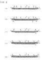
- FIGS. 1 and 2 are the production process drawings showing an embodiment of a producing method of a flexible wired circuit board of the present invention.
- FIG. 3 is a schematic block diagram of the manufacturing equipment used for carrying out the embodiment of the producing method.
- the manufacturing equipment 20 is equipped with a delivery roll 21 and a wind-up roll 22 which are spaced apart at a predetermined distance from each other.
- an elongate substrate 1 rolled on the delivery roll 21 is delivered toward the wind-up roll 22 (in the direction indicated by an arrow 23) and is wound up by the wind-up roll 22, first, and, then, the elongate substrate 1 is rewound from the wind-up roll 22 to the delivery roll 21 (in the direction indicated by an arrow 24).
- These processes are alternately repeated in succession.
- the respective processes shown in FIG. 1(b) through FIG. 2(k) are carried out in sequence.
- the elongate substrate 1 is prepared, first, as shown in FIG. 1(a) .
- the elongate substrate 1 is the one used for forming an insulating base layer of a flexible wired circuit board. Any particular limitation is imposed on the material for the elongate substrate 1, as long as it may be used for the insulating base layer.
- resin sheets resin films
- polyimide resin sheet acrylic resin sheet, polyether nitrile resin sheet, polyether sulfonic resin sheet, polyethylene terephthalate resin sheet, polyethylene naphthalate resin sheet and polyvinyl chloride resin sheet
- polyimide resin sheet is used.
- the elongate substrate 1 has a thickness of e.g. 5-50 ⁇ m, or preferably 10-30 ⁇ m.
- the use of the elongate substrate 1 having a thickness in this order can produce a low-profile flexible wired circuit board. It usually has a width of 100-500mm, or preferably 150-350mm, and a length of 10-1,500m, or preferably 100-300m.
- This elongate substrate 1 is prepared in the form of an elongate sheet in a tape-like form wound up on the delivery roll 21.
- a thin metal film 2 is formed on the entire surface of the elongate substrate 1, as shown in FIG. 1(b) .
- a vacuum deposition process or a sputtering process can be used to form the thin metal film 2.
- the sputtering is used.
- chromium and copper are preferably used as the metal for forming the thin metal film 2.
- a thin chrome film and a thin copper film are formed in sequence on the entire surface of the elongate substrate 1 by the sputtering process.
- the metal film 2 is formed so that the thin chrome film can have thickness of e.g. 5-50nm and the thin copper film can have thickness of e.g. 50-500nm.
- a plating resist 4 of a reversed pattern of the conductive pattern 3 is formed on the thin metal film 2, as shown in FIG. 1(c) .
- the plating resist 4 of the reversed pattern of the conductive pattern 3 is formed on the thin metal film 2 by a known method that a photosensitive dry film resist is bonded to a surface of the thin metal film 2, or liquid photoresist is applied thereto and dried, and then the resultant film is exposed to light and developed.
- the stiffener sheet 5 should preferably be provided on the elongate substrate 1.
- the stiffener sheet 5 is bonded to the back side of the elongate substrate 1 or on the back side thereof opposite to the front side where the plating resist 4 is formed.
- the stiffener sheet 5 can be provided on the elongate substrate 1 in the following manner.
- the same resin sheet (resin film) as the one mentioned above is bonded to the elongate substrate 1 via adhesive.
- the same photosensitive dry film resist as the one mentioned above may be bonded to or the liquid resist mentioned above may applied to the elongate substrate 1 and dried in the same manner as above (except that the resultant film is exposed to light and developed).
- the stiffener sheet 5 has a thickness of e.g. 20-200 ⁇ m or preferably 50-150 ⁇ m, and a width equal to or larger than the elongate substrate 1.
- the conductor layer 3 is formed by electrolysis plating on an area of the thin metal film 2 where the plating resist 4 is not formed, as shown in FIG. 1(d) .
- Any conductive material may be used for forming the conductive pattern 3 without any particular limitation, as long as it can be plated by electrolysis plating.
- copper, nickel, gold, solder, or alloys thereof may be used.
- copper is used.
- the conductive pattern 3 has a thickness of e.g. 5-20 ⁇ m, or preferably 8-12 ⁇ m, at a widthwise center portion thereof as mentioned later.
- the conductive pattern 3 is formed in a fine wired circuit pattern formed by a plurality of lines of wire 6 extending along a longitudinal direction of the elongate substrate 1 and arranged in parallel with each other with a given space.
- Each line of wire 6 usually has a width of 5-50 ⁇ m and an interval between adjacent lines of wire 6 is usually set to be 5-50 ⁇ m.
- this conductive pattern 3 is formed by electrolysis plating, or preferably by electrolysis copper plating, while the elongate substrate 1 passes through a plating bath continuously between the delivery roll 21 and the wind-up roll 22.
- a current density becomes higher at both widthwise(in a direction perpendicular to the longitudinal direction of the elongate substrate 1) end portions of the elongate substrate 1 than at a widthwise central portion of the same.
- the lines of wire 6 of the conductive pattern 3 plated becomes larger in thickness at the both widthwise ends of the elongate substrate 1 than at the widthwise central portion of the same.
- the thickness of the lines of wire 6 at the widthwise central portion of the conductive pattern 3 be 100%, the thickness of the lines of wire 6 at the both widthwise ends of the same becomes 105-150%.
- the plating resist 4 is removed by a known etching process, such as a chemical etching (wet etching), or by stripping, as shown in FIG. 1(e) .
- a known etching process such as a chemical etching (wet etching), or by stripping, as shown in FIG. 1(e) .
- the thin metal film 2 exposed from the conductive pattern 3 is also removed by the known etching process such as the chemical etching (wet etching), as shown in FIG. 1(f) .
- the stiffener sheet 5 is provided on the backside of the elongate substrate 1, then the stiffener sheet 5 is also stripped from the elongate substrate 1. Thereafter, the resultant elongate substrate 1 is wound up on the delivery roll 21 or the wind-up roll 22. Then, the elongate substrate 1 thus wound up is annealed as it is, to crystallize the conductive pattern 3. It is to be noted that as the elongate substrate 1 is wound up on the roll, differences in thickness between the both end portions of the elongate substrate 1 and the central portion of the same are accumulated, so that the elongate substrate 1 is undulated and deformed plastically at the both end portions by the wind up pressure.
- the elongate substrate 1 is annealed by heating at e.g. 150-300°C, or preferably at 180-270°C, for 1-10 hours, or preferably for 2-5 hours. As the result of this annealing, an oxidized film 8 is formed on the surface of the conductive pattern 3, as shown in FIG. 2(g) .
- a stiffener sheet 9 having a width narrower than the elongate substrate 1 is formed on the back side of the elongate substrate 1 on the opposite side to the front side where the conductive pattern 3 is formed, as shown in FIG. 2(h) .
- the stiffener sheet 9 is formed, for example, from the same resin sheet (resin film) as above, or preferably from a polyethylene terephthalate film.
- the resin sheet having a width of e.g. 90-498mm, or preferably 145-345mm, is used as the stiffener sheet 9. Letting the width of the elongate substrate 1 be 100%, the width of the stiffener sheet 9 is preferably in the range of 90.0% to 99.6%, or preferably in the range of 96.7% to 98.6%.
- the stiffener sheet 9 is bonded to the back side of the elongate substrate 1 via known adhesive, for example.
- the stiffener sheet 9 is bonded to the elongate substrate 1 in such a manner as to allow margins 10 at the both end portions of the elongate substrate 1, in order not to overlap with the both end portions of the elongate substrate 1 as were deformed plastically by annealing.
- Each margin 10 is preferably set to have a width of 1-10mm, or preferably 2-5mm.
- the stiffener sheet 9 is bonded to the elongate substrate 1, with its both widthwise edges placed 1-10mm, or preferably 2-5mm, inwardly from the both widthwise edges of the elongate substrate 1.
- the oxidized film 8 on the surface of the conductive pattern 3 is removed, as shown in FIG. 2(i) .
- the oxidized film 8 is removed using the chemical etching (wet etching), for example.
- the oxidized film 8 is removed by soft etching using mixed solution of hydrogen peroxide and nitric acid as an etching solution.
- solder resist 11 is formed to cover the conductive pattern 3, as shown in FIG. 2(j) .
- the solder resist 11 is formed by a photographic method according to which for example liquid solution of photosensitive solder resist is applied to the surface of the elongate substrate 1 including the conductive pattern 3 and then dried, to form a paint film, first, and then the paint film is exposed to light and developed.
- an insulating cover layer to cover the conductive pattern 3 may be formed from photosensitive polyimide resin, for example.
- the stiffener sheet 9 is stripped off from the elongate substrate 1 to obtain a flexible wired circuit board, as shown in FIG. 2(k) .
- the flexible wired circuit board is produced by this method, the following result is obtained. Even when the electrolysis plating for forming the conductive pattern 3 causes the lines of wire 6 of the conductive pattern 3 to be larger in thickness at the both widthwise end portions of the elongate substrate 1 than at the widthwise central portion of the same and in turn causes the elongate substrate 1 to be undulated and deformed plastically at the both widthwise end portions thereof by the wind-up pressure when the elongate substrate 1 is wound up on the delivery roll 21 or the wind-up roll 22, since the stiffener sheet 9 is bonded to the elongate substrate 1 in such a manner as not to overlap with the plastically deformed end portions of the elongate substrate 1 in the subsequent process, the stiffener sheet 9 can be prevented from being stripped off from the both end portions of the elongate substrate 1 when wound up in the subsequent processes.
- the delivery and the rewinding was performed between the wind-up roll and the delivery roll were alternately repeated and, in the course of the delivery or the rewinding, the following processes were carried out in sequence.
- An elongate substrate of a polyimide resin sheet having a width of 250mm and a thickness of 25 ⁇ m was prepared (Cf. FIG. 1(a) ). Then, a thin metal film comprising a thin chromium film having a thickness of 10nm and a thin copper film having a thickness of 200nm was formed on the entire surface of the elongate substrate by the sputtering process (Cf. FIG. 1(b) ).
- a conductor pattern was formed by electrolysis copper plating on an area of the thin metal film where the plating resist was not formed (Cf. FIG. 1(d) ).
- This conductive pattern was formed in a fine wired circuit pattern formed by a plurality of lines of wire extending along a longitudinal direction of the elongate substrate and arranged in parallel with each other with a given space.
- the lines of wire were set to be 25 ⁇ m in width and 25 ⁇ m in the interval between adjacent lines of wire.
- the conductive pattern had a thickness of 12 ⁇ m at both widthwise ends thereof and a thickness of 10 ⁇ m at a widthwise central portion thereof.
- the elongate substrate was annealed in its wound-up state (Cf. FIG. 2(g) ). It was found that the elongate substrate was undulated at the both widthwise end portions when wound up on the roll in the subsequent process.
- the stiffener sheet was bonded to the elongate substrate in such a manner that its both edges are placed 2.5mm inwardly from the both widthwise edges of the elongate substrate (Cf. FIG. 2(h) ).
- liquid solution of a photosensitive solder resist was applied to the surface of the elongate substrate including the conductive pattern and then dried, to form a paint film and then the paint film was exposed to light and developed, to form a solder resist so as to cover the conductive pattern (Cf. FIG. 2(j) ).
- a photosensitive solder resist was applied to the surface of the elongate substrate including the conductive pattern and then dried, to form a paint film and then the paint film was exposed to light and developed, to form a solder resist so as to cover the conductive pattern (Cf. FIG. 2(j) ).
- Example 1 Except that the stiffener sheet to be bonded to the elongate substrate after the annealing having the same width of 252mm as the width of the elongate substrate was used and bonded to the elongate substrate in such a manner as to overlap with it completely, the same method as that of Example 1 was carried out to obtain a flexible wired circuit board.
Landscapes
- Engineering & Computer Science (AREA)
- Manufacturing & Machinery (AREA)
- Microelectronics & Electronic Packaging (AREA)
- Manufacturing Of Printed Circuit Boards (AREA)
- Manufacturing Of Printed Wiring (AREA)
- Structure Of Printed Boards (AREA)
- Non-Metallic Protective Coatings For Printed Circuits (AREA)
Claims (3)
- Herstellungsverfahren für eine flexible verdrahtete Leiterplatte, das aufweist:das Verfahren zur Ausbildung von leitenden Strukturen auf einer Oberfläche eines längserstreckten Substrates (1) durch Elektrolysebeschichtung, unddas Verfahren zur Bereitstellung einer Versteifungsplatte (9), die eine Breite hat, die geringer ist als das längserstreckte Substrat auf einer Rückseite des längserstreckten Substrates gegenüber der Vorderseite, wo die leitende Struktur ausgebildet ist.
- Herstellungsverfahren für die flexible verdrahtete Leiterplatte nach Anspruch 1, wobei die Versteifungsplatte auf dem längserstreckten Substrat zur Verfügung gestellt wird, wobei seine breitseitige Kante 1 bis 10 mm von der breitseitigen Kante des längserstreckten Substrates einwärts angeordnet ist.
- Herstellungsverfahren für die flexible verdrahtete Leiterplatte nach Anspruch 1, wobei das längserstreckte Substrat eine Dicke von 5 bis 50 µm hat.
Applications Claiming Priority (2)
| Application Number | Priority Date | Filing Date | Title |
|---|---|---|---|
| JP2003337049A JP4050682B2 (ja) | 2003-09-29 | 2003-09-29 | フレキシブル配線回路基板の製造方法 |
| JP2003337049 | 2003-09-29 |
Publications (2)
| Publication Number | Publication Date |
|---|---|
| EP1519640A1 EP1519640A1 (de) | 2005-03-30 |
| EP1519640B1 true EP1519640B1 (de) | 2010-03-31 |
Family
ID=34191555
Family Applications (1)
| Application Number | Title | Priority Date | Filing Date |
|---|---|---|---|
| EP04023035A Expired - Lifetime EP1519640B1 (de) | 2003-09-29 | 2004-09-28 | Verfahren zur Herstellung einer flexiblen Leiterplatte |
Country Status (7)
| Country | Link |
|---|---|
| US (1) | US7323093B2 (de) |
| EP (1) | EP1519640B1 (de) |
| JP (1) | JP4050682B2 (de) |
| KR (1) | KR101048967B1 (de) |
| CN (1) | CN100534264C (de) |
| DE (1) | DE602004026257D1 (de) |
| TW (1) | TWI321969B (de) |
Families Citing this family (47)
| Publication number | Priority date | Publication date | Assignee | Title |
|---|---|---|---|---|
| JP4403049B2 (ja) * | 2004-10-13 | 2010-01-20 | 日東電工株式会社 | 配線回路基板の製造方法 |
| KR100704919B1 (ko) * | 2005-10-14 | 2007-04-09 | 삼성전기주식회사 | 코어층이 없는 기판 및 그 제조 방법 |
| JP4902248B2 (ja) * | 2006-04-07 | 2012-03-21 | 株式会社日本マイクロニクス | 電気的接続装置 |
| JP4841298B2 (ja) * | 2006-04-14 | 2011-12-21 | 株式会社日本マイクロニクス | プローブシートの製造方法 |
| JP4884821B2 (ja) * | 2006-04-14 | 2012-02-29 | 株式会社日本マイクロニクス | プローブシートおよび電気的接続装置 |
| JP2008082912A (ja) * | 2006-09-28 | 2008-04-10 | Micronics Japan Co Ltd | 電気的接続装置 |
| KR100962778B1 (ko) * | 2007-12-13 | 2010-06-09 | 현대자동차주식회사 | 우드 패턴 형성을 위한 마스크 제작방법 |
| JP5175779B2 (ja) | 2008-04-18 | 2013-04-03 | 日東電工株式会社 | 配線回路基板の製造方法 |
| TWI377624B (en) * | 2008-05-13 | 2012-11-21 | Ind Tech Res Inst | Conducting film structure, fabrication method thereof, and conducting film type probe device for ic |
| US9545216B2 (en) | 2011-08-05 | 2017-01-17 | Mc10, Inc. | Catheter balloon methods and apparatus employing sensing elements |
| US9123614B2 (en) | 2008-10-07 | 2015-09-01 | Mc10, Inc. | Methods and applications of non-planar imaging arrays |
| JP5646492B2 (ja) | 2008-10-07 | 2014-12-24 | エムシー10 インコーポレイテッドMc10,Inc. | 伸縮可能な集積回路およびセンサアレイを有する装置 |
| US8097926B2 (en) | 2008-10-07 | 2012-01-17 | Mc10, Inc. | Systems, methods, and devices having stretchable integrated circuitry for sensing and delivering therapy |
| US8389862B2 (en) | 2008-10-07 | 2013-03-05 | Mc10, Inc. | Extremely stretchable electronics |
| JP2010129802A (ja) * | 2008-11-28 | 2010-06-10 | Nitto Denko Corp | フレキシブル配線回路基板の製造方法 |
| TWI399812B (zh) * | 2008-12-29 | 2013-06-21 | Ind Tech Res Inst | 導電膜結構及其製法與導電膜式積體電路針測裝置 |
| WO2011041727A1 (en) | 2009-10-01 | 2011-04-07 | Mc10, Inc. | Protective cases with integrated electronics |
| WO2012023902A1 (en) * | 2010-08-18 | 2012-02-23 | 3M Innovative Properties Company | A flexible circuit and a method of producing the same |
| US20120160542A1 (en) * | 2010-12-22 | 2012-06-28 | Oluwafemi Olufemi B | Crosstalk reduction on microstrip routing |
| KR102000302B1 (ko) | 2011-05-27 | 2019-07-15 | 엠씨10, 인크 | 전자, 광학, 및/또는 기계 장치 및 시스템, 그리고 이를 제조하기 위한 방법 |
| US9757050B2 (en) | 2011-08-05 | 2017-09-12 | Mc10, Inc. | Catheter balloon employing force sensing elements |
| US9226402B2 (en) | 2012-06-11 | 2015-12-29 | Mc10, Inc. | Strain isolation structures for stretchable electronics |
| KR20150031324A (ko) | 2012-07-05 | 2015-03-23 | 엠씨10, 인크 | 유동 감지를 포함하는 카테터 장치 |
| US9295842B2 (en) | 2012-07-05 | 2016-03-29 | Mc10, Inc. | Catheter or guidewire device including flow sensing and use thereof |
| US9171794B2 (en) | 2012-10-09 | 2015-10-27 | Mc10, Inc. | Embedding thin chips in polymer |
| WO2014058473A1 (en) | 2012-10-09 | 2014-04-17 | Mc10, Inc. | Conformal electronics integrated with apparel |
| US9706647B2 (en) | 2013-05-14 | 2017-07-11 | Mc10, Inc. | Conformal electronics including nested serpentine interconnects |
| JP2016527649A (ja) | 2013-08-05 | 2016-09-08 | エムシー10 インコーポレイテッドMc10,Inc. | 適合する電子機器を含む可撓性温度センサ |
| US10467926B2 (en) | 2013-10-07 | 2019-11-05 | Mc10, Inc. | Conformal sensor systems for sensing and analysis |
| JP6711750B2 (ja) | 2013-11-22 | 2020-06-17 | エムシー10 インコーポレイテッドMc10,Inc. | 心臓活動の検知および分析のためのコンフォーマルセンサシステム |
| CA2935372C (en) | 2014-01-06 | 2023-08-08 | Mc10, Inc. | Encapsulated conformal electronic systems and devices, and methods of making and using the same |
| US10485118B2 (en) | 2014-03-04 | 2019-11-19 | Mc10, Inc. | Multi-part flexible encapsulation housing for electronic devices and methods of making the same |
| US9899330B2 (en) | 2014-10-03 | 2018-02-20 | Mc10, Inc. | Flexible electronic circuits with embedded integrated circuit die |
| US10297572B2 (en) | 2014-10-06 | 2019-05-21 | Mc10, Inc. | Discrete flexible interconnects for modules of integrated circuits |
| USD781270S1 (en) | 2014-10-15 | 2017-03-14 | Mc10, Inc. | Electronic device having antenna |
| WO2016134306A1 (en) | 2015-02-20 | 2016-08-25 | Mc10, Inc. | Automated detection and configuration of wearable devices based on on-body status, location, and/or orientation |
| WO2016140961A1 (en) | 2015-03-02 | 2016-09-09 | Mc10, Inc. | Perspiration sensor |
| US10653332B2 (en) | 2015-07-17 | 2020-05-19 | Mc10, Inc. | Conductive stiffener, method of making a conductive stiffener, and conductive adhesive and encapsulation layers |
| US10709384B2 (en) | 2015-08-19 | 2020-07-14 | Mc10, Inc. | Wearable heat flux devices and methods of use |
| US10300371B2 (en) | 2015-10-01 | 2019-05-28 | Mc10, Inc. | Method and system for interacting with a virtual environment |
| CN108289630A (zh) | 2015-10-05 | 2018-07-17 | Mc10股份有限公司 | 用于神经调节和刺激的方法和系统 |
| WO2017147053A1 (en) | 2016-02-22 | 2017-08-31 | Mc10, Inc. | System, device, and method for coupled hub and sensor node on-body acquisition of sensor information |
| US10277386B2 (en) | 2016-02-22 | 2019-04-30 | Mc10, Inc. | System, devices, and method for on-body data and power transmission |
| CN109310340A (zh) | 2016-04-19 | 2019-02-05 | Mc10股份有限公司 | 用于测量汗液的方法和系统 |
| US10447347B2 (en) | 2016-08-12 | 2019-10-15 | Mc10, Inc. | Wireless charger and high speed data off-loader |
| JP6979486B1 (ja) | 2020-06-25 | 2021-12-15 | 日東電工株式会社 | 配線回路基板集合体シートおよびその製造方法 |
| JP7509828B2 (ja) * | 2022-07-04 | 2024-07-02 | 住友金属鉱山株式会社 | 銅張積層板 |
Family Cites Families (12)
| Publication number | Priority date | Publication date | Assignee | Title |
|---|---|---|---|---|
| US4806409A (en) * | 1987-05-20 | 1989-02-21 | Olin Corporation | Process for providing an improved electroplated tape automated bonding tape and the product produced thereby |
| US4980034A (en) * | 1989-04-04 | 1990-12-25 | Massachusetts Institute Of Technology | High-density, multi-level interconnects, flex circuits, and tape for TAB |
| JPH06132628A (ja) * | 1992-10-19 | 1994-05-13 | Fujikura Ltd | 片面フレキシブル印刷配線板の製法 |
| US5567328A (en) * | 1995-06-08 | 1996-10-22 | The Whitaker Corporation | Medical circuit forming process |
| JP3570802B2 (ja) | 1995-11-14 | 2004-09-29 | 三井化学株式会社 | 銅薄膜基板及びプリント配線板 |
| US6702916B2 (en) * | 1997-05-14 | 2004-03-09 | Honeywell International Inc. | Very ultra thin conductor layers for printed wiring boards |
| US5972152A (en) * | 1997-05-16 | 1999-10-26 | Micron Communications, Inc. | Methods of fixturing flexible circuit substrates and a processing carrier, processing a flexible circuit and processing a flexible circuit substrate relative to a processing carrier |
| KR100302652B1 (ko) * | 1998-09-11 | 2001-11-30 | 구자홍 | 플렉시블인쇄회로기판의제조방법및그방법으로생산한플렉시블인쇄회로기판 |
| JP2001244302A (ja) * | 2000-02-28 | 2001-09-07 | Toray Ind Inc | フレキシブル基板用銅張りテープおよびそれを用いた部品ならびに半導体装置 |
| JP2002237220A (ja) * | 2001-02-07 | 2002-08-23 | Alps Electric Co Ltd | フレキシブルケーブル |
| JP2002299385A (ja) * | 2001-03-29 | 2002-10-11 | Mitsui Mining & Smelting Co Ltd | 電子部品実装用フィルムキャリアテープ及びその製造方法 |
| JP4403049B2 (ja) * | 2004-10-13 | 2010-01-20 | 日東電工株式会社 | 配線回路基板の製造方法 |
-
2003
- 2003-09-29 JP JP2003337049A patent/JP4050682B2/ja not_active Expired - Fee Related
-
2004
- 2004-09-24 KR KR1020040076916A patent/KR101048967B1/ko not_active Expired - Fee Related
- 2004-09-27 TW TW093129189A patent/TWI321969B/zh not_active IP Right Cessation
- 2004-09-28 DE DE602004026257T patent/DE602004026257D1/de not_active Expired - Lifetime
- 2004-09-28 US US10/950,428 patent/US7323093B2/en not_active Expired - Fee Related
- 2004-09-28 EP EP04023035A patent/EP1519640B1/de not_active Expired - Lifetime
- 2004-09-29 CN CNB2004100851274A patent/CN100534264C/zh not_active Expired - Fee Related
Also Published As
| Publication number | Publication date |
|---|---|
| TW200513154A (en) | 2005-04-01 |
| EP1519640A1 (de) | 2005-03-30 |
| CN100534264C (zh) | 2009-08-26 |
| TWI321969B (en) | 2010-03-11 |
| DE602004026257D1 (de) | 2010-05-12 |
| US7323093B2 (en) | 2008-01-29 |
| US20050067293A1 (en) | 2005-03-31 |
| CN1604723A (zh) | 2005-04-06 |
| JP4050682B2 (ja) | 2008-02-20 |
| KR20050031416A (ko) | 2005-04-06 |
| KR101048967B1 (ko) | 2011-07-12 |
| JP2005108942A (ja) | 2005-04-21 |
Similar Documents
| Publication | Publication Date | Title |
|---|---|---|
| EP1519640B1 (de) | Verfahren zur Herstellung einer flexiblen Leiterplatte | |
| US20090039053A1 (en) | Method for manufacturing electrical traces of printed circuit boards | |
| KR20040095716A (ko) | 배선 회로 기판의 제조 방법 | |
| JP3734481B2 (ja) | Tab用テープキャリアの製造方法 | |
| JP2711005B2 (ja) | 動的屈曲領域を有する多層回路の製造方法及び該方法により製造されたフレキシブル回路 | |
| US7452754B2 (en) | Method for manufacturing flexible printed circuit boards | |
| EP1648209B1 (de) | Verfahren zur Herstellung einer Leiterplatte | |
| JPH06132628A (ja) | 片面フレキシブル印刷配線板の製法 | |
| EP1608211A2 (de) | Platte zur Herstellung einer Leiterplatte, Leiterplatte und Verfahren zur Bildung einer dünnen Metallschicht | |
| JP3356076B2 (ja) | フレキシブルプリント配線板及びその製造方法 | |
| JP4838155B2 (ja) | プリント基板の製造方法 | |
| JP2002299390A (ja) | 多条電子部品実装用フィルムキャリアテープおよびその製造方法 | |
| JP2004039771A (ja) | 配線回路基板の製造方法 | |
| JPH09186202A (ja) | Tabテープの製造方法およびtabテープ用積層体 | |
| JP4571436B2 (ja) | 配線板の製造方法 | |
| CN113923864B (zh) | 电路板及其制作方法 | |
| JPH08204309A (ja) | フレキシブルプリント配線板の製造方法 | |
| JP2893298B2 (ja) | フレキシブルプリント両面配線基板の製造方法 | |
| JPS58123793A (ja) | フレキシブルプリント回路板の製造方法 | |
| WO2023119940A1 (ja) | 配線回路基板およびその製造方法 | |
| JP2004260091A (ja) | 回路基板の製造方法 | |
| JPH01147891A (ja) | 連続回路基板製造方法 | |
| JP2002223055A (ja) | 配線板の製造方法 | |
| JPS58165395A (ja) | 可撓性印刷配線基板の加工方法 | |
| KR20020029689A (ko) | 얇은 필름 재료 고정 및 처리 방법 |
Legal Events
| Date | Code | Title | Description |
|---|---|---|---|
| PUAI | Public reference made under article 153(3) epc to a published international application that has entered the european phase |
Free format text: ORIGINAL CODE: 0009012 |
|
| AK | Designated contracting states |
Kind code of ref document: A1 Designated state(s): AT BE BG CH CY CZ DE DK EE ES FI FR GB GR HU IE IT LI LU MC NL PL PT RO SE SI SK TR |
|
| AX | Request for extension of the european patent |
Extension state: AL HR LT LV MK |
|
| 17P | Request for examination filed |
Effective date: 20050523 |
|
| AKX | Designation fees paid |
Designated state(s): DE FR GB |
|
| GRAP | Despatch of communication of intention to grant a patent |
Free format text: ORIGINAL CODE: EPIDOSNIGR1 |
|
| GRAS | Grant fee paid |
Free format text: ORIGINAL CODE: EPIDOSNIGR3 |
|
| GRAA | (expected) grant |
Free format text: ORIGINAL CODE: 0009210 |
|
| AK | Designated contracting states |
Kind code of ref document: B1 Designated state(s): DE FR GB |
|
| REG | Reference to a national code |
Ref country code: GB Ref legal event code: FG4D |
|
| REF | Corresponds to: |
Ref document number: 602004026257 Country of ref document: DE Date of ref document: 20100512 Kind code of ref document: P |
|
| PLBE | No opposition filed within time limit |
Free format text: ORIGINAL CODE: 0009261 |
|
| STAA | Information on the status of an ep patent application or granted ep patent |
Free format text: STATUS: NO OPPOSITION FILED WITHIN TIME LIMIT |
|
| 26N | No opposition filed |
Effective date: 20110104 |
|
| REG | Reference to a national code |
Ref country code: FR Ref legal event code: PLFP Year of fee payment: 12 |
|
| PGFP | Annual fee paid to national office [announced via postgrant information from national office to epo] |
Ref country code: GB Payment date: 20150923 Year of fee payment: 12 Ref country code: DE Payment date: 20150922 Year of fee payment: 12 |
|
| PGFP | Annual fee paid to national office [announced via postgrant information from national office to epo] |
Ref country code: FR Payment date: 20150811 Year of fee payment: 12 |
|
| REG | Reference to a national code |
Ref country code: DE Ref legal event code: R119 Ref document number: 602004026257 Country of ref document: DE |
|
| GBPC | Gb: european patent ceased through non-payment of renewal fee |
Effective date: 20160928 |
|
| REG | Reference to a national code |
Ref country code: FR Ref legal event code: ST Effective date: 20170531 |
|
| PG25 | Lapsed in a contracting state [announced via postgrant information from national office to epo] |
Ref country code: FR Free format text: LAPSE BECAUSE OF NON-PAYMENT OF DUE FEES Effective date: 20160930 Ref country code: GB Free format text: LAPSE BECAUSE OF NON-PAYMENT OF DUE FEES Effective date: 20160928 Ref country code: DE Free format text: LAPSE BECAUSE OF NON-PAYMENT OF DUE FEES Effective date: 20170401 |