EP1518824B1 - IM ULTRAVIOLETTBEREICH LICHT EMITTIRENDES sp3-GEBUNDENES BORNITRID, HERSTELLUNGSVERFAHREN DAFÜR UND FUNKTIONELLES MATERIAL, BEI DEM ES ZUR ANWENDUNG KOMMT - Google Patents
IM ULTRAVIOLETTBEREICH LICHT EMITTIRENDES sp3-GEBUNDENES BORNITRID, HERSTELLUNGSVERFAHREN DAFÜR UND FUNKTIONELLES MATERIAL, BEI DEM ES ZUR ANWENDUNG KOMMT Download PDFInfo
- Publication number
- EP1518824B1 EP1518824B1 EP03738617A EP03738617A EP1518824B1 EP 1518824 B1 EP1518824 B1 EP 1518824B1 EP 03738617 A EP03738617 A EP 03738617A EP 03738617 A EP03738617 A EP 03738617A EP 1518824 B1 EP1518824 B1 EP 1518824B1
- Authority
- EP
- European Patent Office
- Prior art keywords
- boron nitride
- reaction
- gas
- growing
- substrate
- Prior art date
- Legal status (The legal status is an assumption and is not a legal conclusion. Google has not performed a legal analysis and makes no representation as to the accuracy of the status listed.)
- Expired - Lifetime
Links
- 229910052582 BN Inorganic materials 0.000 title claims description 73
- PZNSFCLAULLKQX-UHFFFAOYSA-N Boron nitride Chemical compound N#B PZNSFCLAULLKQX-UHFFFAOYSA-N 0.000 title claims description 72
- 239000000463 material Substances 0.000 title claims description 25
- 238000000034 method Methods 0.000 title description 17
- IJGRMHOSHXDMSA-UHFFFAOYSA-N Atomic nitrogen Chemical compound N#N IJGRMHOSHXDMSA-UHFFFAOYSA-N 0.000 claims description 52
- 239000007789 gas Substances 0.000 claims description 50
- 238000006243 chemical reaction Methods 0.000 claims description 47
- 239000000758 substrate Substances 0.000 claims description 43
- ZOXJGFHDIHLPTG-UHFFFAOYSA-N Boron Chemical compound [B] ZOXJGFHDIHLPTG-UHFFFAOYSA-N 0.000 claims description 28
- 229910052796 boron Inorganic materials 0.000 claims description 28
- 229910052757 nitrogen Inorganic materials 0.000 claims description 26
- 238000010790 dilution Methods 0.000 claims description 22
- 239000012895 dilution Substances 0.000 claims description 22
- 239000012495 reaction gas Substances 0.000 claims description 20
- 239000002243 precursor Substances 0.000 claims description 19
- 239000007787 solid Substances 0.000 claims description 14
- 238000000151 deposition Methods 0.000 claims description 13
- 230000001678 irradiating effect Effects 0.000 claims description 13
- 239000002994 raw material Substances 0.000 claims description 12
- 238000010574 gas phase reaction Methods 0.000 claims description 11
- 239000001257 hydrogen Substances 0.000 claims description 10
- 229910052739 hydrogen Inorganic materials 0.000 claims description 10
- 238000005345 coagulation Methods 0.000 claims description 7
- 229910052756 noble gas Inorganic materials 0.000 claims description 7
- 239000012776 electronic material Substances 0.000 claims description 3
- 125000004435 hydrogen atom Chemical class [H]* 0.000 claims 4
- QGZKDVFQNNGYKY-UHFFFAOYSA-N Ammonia Chemical compound N QGZKDVFQNNGYKY-UHFFFAOYSA-N 0.000 description 17
- XKRFYHLGVUSROY-UHFFFAOYSA-N Argon Chemical compound [Ar] XKRFYHLGVUSROY-UHFFFAOYSA-N 0.000 description 16
- 150000001875 compounds Chemical class 0.000 description 12
- 238000003786 synthesis reaction Methods 0.000 description 11
- 230000015572 biosynthetic process Effects 0.000 description 9
- 238000002441 X-ray diffraction Methods 0.000 description 8
- 229910021529 ammonia Inorganic materials 0.000 description 8
- 229910052786 argon Inorganic materials 0.000 description 8
- UFHFLCQGNIYNRP-UHFFFAOYSA-N Hydrogen Chemical compound [H][H] UFHFLCQGNIYNRP-UHFFFAOYSA-N 0.000 description 4
- XUIMIQQOPSSXEZ-UHFFFAOYSA-N Silicon Chemical compound [Si] XUIMIQQOPSSXEZ-UHFFFAOYSA-N 0.000 description 4
- 238000010438 heat treatment Methods 0.000 description 4
- 238000004020 luminiscence type Methods 0.000 description 4
- 238000005259 measurement Methods 0.000 description 4
- 230000003287 optical effect Effects 0.000 description 4
- 229910052710 silicon Inorganic materials 0.000 description 4
- 239000010703 silicon Substances 0.000 description 4
- 230000002925 chemical effect Effects 0.000 description 3
- 230000008021 deposition Effects 0.000 description 3
- 238000000608 laser ablation Methods 0.000 description 3
- 239000000203 mixture Substances 0.000 description 3
- 230000000704 physical effect Effects 0.000 description 3
- 239000000126 substance Substances 0.000 description 3
- 239000007795 chemical reaction product Substances 0.000 description 2
- 239000011248 coating agent Substances 0.000 description 2
- 238000000576 coating method Methods 0.000 description 2
- 238000005520 cutting process Methods 0.000 description 2
- 238000010894 electron beam technology Methods 0.000 description 2
- 238000002003 electron diffraction Methods 0.000 description 2
- 238000002524 electron diffraction data Methods 0.000 description 2
- 238000002474 experimental method Methods 0.000 description 2
- 150000002431 hydrogen Chemical class 0.000 description 2
- 238000004519 manufacturing process Methods 0.000 description 2
- 238000011160 research Methods 0.000 description 2
- 238000001228 spectrum Methods 0.000 description 2
- 229910052984 zinc sulfide Inorganic materials 0.000 description 2
- 238000005299 abrasion Methods 0.000 description 1
- 230000005540 biological transmission Effects 0.000 description 1
- 150000001639 boron compounds Chemical class 0.000 description 1
- -1 boron nitride compound Chemical class 0.000 description 1
- 230000005574 cross-species transmission Effects 0.000 description 1
- 239000003814 drug Substances 0.000 description 1
- 230000000694 effects Effects 0.000 description 1
- 230000002401 inhibitory effect Effects 0.000 description 1
- 238000001000 micrograph Methods 0.000 description 1
- 239000000047 product Substances 0.000 description 1
- 238000012827 research and development Methods 0.000 description 1
- 238000001878 scanning electron micrograph Methods 0.000 description 1
- 239000011343 solid material Substances 0.000 description 1
Images

Classifications
-
- C—CHEMISTRY; METALLURGY
- C09—DYES; PAINTS; POLISHES; NATURAL RESINS; ADHESIVES; COMPOSITIONS NOT OTHERWISE PROVIDED FOR; APPLICATIONS OF MATERIALS NOT OTHERWISE PROVIDED FOR
- C09K—MATERIALS FOR MISCELLANEOUS APPLICATIONS, NOT PROVIDED FOR ELSEWHERE
- C09K11/00—Luminescent, e.g. electroluminescent, chemiluminescent materials
- C09K11/08—Luminescent, e.g. electroluminescent, chemiluminescent materials containing inorganic luminescent materials
- C09K11/63—Luminescent, e.g. electroluminescent, chemiluminescent materials containing inorganic luminescent materials containing boron
-
- C—CHEMISTRY; METALLURGY
- C09—DYES; PAINTS; POLISHES; NATURAL RESINS; ADHESIVES; COMPOSITIONS NOT OTHERWISE PROVIDED FOR; APPLICATIONS OF MATERIALS NOT OTHERWISE PROVIDED FOR
- C09K—MATERIALS FOR MISCELLANEOUS APPLICATIONS, NOT PROVIDED FOR ELSEWHERE
- C09K11/00—Luminescent, e.g. electroluminescent, chemiluminescent materials
- C09K11/08—Luminescent, e.g. electroluminescent, chemiluminescent materials containing inorganic luminescent materials
- C09K11/0883—Arsenides; Nitrides; Phosphides
-
- C—CHEMISTRY; METALLURGY
- C23—COATING METALLIC MATERIAL; COATING MATERIAL WITH METALLIC MATERIAL; CHEMICAL SURFACE TREATMENT; DIFFUSION TREATMENT OF METALLIC MATERIAL; COATING BY VACUUM EVAPORATION, BY SPUTTERING, BY ION IMPLANTATION OR BY CHEMICAL VAPOUR DEPOSITION, IN GENERAL; INHIBITING CORROSION OF METALLIC MATERIAL OR INCRUSTATION IN GENERAL
- C23C—COATING METALLIC MATERIAL; COATING MATERIAL WITH METALLIC MATERIAL; SURFACE TREATMENT OF METALLIC MATERIAL BY DIFFUSION INTO THE SURFACE, BY CHEMICAL CONVERSION OR SUBSTITUTION; COATING BY VACUUM EVAPORATION, BY SPUTTERING, BY ION IMPLANTATION OR BY CHEMICAL VAPOUR DEPOSITION, IN GENERAL
- C23C14/00—Coating by vacuum evaporation, by sputtering or by ion implantation of the coating forming material
- C23C14/0021—Reactive sputtering or evaporation
- C23C14/0026—Activation or excitation of reactive gases outside the coating chamber
-
- C—CHEMISTRY; METALLURGY
- C23—COATING METALLIC MATERIAL; COATING MATERIAL WITH METALLIC MATERIAL; CHEMICAL SURFACE TREATMENT; DIFFUSION TREATMENT OF METALLIC MATERIAL; COATING BY VACUUM EVAPORATION, BY SPUTTERING, BY ION IMPLANTATION OR BY CHEMICAL VAPOUR DEPOSITION, IN GENERAL; INHIBITING CORROSION OF METALLIC MATERIAL OR INCRUSTATION IN GENERAL
- C23C—COATING METALLIC MATERIAL; COATING MATERIAL WITH METALLIC MATERIAL; SURFACE TREATMENT OF METALLIC MATERIAL BY DIFFUSION INTO THE SURFACE, BY CHEMICAL CONVERSION OR SUBSTITUTION; COATING BY VACUUM EVAPORATION, BY SPUTTERING, BY ION IMPLANTATION OR BY CHEMICAL VAPOUR DEPOSITION, IN GENERAL
- C23C14/00—Coating by vacuum evaporation, by sputtering or by ion implantation of the coating forming material
- C23C14/06—Coating by vacuum evaporation, by sputtering or by ion implantation of the coating forming material characterised by the coating material
- C23C14/0641—Nitrides
- C23C14/0647—Boron nitride
-
- C—CHEMISTRY; METALLURGY
- C23—COATING METALLIC MATERIAL; COATING MATERIAL WITH METALLIC MATERIAL; CHEMICAL SURFACE TREATMENT; DIFFUSION TREATMENT OF METALLIC MATERIAL; COATING BY VACUUM EVAPORATION, BY SPUTTERING, BY ION IMPLANTATION OR BY CHEMICAL VAPOUR DEPOSITION, IN GENERAL; INHIBITING CORROSION OF METALLIC MATERIAL OR INCRUSTATION IN GENERAL
- C23C—COATING METALLIC MATERIAL; COATING MATERIAL WITH METALLIC MATERIAL; SURFACE TREATMENT OF METALLIC MATERIAL BY DIFFUSION INTO THE SURFACE, BY CHEMICAL CONVERSION OR SUBSTITUTION; COATING BY VACUUM EVAPORATION, BY SPUTTERING, BY ION IMPLANTATION OR BY CHEMICAL VAPOUR DEPOSITION, IN GENERAL
- C23C14/00—Coating by vacuum evaporation, by sputtering or by ion implantation of the coating forming material
- C23C14/22—Coating by vacuum evaporation, by sputtering or by ion implantation of the coating forming material characterised by the process of coating
- C23C14/24—Vacuum evaporation
- C23C14/28—Vacuum evaporation by wave energy or particle radiation
-
- C—CHEMISTRY; METALLURGY
- C23—COATING METALLIC MATERIAL; COATING MATERIAL WITH METALLIC MATERIAL; CHEMICAL SURFACE TREATMENT; DIFFUSION TREATMENT OF METALLIC MATERIAL; COATING BY VACUUM EVAPORATION, BY SPUTTERING, BY ION IMPLANTATION OR BY CHEMICAL VAPOUR DEPOSITION, IN GENERAL; INHIBITING CORROSION OF METALLIC MATERIAL OR INCRUSTATION IN GENERAL
- C23C—COATING METALLIC MATERIAL; COATING MATERIAL WITH METALLIC MATERIAL; SURFACE TREATMENT OF METALLIC MATERIAL BY DIFFUSION INTO THE SURFACE, BY CHEMICAL CONVERSION OR SUBSTITUTION; COATING BY VACUUM EVAPORATION, BY SPUTTERING, BY ION IMPLANTATION OR BY CHEMICAL VAPOUR DEPOSITION, IN GENERAL
- C23C16/00—Chemical coating by decomposition of gaseous compounds, without leaving reaction products of surface material in the coating, i.e. chemical vapour deposition [CVD] processes
- C23C16/22—Chemical coating by decomposition of gaseous compounds, without leaving reaction products of surface material in the coating, i.e. chemical vapour deposition [CVD] processes characterised by the deposition of inorganic material, other than metallic material
- C23C16/30—Deposition of compounds, mixtures or solid solutions, e.g. borides, carbides, nitrides
- C23C16/34—Nitrides
- C23C16/342—Boron nitride
-
- C—CHEMISTRY; METALLURGY
- C23—COATING METALLIC MATERIAL; COATING MATERIAL WITH METALLIC MATERIAL; CHEMICAL SURFACE TREATMENT; DIFFUSION TREATMENT OF METALLIC MATERIAL; COATING BY VACUUM EVAPORATION, BY SPUTTERING, BY ION IMPLANTATION OR BY CHEMICAL VAPOUR DEPOSITION, IN GENERAL; INHIBITING CORROSION OF METALLIC MATERIAL OR INCRUSTATION IN GENERAL
- C23C—COATING METALLIC MATERIAL; COATING MATERIAL WITH METALLIC MATERIAL; SURFACE TREATMENT OF METALLIC MATERIAL BY DIFFUSION INTO THE SURFACE, BY CHEMICAL CONVERSION OR SUBSTITUTION; COATING BY VACUUM EVAPORATION, BY SPUTTERING, BY ION IMPLANTATION OR BY CHEMICAL VAPOUR DEPOSITION, IN GENERAL
- C23C16/00—Chemical coating by decomposition of gaseous compounds, without leaving reaction products of surface material in the coating, i.e. chemical vapour deposition [CVD] processes
- C23C16/44—Chemical coating by decomposition of gaseous compounds, without leaving reaction products of surface material in the coating, i.e. chemical vapour deposition [CVD] processes characterised by the method of coating
- C23C16/48—Chemical coating by decomposition of gaseous compounds, without leaving reaction products of surface material in the coating, i.e. chemical vapour deposition [CVD] processes characterised by the method of coating by irradiation, e.g. photolysis, radiolysis, particle radiation
- C23C16/482—Chemical coating by decomposition of gaseous compounds, without leaving reaction products of surface material in the coating, i.e. chemical vapour deposition [CVD] processes characterised by the method of coating by irradiation, e.g. photolysis, radiolysis, particle radiation using incoherent light, UV to IR, e.g. lamps
-
- C—CHEMISTRY; METALLURGY
- C23—COATING METALLIC MATERIAL; COATING MATERIAL WITH METALLIC MATERIAL; CHEMICAL SURFACE TREATMENT; DIFFUSION TREATMENT OF METALLIC MATERIAL; COATING BY VACUUM EVAPORATION, BY SPUTTERING, BY ION IMPLANTATION OR BY CHEMICAL VAPOUR DEPOSITION, IN GENERAL; INHIBITING CORROSION OF METALLIC MATERIAL OR INCRUSTATION IN GENERAL
- C23C—COATING METALLIC MATERIAL; COATING MATERIAL WITH METALLIC MATERIAL; SURFACE TREATMENT OF METALLIC MATERIAL BY DIFFUSION INTO THE SURFACE, BY CHEMICAL CONVERSION OR SUBSTITUTION; COATING BY VACUUM EVAPORATION, BY SPUTTERING, BY ION IMPLANTATION OR BY CHEMICAL VAPOUR DEPOSITION, IN GENERAL
- C23C16/00—Chemical coating by decomposition of gaseous compounds, without leaving reaction products of surface material in the coating, i.e. chemical vapour deposition [CVD] processes
- C23C16/44—Chemical coating by decomposition of gaseous compounds, without leaving reaction products of surface material in the coating, i.e. chemical vapour deposition [CVD] processes characterised by the method of coating
- C23C16/50—Chemical coating by decomposition of gaseous compounds, without leaving reaction products of surface material in the coating, i.e. chemical vapour deposition [CVD] processes characterised by the method of coating using electric discharges
- C23C16/513—Chemical coating by decomposition of gaseous compounds, without leaving reaction products of surface material in the coating, i.e. chemical vapour deposition [CVD] processes characterised by the method of coating using electric discharges using plasma jets
Definitions
- the present invention relates to a sp3-bonded boron nitride, represented by a general formula "BN", and, more particularly, to a sp3-bonded boron nitride having a new crystalline structure having a hexagonal 5H or 6H polytypic form, a producing method of the same, and applications utilizing the properties of the same.
- BN sp3-bonded boron nitride
- the present invention relates to a sp3-bonded boron nitride, represented by a general formula "BN", which has a hexagonal 5H or 6H polytypic form and a property of emitting light in ultraviolet region and which can be used as electronic materials, particularly light-emitting diode, ultraviolet solid-state laser, electron-emitting material, and surface coating material on cutting tool.
- BN sp3-bonded boron nitride
- Boron nitride is a material having been mainly used for industrial applications as heat resistant and abrasion-resistant materials. Recently, boron nitride has been also put as a subject of research as a part of research and development of boron compounds expected to develop new products and has received considerable attention.
- sp3-bonded BNs are of cubic phase (3C polytypic form) and wurtzite form (2H polytypic form).
- the technical feature of the first aspect is to disclose the composition of the boron nitride having a novel structure and property which is the aim of the present invention.
- the first aspect is (1) a sp3-bonded boron nitride, represented by a general formula BN, having a hexagonal 5H or 6H polytypic form and having a property of emitting light in ultraviolet region.
- the technical features described in the second through eighth aspect are to disclose production methods of the boron nitride composition of the first invention.
- the second aspect is (2) a producing method of a sp3-bonded boron nitride, represented by a general formula BN, having a hexagonal 5H or 6H polytypic form and having a property of emitting light in ultraviolet region, the method comprising: introducing reaction mixed gas containing boron and nitrogen being diluted with dilution gas into a reaction chamber; and irradiating a surface of a substrate placed in the chamber, a growing surface on the substrate, and a growing spacing region about the growing surface with ultraviolet light to cause gas phase reaction, thereby generating, depositing, or growing a sp3-bonded boron nitride, represented by a general formula BN, having a hexagonal 5H or 6H polytypic form and having a property of emitting light in ultraviolet region on the substrate.
- a sp3-bonded boron nitride represented by a general formula BN, having a hexagonal 5H or 6H polytypic form and having a property of emit
- the third aspect is (3) a producing method of a sp3-bonded boron nitride, represented by a general formula BN, having a hexagonal 5H or 6H polytypic form and having a property of emitting light in ultraviolet region, as stated in the above (2), wherein the dilution gas is noble gas, hydrogen, nitrogen, or mixed gas consisting of two or more of these and the ratio of the reaction gas to the dilution gas is 100:0.0001-100 by volume,
- the fourth invention is (4) a producing method of a sp3-bonded boron nitride, represented by a general formula BN, having a hexagonal 5H or 6H polytypic form and having a property of emitting light in ultraviolet region, the method comprising, inserting boron nitride as a boron raw material into a reaction chamber while introducing reaction mixed gas containing nitrogen being diluted with dilution gas into the reaction chamber; converging and emitting ultraviolet laser of from 190 nm to 400 nm wavelength onto the boron nitride solid raw material so as to vaporize, generate radical containing boron or BN precursor matter; and irradiating a surface of a substrate placed in the chamber, a growing surface on the substrate, and a growing spacing region about the growing surface with ultraviolet light to cause gas phase reaction between the reaction gas containing nitrogen and the radical containing boron or re-coagulation reaction of the BN precursor matter in the vaporized state, thereby generating, deposit
- the fifth aspect is (5) a producing method of a sp3-bonded boron nitride, represented by a general formula BN, having a hexagonal 5H or 6H polytypic form and having a property of emitting light in ultraviolet region, the method comprising: inserting boron nitride as a boron raw material into a reaction chamber while introducing reaction mixed gas containing boron and nitrogen being diluted with dilution gas into the reaction chamber; irradiating the boron nitride solid raw material with plasma as well as ultraviolet laser of from 190 nm to 400 nm wavelength so as to vaporize, generate radical containing boron or BN precursor matter; and irradiating a surface of a substrate placed in the chamber, a growing surface on the substrate, and a growing spacing region about the growing surface with ultraviolet light to cause gas phase reaction between the reaction gas containing nitrogen and the radical containing boron or re-coagulation reaction of the BN precursor matter in the vaporized state
- the sixth aspect is (6) a producing method of a sp3-bonded boron nitride, represented by a general formula BN, having a hexagonal 5H or 6H polytypic form and having a property of emitting light in ultraviolet region, as stated in the above (4) or (5), wherein the dilution gas is noble gas, hydrogen, nitrogen, or mixed gas consisting of two or more of these and the ratio of the reaction gas to the dilution gas is 100:0-100% by volume.
- the dilution gas is noble gas, hydrogen, nitrogen, or mixed gas consisting of two or more of these and the ratio of the reaction gas to the dilution gas is 100:0-100% by volume.
- the seventh aspect is (7) a producing method of a sp3-bonded boron nitride, represented by a general formula BN, having a hexagonal 5H or 6H polytypic form and having a property of emitting light in ultraviolet region, as stated in the above (4) or (5), wherein the ultraviolet laser is pulse laser.
- the eighth aspect is (8) a producing method of a sp3-bonded boron nitride, represented by a general formula BN, having a hexagonal 5H or 6H polytypic form and having a property of emitting light in ultraviolet region, as stated in the above (5) or (7), wherein by applying modulation synchronizing laser pulse onto the plasma, the plasma is packeted so as to generate, deposit, and grow a sp3-bonded boron nitride, represented by a general formula BN, having a hexagonal 5H or 6H polytypic form and having a property of emitting light in ultraviolet region and which has improved crystalline property.
- the ninth aspect is (9) a functional material containing a sp3-bonded boron nitride, represented by a general formula BN, having a hexagonal 5H or 6H polytypic form and having a property of emitting light in ultraviolet region as stated in the above (1), wherein the functional material is used for applications utilizing the properties of the boron nitride compound contained therein.
- a functional material containing a sp3-bonded boron nitride represented by a general formula BN, having a hexagonal 5H or 6H polytypic form and having a property of emitting light in ultraviolet region as stated in the above (1), wherein the functional material is used for applications utilizing the properties of the boron nitride compound contained therein.
- the tenth aspect is (10) a functional material as stated in the above (9), wherein the functional material is used mainly as material emitting light in ultraviolet region.
- the eleventh aspect is (11) a functional material stated in the above (9), wherein the functional material is used mainly as an electronic material, particularly light-emitting diode.
- the twelfth aspect is (12) a functional material as stated in the above (9), wherein the functional material is used mainly as surface coating material on cutting tool.
- the content described in the above (1) discloses a structure of a compound which is the aim of the present invention, that is, a sp3-bonded boron nitride, represented by a general formula BN, having a hexagonal 5H or 6H polytypic form and having a property of emitting light in ultraviolet region.
- sp3-bonded BNs are of cubic phase (3C polytypic form) and wurtzite form (2H polytypic form), while the compound of the present invention according to the aforementioned structure has a hexagonal 5H or 6H polytypic form completely different from the conventionally known BNs and has a property of emitting light in ultraviolet region, as mentioned above.
- the present invention provides a boron nitride having radically nobel structure and characteristics.
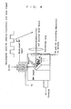
- the reaction chamber used herein is a CVD reaction chamber of which schematic structure is shown in Fig. 1 .
- the reaction chamber 1 comprises a gas introduction port 2 for introduction of reaction gas and dilution gas therefore and a gas exhaust 3 for exhausting the introduced reaction gas and the like to the outside of the chamber and is connected to a vacuum pump so that the inner pressure is maintained at a reduced pressure below the atmospheric pressure.
- a boron nitride deposition substrate 4 is placed on the way of gas flow.
- An optical window 5 is mounted in a part of a wall of the reaction chamber facing the substrate.
- An excimer ultraviolet laser equipment 6 is set in such a manner that the substrate is irradiated with ultraviolet light through the window.
- the reaction gas introduced into the reaction chamber is excited by the ultraviolet light incident on the substrate surface so as to cause gas phase reaction between nitrogen source and boron source in the reaction gas, thereby generating, depositing, or growing a sp3-bonded boron nitride, represented by a general formula BN, having a hexagonal 5H or 6H polytypic form and having a property of emitting light in ultraviolet region.
- a sp3-bonded boron nitride represented by a general formula BN, having a hexagonal 5H or 6H polytypic form and having a property of emitting light in ultraviolet region.
- a plasma torch 7 is provided for this embodiment.
- the reaction gas introduction port and the plasma torch are formed as united part facing the substrate so that the reaction gas and the plasma are directed to the substrate.
- a boron nitride solid material as the boron source.
- Fig. 4 shows the aspect of the reaction in this case. That is, a BN target and a substrate are previously placed in the reaction chamber.
- the disclosed examples show embodiments in which only ammonia gas diluted with Ar gas is introduced as nitrogen source gas as the reaction gas into the reaction chamber through the plasma torch nozzle, embodiments are not limited thereto. That is, it is apparent to a person with ordinary skill in the art that, besides ammonia, gas containing nitrogen or other noble gas can be also used.
- the introduced gas is plasmarized and is directed to the BN target.
- the target is irradiated with exima laser as well as the plasma whereby the target is vaporized its components so as to generate radials of nitrogen and boron or a BN series precursor matter.
- a desired compound i.e. a sp3-bonded boron nitride, represented by a general formula "BN", having a hexagonal 5H or 6H polytypic form and having a property of emitting light in ultraviolet region, is deposited or grown on the substrate.
- the present invention aims to provide a sp3-bonded boron nitride, represented by a general formula "BN", having a hexagonal 5H or 6H polytypic form and a property of emitting light in ultraviolet region, a production method of the same, and applications utilizing the properties of the same, as mentioned above.
- BN sp3-bonded boron nitride
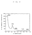
- the X-ray diffraction pattern is shown in Fig. 2 .
- the diffraction results of this pattern are shown in Table 1.
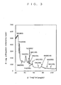
- the X-ray diffraction pattern is shown in Fig. 3 .
- the diffraction results of this pattern are shown in Table 2.
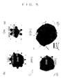
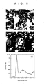
- Fig. 6(b) is an image of cathode luminescence caused by irradiation of electron beam of 20KeV, the cathode luminescence image at 230 nm being taken. It is found that UV emission appears over the entire area of the sample.
- Fig. 6(c) shows a spectrum obtained from the cathode luminescence caused by irradiation of electron beam of 20KeV. It is found that there is sharp luminescence at 225 nm. It is found that there is broad UV emission is present at 300 nm.
- a sp3-bonded hexagonal BN of 5H or 6H type has sharp emission at ultraviolet wavelength of 225 nm which is in a range capable of being used in atmosphere but almost borders on a region of vacuum ultraviolet, the BN has great potential as materials for practical application of solid ultraviolet laser.
- the practical application of solid ultraviolet laser will make immeasurable technical spillover effects on dramatic increase in capacity of rewritable recording media, chemistry, medicine, electronics industry, and others.
Landscapes
- Chemical & Material Sciences (AREA)
- Engineering & Computer Science (AREA)
- Organic Chemistry (AREA)
- Materials Engineering (AREA)
- Chemical Kinetics & Catalysis (AREA)
- Mechanical Engineering (AREA)
- Metallurgy (AREA)
- General Chemical & Material Sciences (AREA)
- Physics & Mathematics (AREA)
- Inorganic Chemistry (AREA)
- Plasma & Fusion (AREA)
- Health & Medical Sciences (AREA)
- Toxicology (AREA)
- Chemical Vapour Deposition (AREA)
- Crystals, And After-Treatments Of Crystals (AREA)
- Luminescent Compositions (AREA)
- Led Devices (AREA)
- Physical Vapour Deposition (AREA)
Claims (17)
- UV-Licht emittierende Vorrichtung, wobei die Vorrichtung eine lichtemittierende Diode oder ein UV-Festkörperlaser ist, wobei die Vorrichtung als ein funktionelles Material sp3-gebundenes Bornitrid aufweist, das durch eine allgemeine Formel BN repräsentiert wird, das eine hexagonale 5H oder 6H polytypische Form und eine Eigenschaft aufweist, Licht im ultravioletten Bereich zu emittieren.
- Vorrichtung nach Anspruch 1, wobei des sp3-gebundene Bornitrid hergestellt wird durch:Einleiten eines Reaktionsmischgases, das Bor und Stickstoff enthält, die mit einem Verdünnungsgas verdünnt sind, in eine Reaktionskammer; und Bestrahlen einer Oberfläche eines in der Kammer angeordneten Substrats, einer Zuchtfläche auf dem Substrat und eines Zuchtabstandsbereichs um die Zuchtfläche mit ultraviolettem Licht, um eine Gasphasenreaktion zu bewirken, wodurch das sp3-gebundene Bornitrid auf dem Substrat erzeugt, abgeschieden oder gezüchtet wird.
- Vorrichtung nach Anspruch 2, wobei das Verdünnungsgas ein Edelgas, Wasserstoff, Stickstoff oder ein Mischgas ist, das aus zwei oder mehreren von diesen besteht, und das Volumenverhältnis des Reaktionsgases zum Verdünnungsgas 100:0,0001-100 beträgt.
- Vorrichtung nach Anspruch 1, wobei des sp3-gebundene Bornitrid hergestellt wird durch:Einführen von Bornitrid als ein Borrohmaterial in eine Reaktionskammer, während in die Reaktionskammer ein Reaktionsmischgas eingeleitet wird, das mit einem Verdünnungsgas verdünnten Stickstoff enthält; Sammeln und Emittieren von ultraviolettem Laserlicht von 190 nm bis 400 nm Wellenlänge auf das feste Bornitridrohmaterial, um es zu verdampfen, um ein Radikal enthaltendes Bor oder eine BN-Vorläufersubstanz zu erzeugen; und Bestrahlen einer Oberfläche eines in der Kammer angeordneten Substrats, einer Zuchtfläche auf dem Substrat und eines Zuchtabstandsbereichs um die Zuchtfläche mit ultraviolettem Licht, um eine Gasphasenreaktion zwischen dem Reaktionsgas, das Stickstoff enthält, und dem ein Radikal enthaltenden Bor oder eine Rekoagulationsreaktion der BN-Vorläufersubstanz im Verdampfungszustand zu bewirken, wodurch das sp3-gebundene Bornitrid auf dem Substrat erzeugt, abgeschieden oder gezüchtet wird.
- Vorrichtung nach Anspruch 1, wobei des sp3-gebundene Bornitrid hergestellt wird durch:Einführen von Bornitrid als ein Borrohmaterial in eine Reaktionskammer, während in die Reaktionskammer ein Reaktionsmischgas eingeleitet wird, das Bor und Stickstoff enthält, die mit einem Verdünnungsgas verdünnt sind; Bestrahlen des festen Bornitridrohmaterials mit Plasma sowie ultraviolettem Laserlicht von 190 nm bis 400 nm Wellenlänge, um es zu verdampfen, um ein Radikal enthaltendes Bor oder eine BN-Vorläufersubstanz zu erzeugen; und Bestrahlen einer Oberfläche eines in der Kammer angeordneten Substrats, einer Zuchtfläche auf dem Substrat und eines Zuchtabstandsbereichs um die Zuchtfläche mit ultraviolettem Licht, um eine Gasphasenreaktion zwischen dem Reaktionsgas, das Stickstoff enthält, und dem ein Radikal enthaltenden Bor oder eine Rekoagulationsreaktion der BN-Vorläufersubstanz im Verdampfungszustand zu bewirken, wodurch das sp3-gebundene Bornitrid auf dem Substrat erzeugt, abgeschieden oder gezüchtet wird.
- Vorrichtung nach Anspruch 4 oder 5, wobei das Verdünnungsgas ein Edelgas, Wasserstoff, Stickstoff oder ein Mischgas ist, das aus zwei oder mehreren von diesen besteht, und das Volumenverhältnis des Reaktionsgases zum Verdünnungsgas 100:0-100 beträgt.
- Vorrichtung nach Anspruch 4 oder 5, wobei der Ultraviolett-Laser ein Impulslaser ist.
- Vorrichtung nach Anspruch 5 oder 7, wobei durch Anwenden eines modulationssynchronisierenden Laserimpulses auf das Plasma das Plasma paketiert wird, um das sp3-gebundene Bornitrid zu erzeugen, abzuscheiden und zu züchten, das eine verbesserte kristalline Eigenschaft aufweist.
- Verwendung eines funktionellen Materials, das sp3-gebundenes Bornitrid enthält, das durch eine allgemeine Formel BN repräsentiert wird, das eine hexagonale 5H oder 6H polytypische Form und eine Eigenschaft aufweist, Licht im ultravioletten Bereich zu emittieren, als Material, das Licht im ultravioletten Bereich emittiert.
- Verwendung nach Anspruch 9, wobei das funktionelle Material hauptsächlich als ein elektronisches Material, insbesondere als lichtemittierende Diode verwendet wird.
- Verwendung nach Anspruch 9 oder 10, wobei des sp3-gebundene Bornitrid hergestellt wird durch:Einleiten eines Reaktionsmischgases, das Bor und Stickstoff enthält, die mit einem Verdünnungsgas verdünnt sind, in eine Reaktionskammer; und Bestrahlen einer Oberfläche eines in der Kammer angeordneten Substrats, einer Zuchtfläche auf dem Substrat und eines Zuchtabstandsbereichs um die Zuchtfläche mit ultraviolettem Licht, um eine Gasphasenreaktion zu bewirken, wodurch das sp3-gebundene Bornitrid auf dem Substrat erzeugt, abgeschieden oder gezüchtet wird.
- Verwendung nach Anspruch 11, wobei das Verdünnungsgas ein Edelgas, Wasserstoff, Stickstoff oder ein Mischgas ist, das aus zwei oder mehreren von diesen besteht, und das Volumenverhältnis des Reaktionsgases zum Verdünnungsgas 100:0,0001-100 beträgt.
- Verwendung nach Anspruch 9 oder 10, wobei des sp3-gebundene Bornitrid hergestellt wird durch:Einführen von Bornitrid als ein Borrohmaterial in eine Reaktionskammer, während ein Reaktionsmischgas eingeleitet wird, das mit einem Verdünnungsgas verdünnten Stickstoff enthält, in die Reaktionskammer; Sammeln und Emittieren von ultraviolettem Laserlicht von 190 nm bis 400 nm Wellenlänge auf das feste Bornitridrohmaterial, um es zu verdampfen, um ein Radikal enthaltendes Bor oder eine BN-Vorläufersubstanz zu erzeugen; und Bestrahlen einer Oberfläche eines in der Kammer angeordneten Substrats, einer Zuchtfläche auf dem Substrat und eines Zuchtabstandsbereichs um die Zuchtfläche mit ultraviolettem Licht, um eine Gasphasenreaktion zwischen dem Reaktionsgas, das Stickstoff enthält, und dem ein Radikal enthaltenden Bor oder eine Rekoagulationsreaktion der BN-Vorläufersubstanz im Verdampfungszustand zu bewirken, wodurch das sp3-gebundene Bornitrid auf dem Substrat erzeugt, abgeschieden oder gezüchtet wird.
- Verwendung nach Anspruch 9 oder 10, wobei des sp3-gebundene Bornitrid hergestellt wird durch:Einführen von Bornitrid als ein Borrohmaterial in eine Reaktionskammer, während in die Reaktionskammer ein Reaktionsmischgas eingeleitet wird, das Bor und Stickstoff enthält, die mit einem Verdünnungsgas verdünnt sind; Bestrahlen des festen Bornitridrohmaterials mit Plasma sowie ultraviolettem Laserlicht von 190 nm bis 400 nm Wellenlänge, um es zu verdampfen, um ein Radikal enthaltendes Bor oder eine BN-Vorläufersubstanz zu erzeugen; und Bestrahlen einer Oberfläche eines in der Kammer angeordneten Substrats, einer Zuchtfläche auf dem Substrat und eines Zuchtabstandsbereichs um die Zuchtfläche mit ultraviolettem Licht, um eine Gasphasenreaktion zwischen dem Reaktionsgas, das Stickstoff enthält, und dem ein Radikal enthaltenden Bor oder eine Rekoagulationsreaktion der BN-Vorläufersubstanz im Verdampfungszustand zu bewirken, wodurch das sp3-gebundene Bornitrid auf dem Substrat erzeugt, abgeschieden oder gezüchtet wird.
- Verwendung nach Anspruch 13 oder 14, wobei das Verdünnungsgas ein Edelgas, Wasserstoff, Stickstoff oder ein Mischgas ist, das aus zwei oder mehreren von diesen besteht, und das Volumenverhältnis des Reaktionsgases zum Verdünnungsgas 100:0-100 beträgt.
- Verwendung nach Anspruch 13 oder 14, wobei der Ultraviolett-Laser ein Impulslaser ist.
- Verwendung nach Anspruch 14 oder 16, wobei durch Anwenden eines modulationssynchronisierenden Laserimpulses auf das Plasma das Plasma paketiert wird, um das sp3-gebundene Bornitrid zu erzeugen, abzuscheiden und zu züchten, das eine verbesserte kristalline Eigenschaft aufweist.
Applications Claiming Priority (3)
| Application Number | Priority Date | Filing Date | Title |
|---|---|---|---|
| JP2002192863 | 2002-07-02 | ||
| JP2002192863A JP3598381B2 (ja) | 2002-07-02 | 2002-07-02 | 一般式;BNで示され、六方晶系5H型ないしは6H型多形構造を有し、紫外域で発光するsp3結合型窒化ホウ素とその製造方法、及びこれを利用した機能性材料 |
| PCT/JP2003/008370 WO2004005186A1 (ja) | 2002-07-02 | 2003-07-01 | 紫外域で発光するsp3結合型窒化ホウ素とその製造方法、及びこれを利用した機能性材料 |
Publications (3)
| Publication Number | Publication Date |
|---|---|
| EP1518824A1 EP1518824A1 (de) | 2005-03-30 |
| EP1518824A4 EP1518824A4 (de) | 2009-06-17 |
| EP1518824B1 true EP1518824B1 (de) | 2012-09-05 |
Family
ID=30112268
Family Applications (1)
| Application Number | Title | Priority Date | Filing Date |
|---|---|---|---|
| EP03738617A Expired - Lifetime EP1518824B1 (de) | 2002-07-02 | 2003-07-01 | IM ULTRAVIOLETTBEREICH LICHT EMITTIRENDES sp3-GEBUNDENES BORNITRID, HERSTELLUNGSVERFAHREN DAFÜR UND FUNKTIONELLES MATERIAL, BEI DEM ES ZUR ANWENDUNG KOMMT |
Country Status (4)
| Country | Link |
|---|---|
| US (1) | US7419572B2 (de) |
| EP (1) | EP1518824B1 (de) |
| JP (1) | JP3598381B2 (de) |
| WO (1) | WO2004005186A1 (de) |
Families Citing this family (21)
| Publication number | Priority date | Publication date | Assignee | Title |
|---|---|---|---|---|
| JP3783057B2 (ja) * | 2003-08-29 | 2006-06-07 | 独立行政法人物質・材料研究機構 | 電界電子放出特性を利する自己造形的表面形状を有するsp3結合性窒化ホウ素薄膜とその製造方法及びその用途 |
| JP2006079873A (ja) * | 2004-09-08 | 2006-03-23 | National Institute For Materials Science | 深紫外線固体発光装置 |
| DE602004031971D1 (de) * | 2003-11-18 | 2011-05-05 | Nat Inst For Materials Science | Einkristall aus hochgereinigtem hexagonalem bornitrid, der zur lichtemission im tiefen ultraviolett mit hoher leuchtdichte befähigt ist, herstellungsverfahren dafür, licht im tiefen ultraviolett mit hoher leuchtdichte emittierende vorrichtung und verofflichtemissionseinheit |
| JP3903185B2 (ja) * | 2004-02-12 | 2007-04-11 | 独立行政法人物質・材料研究機構 | 深紫外線固体発光素子 |
| JP4677629B2 (ja) * | 2004-12-22 | 2011-04-27 | 独立行政法人物質・材料研究機構 | 窒化ホウ素膜表面に先端の尖った結晶が自己相似性フラクタル模様を呈して電子放出に適った密度で二次元分布してなる窒化ホウ素薄膜エミッターとその製造方法 |
| US7715760B2 (en) | 2005-04-19 | 2010-05-11 | Ricoh Company, Ltd. | Charging device, and process cartridge and image forming apparatus using the same |
| JP4859173B2 (ja) * | 2005-07-01 | 2012-01-25 | 独立行政法人物質・材料研究機構 | 遠紫外高輝度発光する高純度六方晶窒化ホウ素単結晶粉末とその製造方法 |
| HU227333B1 (en) * | 2005-09-30 | 2011-03-28 | Univ Szegedi | Method and target-carrier arrangement for building uniform thickness homogeneous coating made of plasm that produced by pulse laser, as well as the coating |
| US7728503B2 (en) | 2006-03-29 | 2010-06-01 | Ricoh Company, Ltd. | Electron emission element, charging device, process cartridge, and image forming apparatus |
| KR100801736B1 (ko) * | 2006-04-06 | 2008-02-11 | 주식회사 하이닉스반도체 | 증가된 센싱마진을 갖는 반도체 메모리소자의 제조방법 |
| JP5170653B2 (ja) * | 2008-03-26 | 2013-03-27 | 独立行政法人物質・材料研究機構 | コーン・エミッタの形成方法 |
| JP5126845B2 (ja) * | 2008-03-26 | 2013-01-23 | 独立行政法人物質・材料研究機構 | 半導体材料とその製造方法 |
| JP5218969B2 (ja) * | 2008-03-26 | 2013-06-26 | 独立行政法人物質・材料研究機構 | sp3−結合性BN高密度相を有するBN薄膜およびその製造方法。 |
| AR075584A1 (es) | 2009-02-27 | 2011-04-20 | Intermune Inc | COMPOSICIONES TERAPEUTICAS QUE COMPRENDEN beta-D-2'-DESOXI-2'-FLUORO-2'-C-METILCITIDINA Y UN DERIVADO DE ACIDO ISOINDOL CARBOXILICO Y SUS USOS. COMPUESTO. |
| JP4822232B2 (ja) * | 2009-03-17 | 2011-11-24 | 独立行政法人物質・材料研究機構 | 六方晶窒化ホウ素単結晶およびそれを用いた紫外線発光素子 |
| US8796151B2 (en) * | 2012-04-04 | 2014-08-05 | Ultratech, Inc. | Systems for and methods of laser-enhanced plasma processing of semiconductor materials |
| JP2014075527A (ja) * | 2012-10-05 | 2014-04-24 | Nippon Telegr & Teleph Corp <Ntt> | 半導体素子構造およびその作製法 |
| WO2016031019A1 (ja) * | 2014-08-28 | 2016-03-03 | 国立大学法人九州大学 | レーザ照射装置及びレーザ照射方法 |
| KR101874225B1 (ko) | 2017-01-04 | 2018-07-03 | 포항공과대학교 산학협력단 | 질화물 반도체 물질의 제조 방법 |
| KR102771621B1 (ko) * | 2019-09-03 | 2025-02-25 | 삼성전자주식회사 | 육방정계 질화붕소의 제조 방법 |
| JP7693118B2 (ja) * | 2023-04-26 | 2025-06-16 | 株式会社トクヤマ | 熱伝導性フィラー、樹脂組成物、樹脂シートおよび六方晶窒化ホウ素粉末の製造方法 |
Family Cites Families (6)
| Publication number | Priority date | Publication date | Assignee | Title |
|---|---|---|---|---|
| US4435445A (en) * | 1982-05-13 | 1984-03-06 | Energy Conversion Devices, Inc. | Photo-assisted CVD |
| JPH0379770A (ja) | 1989-08-19 | 1991-04-04 | Semiconductor Energy Lab Co Ltd | 窒化ホウ素の作製方法 |
| US5080753A (en) * | 1989-12-06 | 1992-01-14 | General Motors Corporation | Laser deposition of crystalline boron nitride films |
| JPH054808A (ja) | 1991-06-24 | 1993-01-14 | Sumitomo Electric Ind Ltd | 窒化硼素膜の製造方法 |
| JPH0733243B2 (ja) | 1992-06-25 | 1995-04-12 | 科学技術庁無機材質研究所長 | 光照射併用プラズマcvd法による硬質窒化ホウ素の製造法 |
| JP2920203B2 (ja) * | 1996-06-25 | 1999-07-19 | 科学技術庁無機材質研究所長 | sp3結合型窒化ホウ素の製造方法 |
-
2002
- 2002-07-02 JP JP2002192863A patent/JP3598381B2/ja not_active Expired - Lifetime
-
2003
- 2003-07-01 US US10/518,644 patent/US7419572B2/en not_active Expired - Fee Related
- 2003-07-01 WO PCT/JP2003/008370 patent/WO2004005186A1/ja not_active Ceased
- 2003-07-01 EP EP03738617A patent/EP1518824B1/de not_active Expired - Lifetime
Also Published As
| Publication number | Publication date |
|---|---|
| JP2004035301A (ja) | 2004-02-05 |
| EP1518824A1 (de) | 2005-03-30 |
| US20060163527A1 (en) | 2006-07-27 |
| US7419572B2 (en) | 2008-09-02 |
| EP1518824A4 (de) | 2009-06-17 |
| JP3598381B2 (ja) | 2004-12-08 |
| WO2004005186A1 (ja) | 2004-01-15 |
Similar Documents
| Publication | Publication Date | Title |
|---|---|---|
| EP1518824B1 (de) | IM ULTRAVIOLETTBEREICH LICHT EMITTIRENDES sp3-GEBUNDENES BORNITRID, HERSTELLUNGSVERFAHREN DAFÜR UND FUNKTIONELLES MATERIAL, BEI DEM ES ZUR ANWENDUNG KOMMT | |
| US5316804A (en) | Process for the synthesis of hard boron nitride | |
| US5403399A (en) | Method and apparatus for vapor deposition of diamond | |
| US5096740A (en) | Production of cubic boron nitride films by laser deposition | |
| US5175020A (en) | Process for depositing a layer containing boron and nitrogen | |
| EP0442490B1 (de) | Verfahren zur Herstellung einer einkristallinen Bornitridschicht | |
| Yi et al. | Luminescence characteristics of ZnGa2O4 thin film phosphors grown by pulsed laser deposition | |
| Ando et al. | Photoenhanced metalorganic chemical vapor deposition of ZnSe films using diethylzinc and dimethylselenide | |
| Okada et al. | Formation of carbon nitride films with high N/C ratio by high‐pressure radio frequency magnetron sputtering | |
| US5606056A (en) | Carbon nitride and its synthesis | |
| Kadono et al. | Diamond deposition from CF4‐H2 mixed gas by microwave plasma | |
| Alexandrescu et al. | Preparation of carbon nitride fine powder by laser induced gas-phase reactions | |
| US5429998A (en) | Crystalline sialon having wurtzite structure | |
| US5286533A (en) | Method of making hard boron nitride by a plasma CVD method employing beam irradiation | |
| EP0406995B1 (de) | Verfahren zur Erzeugung einer Dünnschicht TIN | |
| JP2920203B2 (ja) | sp3結合型窒化ホウ素の製造方法 | |
| JP3783057B2 (ja) | 電界電子放出特性を利する自己造形的表面形状を有するsp3結合性窒化ホウ素薄膜とその製造方法及びその用途 | |
| JPS60245217A (ja) | 薄膜形成装置 | |
| Oumi et al. | Oxygenation Process of Ti–O Films Formed by Reactive Ion Plating | |
| JP2775340B2 (ja) | 合成膜の析出方法 | |
| JP2762910B2 (ja) | 発光材料 | |
| Nayak et al. | Electron beam activated plasma chemical vapour deposition of polycrystalline diamond films | |
| JPH054807A (ja) | 窒化硼素膜の製造方法 | |
| Perea-Lopez et al. | A novel hybrid pulsed laser deposition/metalorganic vapour deposition method to form rare-earth activated GaN | |
| KR20040018009A (ko) | 넓은 에너지 영역에서 띠간격을 갖는 실리콘 카본나이트라이드(SiCN) 박막 제조방법 |
Legal Events
| Date | Code | Title | Description |
|---|---|---|---|
| PUAI | Public reference made under article 153(3) epc to a published international application that has entered the european phase |
Free format text: ORIGINAL CODE: 0009012 |
|
| 17P | Request for examination filed |
Effective date: 20050105 |
|
| AK | Designated contracting states |
Kind code of ref document: A1 Designated state(s): AT BE BG CH CY CZ DE DK EE ES FI FR GB GR HU IE IT LI LU MC NL PT RO SE SI SK TR |
|
| RBV | Designated contracting states (corrected) |
Designated state(s): DE FR GB |
|
| A4 | Supplementary search report drawn up and despatched |
Effective date: 20090520 |
|
| 17Q | First examination report despatched |
Effective date: 20090918 |
|
| GRAP | Despatch of communication of intention to grant a patent |
Free format text: ORIGINAL CODE: EPIDOSNIGR1 |
|
| GRAS | Grant fee paid |
Free format text: ORIGINAL CODE: EPIDOSNIGR3 |
|
| GRAA | (expected) grant |
Free format text: ORIGINAL CODE: 0009210 |
|
| AK | Designated contracting states |
Kind code of ref document: B1 Designated state(s): DE FR GB |
|
| REG | Reference to a national code |
Ref country code: GB Ref legal event code: FG4D |
|
| RIN1 | Information on inventor provided before grant (corrected) |
Inventor name: OKADA, KATSUYUKI, C/O NAT. INST. FOR MATERIALS SCE Inventor name: KOMATSU, SHOJIRO, C/O NAT. INST. FOR MATERIALS SCE Inventor name: MORIYOSHI, YUSUKE, C/O HOSEI UNIVERSITY |
|
| REG | Reference to a national code |
Ref country code: DE Ref legal event code: R096 Ref document number: 60342019 Country of ref document: DE Effective date: 20121031 |
|
| PLBE | No opposition filed within time limit |
Free format text: ORIGINAL CODE: 0009261 |
|
| STAA | Information on the status of an ep patent application or granted ep patent |
Free format text: STATUS: NO OPPOSITION FILED WITHIN TIME LIMIT |
|
| 26N | No opposition filed |
Effective date: 20130606 |
|
| REG | Reference to a national code |
Ref country code: DE Ref legal event code: R097 Ref document number: 60342019 Country of ref document: DE Effective date: 20130606 |
|
| PGFP | Annual fee paid to national office [announced via postgrant information from national office to epo] |
Ref country code: DE Payment date: 20140829 Year of fee payment: 12 |
|
| PGFP | Annual fee paid to national office [announced via postgrant information from national office to epo] |
Ref country code: FR Payment date: 20140717 Year of fee payment: 12 Ref country code: GB Payment date: 20140730 Year of fee payment: 12 |
|
| REG | Reference to a national code |
Ref country code: DE Ref legal event code: R119 Ref document number: 60342019 Country of ref document: DE |
|
| GBPC | Gb: european patent ceased through non-payment of renewal fee |
Effective date: 20150701 |
|
| PG25 | Lapsed in a contracting state [announced via postgrant information from national office to epo] |
Ref country code: DE Free format text: LAPSE BECAUSE OF NON-PAYMENT OF DUE FEES Effective date: 20160202 Ref country code: GB Free format text: LAPSE BECAUSE OF NON-PAYMENT OF DUE FEES Effective date: 20150701 |
|
| REG | Reference to a national code |
Ref country code: FR Ref legal event code: ST Effective date: 20160331 |
|
| PG25 | Lapsed in a contracting state [announced via postgrant information from national office to epo] |
Ref country code: FR Free format text: LAPSE BECAUSE OF NON-PAYMENT OF DUE FEES Effective date: 20150731 |