EP1513098B1 - Procédé et appareil pour une carte à puce de type USB et sans contact - Google Patents
Procédé et appareil pour une carte à puce de type USB et sans contact Download PDFInfo
- Publication number
- EP1513098B1 EP1513098B1 EP04255342A EP04255342A EP1513098B1 EP 1513098 B1 EP1513098 B1 EP 1513098B1 EP 04255342 A EP04255342 A EP 04255342A EP 04255342 A EP04255342 A EP 04255342A EP 1513098 B1 EP1513098 B1 EP 1513098B1
- Authority
- EP
- European Patent Office
- Prior art keywords
- mode
- wireless
- signal
- smart card
- usb
- Prior art date
- Legal status (The legal status is an assumption and is not a legal conclusion. Google has not performed a legal analysis and makes no representation as to the accuracy of the status listed.)
- Expired - Lifetime
Links
Images


Classifications
-
- G—PHYSICS
- G06—COMPUTING OR CALCULATING; COUNTING
- G06K—GRAPHICAL DATA READING; PRESENTATION OF DATA; RECORD CARRIERS; HANDLING RECORD CARRIERS
- G06K19/00—Record carriers for use with machines and with at least a part designed to carry digital markings
- G06K19/06—Record carriers for use with machines and with at least a part designed to carry digital markings characterised by the kind of the digital marking, e.g. shape, nature, code
- G06K19/067—Record carriers with conductive marks, printed circuits or semiconductor circuit elements, e.g. credit or identity cards also with resonating or responding marks without active components
- G06K19/07—Record carriers with conductive marks, printed circuits or semiconductor circuit elements, e.g. credit or identity cards also with resonating or responding marks without active components with integrated circuit chips
- G06K19/077—Constructional details, e.g. mounting of circuits in the carrier
- G06K19/07737—Constructional details, e.g. mounting of circuits in the carrier the record carrier consisting of two or more mechanically separable parts
- G06K19/07739—Constructional details, e.g. mounting of circuits in the carrier the record carrier consisting of two or more mechanically separable parts comprising a first part capable of functioning as a record carrier on its own and a second part being only functional as a form factor changing part, e.g. SIM cards type ID 0001, removably attached to a regular smart card form factor
-
- G—PHYSICS
- G06—COMPUTING OR CALCULATING; COUNTING
- G06K—GRAPHICAL DATA READING; PRESENTATION OF DATA; RECORD CARRIERS; HANDLING RECORD CARRIERS
- G06K19/00—Record carriers for use with machines and with at least a part designed to carry digital markings
- G06K19/06—Record carriers for use with machines and with at least a part designed to carry digital markings characterised by the kind of the digital marking, e.g. shape, nature, code
- G06K19/067—Record carriers with conductive marks, printed circuits or semiconductor circuit elements, e.g. credit or identity cards also with resonating or responding marks without active components
- G06K19/07—Record carriers with conductive marks, printed circuits or semiconductor circuit elements, e.g. credit or identity cards also with resonating or responding marks without active components with integrated circuit chips
- G06K19/077—Constructional details, e.g. mounting of circuits in the carrier
- G06K19/0772—Physical layout of the record carrier
- G06K19/07733—Physical layout of the record carrier the record carrier containing at least one further contact interface not conform ISO-7816
-
- G—PHYSICS
- G06—COMPUTING OR CALCULATING; COUNTING
- G06K—GRAPHICAL DATA READING; PRESENTATION OF DATA; RECORD CARRIERS; HANDLING RECORD CARRIERS
- G06K19/00—Record carriers for use with machines and with at least a part designed to carry digital markings
- G06K19/06—Record carriers for use with machines and with at least a part designed to carry digital markings characterised by the kind of the digital marking, e.g. shape, nature, code
- G06K19/067—Record carriers with conductive marks, printed circuits or semiconductor circuit elements, e.g. credit or identity cards also with resonating or responding marks without active components
- G06K19/07—Record carriers with conductive marks, printed circuits or semiconductor circuit elements, e.g. credit or identity cards also with resonating or responding marks without active components with integrated circuit chips
- G06K19/077—Constructional details, e.g. mounting of circuits in the carrier
- G06K19/07749—Constructional details, e.g. mounting of circuits in the carrier the record carrier being capable of non-contact communication, e.g. constructional details of the antenna of a non-contact smart card
- G06K19/07766—Constructional details, e.g. mounting of circuits in the carrier the record carrier being capable of non-contact communication, e.g. constructional details of the antenna of a non-contact smart card comprising at least a second communication arrangement in addition to a first non-contact communication arrangement
- G06K19/07769—Constructional details, e.g. mounting of circuits in the carrier the record carrier being capable of non-contact communication, e.g. constructional details of the antenna of a non-contact smart card comprising at least a second communication arrangement in addition to a first non-contact communication arrangement the further communication means being a galvanic interface, e.g. hybrid or mixed smart cards having a contact and a non-contact interface
Definitions
- the present disclosure relates generally to smart card (“SC”) devices, and in particular but not exclusively, relates to a smart card device supporting both wireless and wired modes.
- SC smart card
- Smart cards are plastic cards having an embedded integrated circuit ("IC"). That IC may be a logic circuit with its associated memories, a controller with its associated memories and software, or other type of intelligence.
- the IC of an SC is typically coupled to external pads, which allow the SC to communicate or perform transactions with external devices using some type of protocol. These external devices can include an SC reader, a host personal computer (“PC”), SC adapters and connectors, and the like.
- the mechanical and electrical specifications of SCs are published by the International Standard Organization ("ISO") and other organizations.
- the ISO 7816 protocol supports "wired” or “contact modes” for SCs. In the contact mode, the SC physically contacts with the SC reader such that both the SC and SC reader can communicate with each other.
- the ISO 7816 protocol uses a smart card that has external pads including at least a voltage supply pad ("V CC "), a ground pad (“GND”), a reset pad (“RST”), a clock pad (“CLK”), and an input/output pad (“I/O”).
- V CC voltage supply pad
- GND ground pad
- RST reset pad
- CLK clock pad
- I/O input/output pad
- “wireless” or “contact-less” SC standards cover a variety of protocol types such as ISO 10536 (Close-coupled cards), ISO 14443 (Proximity cards), and ISO 15693 (Vicinity cards). Based on these contact-less standards, the contact-less SC and contact-less SC reader communicate with each other without physical connection by placing the SC closely to the SC reader. There is a small loop or antenna inside the contact-less SC, which makes electromagnetic induction contact with the SC reader. After the contact-less SC is placed closely to the contact-less SC reader, the contactless SC will be activated by the electromagnetic field emitted from the SC reader.
- the SC is used with the SC reader connected to the host computer through a USB cable.
- the USB standard has become firmly established and has gained wide acceptance in the PC marketplace.
- the USB standard was developed in response to a need for a standard interface that extends the concept of "plug and play" to devices external to a PC. It has enabled users to install and remove peripheral devices external to the PC without having to open the PC case or to remove power from the PC (e.g., without having to "reboot”).
- the USB standard provides a low-cost, high-performance serial interface that is easy to use and readily expandable, and is supported by an increasing number of SCs that are available in the marketplace.
- the USB cable connected between the USB device and the host computer includes a voltage supply wire ("V BUS "), a ground wire (“GND”), a D-minus wire (“D-”), and a D-plus wire (“D+”).
- a single mode smart card can separately support only one of a contact protocol (e.g., ISO 7816), contact-less protocol (e.g., ISO 14443), or the USB standard protocol. Furthermore, a dual mode smart card has the possibility to switch from an ISO 7816 protocol to a USB protocol or vice versa (such as disclosed in U.S. Patent No. 6,439,464 , assigned to the same assignee as the present application and incorporated by reference herein). The configuration of the smart card is chosen at power-on-reset depending on a hardware mode selection.
- a contact/contact-less dual mode smart card can operate in ISO 7816 mode or in ISO 14443 mode.
- WO99/21119 describes a dual mode data carrier and circuit for such a data carrier.
- the data carrier can be operated in a contact bound mode and in a contact less mode. This document identifies that the contact bound mode and contact less mode may be activated simultaneously. In this case a clock signal detection means inhibits the processing of data to avoid conflicts.
- WO99/34326 teaches a contact/contact less smart card having customizable antenna and interface. On power on the card detects whether the voltage is sufficient for operation. If it is the circuit then detects if the electromagnetic field is on. If the field is on, then the card initializes in a contact less mode, if the field is off, the card initializes in a contact mode.
- WO97/08929 teaches a smart card with a chip, contact field, coils and/or capacitors and a storage element for galvanic or non-galvanic energy and a data exchange with a read and/or write device.
- the device is able to operate with or without contact, the choice of operating the mode can be influenced by additional logic criteria as well as the availability at any given moment of a power supply.
- an apparatus for a smart card comprising: means for receiving a signal sent to the smart card; means for determining whether the signal corresponds to a wired or wireless connection; characterized by: means for automatically switching operation of the smart card between modes in response to the determined connection; and means for operating the smart card in a first mode and for supporting simultaneous operation of the smart card in a second mode, including: means for blocking detection of the second mode if the smart card is operating in the first mode; means for unblocking detection of the second mode after the first mode is stabilized; and means for automatically transitioning from the first mode to the second mode if the signal to the smart card changes.
- the apparatus further comprises means for verifying whether data associated with the first mode is being communicated prior to transitioning to the second mode if no such data is being communicated.
- the apparatus further comprises means for providing a plurality of status signals indicative of mode status of the smart card, and means for polling at least some of these status signals.
- the receiving means comprises an access interface including an antenna and a wired interface
- the determining means comprises a mode detection circuit coupled to the access interface to detect a wireless communication mode and at least one wired communication mode to the smart card; and a switching block coupled to the mode detection circuit to send a set of mode operation signals based on a type of mode detected by the mode detection circuit
- the operating means comprises a controller coupled to the switching block and the mode detection circuit to enable operation of the smart card in a first mode based on the set of mode operation signals, and further to enable change of operation of the smart card to another mode after the first mode.
- the first mode is a wireless or a wired mode.
- the wired mode is a USB mode and the wired interface includes a voltage supply pad, a D- pad, and a D+ pad.
- the mode detection circuit includes: a wireless detection circuit coupled to the antenna to generate a wireless power supply signal and a set of wireless status signals; a power-on detection circuit coupled to the wireless detection circuit and the voltage supply pad to generate a power-on signal and a control signal; a USB detection circuit coupled to the power-on detection circuit, the D+ and the D pads to generate a set of USB status signals including a first USB status signal and a second USB status signal; and a status register coupled to the wireless detection circuit and the USB detection circuit to store the set of wireless status signals and the set of USB status signals.
- the wireless detection circuit includes: a wireless analogue high current unit coupled to the antenna to generate the wireless power supply signal; a wireless analogue low current unit coupled to the antenna and the power-on detection circuit to generate a wireless detection signal; and a first switch responsive to the wireless detection signal to generate the set of wireless status signals.
- the power-on detection circuit includes: a power-on signal generator coupled to the wireless analogue high current unit and the voltage supply pad to generate the power-on signal; and a first logic circuit coupled to the power-on signal generator and the first switch to generate the control signal.
- the USB detection circuit includes: a USB cable detection unit coupled to the first logic circuit, the D+ and the D- pads to generate the first USB status signal; and a second logic circuit coupled to the USB cable detection unit and the controller to generate the second USB status signal.
- the controller includes a processing unit, a wireless macrocell and a wired macrocell, and the switching block is coupled to the wireless macrocell and the wired macrocell to generate the set of mode operation signals to the processing unit.
- the controller is configured to send a wired standby signal to the mode detection circuit and the wireless macrocell is configured to send a wireless ready signal to the switching block if the first mode is the wireless mode and is stable. In other embodiments the controller is configured to send a wireless standby signal to the mode detection circuit and the wired macrocell is configured to send a wired ready signal to the switching block if the first mode is the wired mode and is stable.
- the controller includes a processing unit, a wireless macrocell and a USB macrocell, and wherein the switching block is coupled to a CLK pad, a RST pad, an I/O pad, a wireless macrocell, and a USB macrocell to generate the set of mode operation signals to the processing unit.
- the determining means comprises: a first detection circuit to detect a wireless connection to the smart card; a second detection circuit to detect a wired connection to the smart card; and a switching block coupled to the first and second detection circuits to generate a first signal that corresponds to a type of connection detected by one of the detection circuits; and the operating means comprises a controller coupled to the switching block and responsive to the first signal to allow operation of the smart card in a first mode that corresponds to the type of detected connection, and to allow the smart card to support a second mode that corresponds to a second signal provided by the switching block and to automatically transition operation of the smart card to the second mode in response to the second signal.
- the wired connection comprises at least one of a USB-compliant connection and an ISO-compliant contact connection.
- the wireless or wired connections each comprise a plurality of different types of protocol connections that are supported by the smart card.
- a method for a smart card comprising: receiving a signal sent to the smart card; determining whether the signal corresponds to a wired or a wireless connection; characterized by: automatically switching operation of the smart card between modes in response to the determined connection; operating the smart card in a first mode and for supporting simultaneous operation of the smart card in a second mode, including ; blocking detection of a second mode if the smart card is operating in the first mode; unblocking detection of the second mode after the first mode is stabilized; automatically transitioning operation of the smart card from the first mode to the second mode if the signal to the smart card changes.
- the first mode is a wireless mode and the operating the smart card in the first mode comprises: blocking a wired detection if the wireless signal is detected during the power-on process; and configuring the smart card into the wireless mode and launching a vector-reset process.
- operating the smart card in the first mode further comprises: enabling the wired detection if the smart card is stable in the wireless mode; activating the wired mode if the wired connection is detected.
- the first mode is a wired mode and the operating the smart card in the first mode comprises: blocking a wireless detection, configuring the smart card into the wired mode and launching a vector-reset process for the smart card if the wireless signal is not detected during the power-on process; and activating the wired mode if the wired connection is detected after the end of the power-on process.
- operating the smart card in the first mode further comprises: enabling the wireless detection if the smart card is stable in the wired mode; activating a wireless interface if the wireless signal is detected and if a USB mode operation signal is not sent.
- an embodiment of the invention provides a smart card apparatus to support a wireless mode or a wired mode, such as a USB mode, without conflict. Furthermore, this apparatus can operate in both the wireless mode and wired mode without switching power off and on to change configuration. According to the embodiment of the present invention, the smart card apparatus could decide which mode it shall select and avoid any conflicts between two modes.
- the contact-less or wireless mode can be detected by placing the smart card apparatus close to the contact-less smart card reader, and the USB mode can be detected by the introduction of the smart card apparatus in a USB plug.
- the apparatus will first detect if there is a contact-less mode during a power-on-reset process, and if not then, the apparatus further detects if there is a USB mode after the power-on-reset process. After one mode is detected, the apparatus blocks the other mode detection to avoid conflict. However, after the apparatus is stabilized in the detected mode, the apparatus could further release the blocked mode such that the apparatus could subsequently detect and operate in one or both modes as needed.
- a smart card apparatus that supports a wireless mode, a USB mode or other contact mode without conflict.
- This embodiment of the smart card apparatus can operate in both the wireless and wired modes without switching power off and on to change configuration.
- the wireless mode can be detected by placing the smart card apparatus close to the contact-less smart card reader, and the USB mode can be detected by the introduction of the smart card apparatus in a USB plug.
- the contact mode can be detected by the introduction of the smart card in an ISO 7816 smart card reader, which provides power supply, I/O, CLK and RST signals, or in other type of contact-mode reader.
- the smart card detects the USB mode at power-on reset, and blocks the RF detector.
- the embedded software confirms the USB mode detection, and initializes the smart card with its USB configuration and enables the RF detector again.
- a control signal disabled the RF detector and signals generator.
- the embedded software completed the USB configuration, it enabled the RF detector and signals generator by setting a register bit. In other words, there is a hardware lock of the detection, and there is a software unlock of the detection in an embodiment.
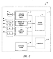
- an embodiment of a smart card apparatus 10 of the present invention could be embedded in a smart card 100 with a plastic body 200.
- the apparatus 10 operates in one of a wireless mode and a wired mode, such as a USB mode, without any conflict during operation.
- the apparatus 10 could operate in both the wireless mode and the USB mode without switching power off and on to change configuration.
- the smart card 100 could be activated by a smart card reader 300 by physically contacting the smart card 100 to the smart card reader 300 or by placing the smart card 100 closely to the smart card reader 300, depending on the protocol supported by the smart card reader 300.
- the apparatus 10 of an embodiment of the present invention could also be implemented in a subscriber identity module (SIM) card for mobile phone or in other devices.
- SIM subscriber identity module
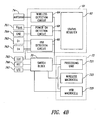
- an embodiment of the apparatus 10 includes a mode detection circuit 11, a switching block 20, a controller 22, an antenna 24, and a wired interface 26 comprising a plurality of electrical pads.
- the antenna 24 could receive wireless signals from and transmit response signals to a contact-less smart card reader.
- the wired interface 26 in one embodiment includes a voltage supply ("V BUS ”) pad 261, a ground (“GND”) pad 264, a D-minus (“D-”) pad 262, and a D-plus (“D+”) pad 263. These pads are in compliance with the USB protocol such that a USB host could access the apparatus 10 through these pads, in one embodiment.
- the mode detection circuit 11, connected to the antenna 24 and the wired interface 26, could detect and store a set of wireless status signals and a set of USB status signals.
- the controller 22 and the switching block 20, connected to each other, could operate the apparatus 10 in the wireless mode or the USB mode (while being able to detect a need to transition to the other mode), based on the set of wireless status signals and the set of USB status signals.
- the mode detection circuit 11 includes a status register 12, a wireless detection circuit 14, a USB detection circuit 16, and a power-on detection circuit 18.
- the wireless detection circuit 14 coupled to the antenna 24 generates a wireless power supply signal to the power-on detection circuit 18 and the set of wireless status signals to the status register 12.
- the power-on detection circuit 18 connected to the wireless detection circuit 14 and the voltage supply pad 261 can generate a power-on signal.
- the wireless detection circuit 14 will receive the electromagnetic power and generate the wireless power supply signal to the power-on detection circuit 18. Then, the power-on detection circuit 18 will generate the power-on signal.
- This power-on signal will also be generated when there is electric power sent through the voltage supply pad 261 to the power-on detection circuit 18 during a wired connection.
- the USB detection circuit 16 coupled to the power-on detection circuit 18, the D+ pad 263, and the D-minus pad 262 generates the set of USB status signals.
- the status register 12 couples to the wireless detection circuit 14 and the USB detection circuit 16 to store the set of wireless status signals and the set of USB status signals, respectively.
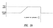
- the apparatus 10 decides which mode it shall select and avoids any conflicts between two modes. To avoid such conflict, the apparatus 10 will first detect if there is a wireless mode, and if not, then the apparatus 10 further detects if there is a USB mode or other wired mode. When the smart card 100 is placed closely to the contact-less smart card reader or connected to a USB host, the apparatus 10 will receive electric power from the contact-less smart card reader or from the USB host, and the power-on signal will be generated by the power-on detection circuit 18, as mentioned above. If the mode detection circuit 11 detects a wireless signal through the antenna 24 when the power-on signal is set to a first state, such as "1," the apparatus 10 will operate in the wireless mode.
- the apparatus 10 will operate in the USB mode.
- the USB cable connection can be decided through at least one of the D+ pad 263 and the D- pad 262 when the USB cable is connected to the USB host.
- the period before the power-on signal goes from the first state to the second state could be defined as a power-on process. That is, the wireless signal will be detected during the predetermined power-on process and the USB cable connection will be detected after the power-on process in an example embodiment.
- the second mode detection such as the USB mode detection
- the wireless detection circuit 14 could be blocked by one of the set of USB status signals
- the USB detection circuit 16 could be blocked by one of the set of wireless status signals.
- the mode detection circuit 11 first detects the wireless mode, then the USB detection circuit 16 is blocked and the apparatus 10 will be configured and be set or reset into the wireless mode. After the apparatus 10 stabilizes in the wireless mode, the mode detection circuit 11 could then enable the USB detection circuit 16 again so that if the smart card 100 is placed in a wired environment, the apparatus 10 can automatically detect the wired environment and transition to that operating mode.
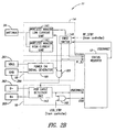
- Fig. 2B is a more detailed schematic diagram of an embodiment of the mode detection circuit 11 of Fig. 2 .
- the wireless detection circuit 14 comprises a wireless analog high current unit 143, a wireless analog low current unit 141, and a first switch 145.
- the wireless analog high current unit 143 couples to the antenna 24 to generate the wireless power supply signal to the power-on detection circuit 18. That is, when the smart card 100 is placed closely to the contact-less smart card reader, the wireless analog high current unit 143 will generate the wireless power supply signal to the power-on detection circuit 18.
- the wireless analog low current unit 141 coupled to the antenna 24 and the power-on detection circuit 18 generates a wireless detection signal to the first switch 145.
- the first switch 145 coupled to the wireless analog low current unit 141 generates the set of wireless status signals including a first wireless status signal (hereinafter “RF_DET signal”) if a wireless signal was detected and a second wireless status signal (hereinafter “CTLESS2 signal”) in another situation to indicate that the wireless interface is enabled while the smart card 100 is in USB mode.
- RF_DET signal a first wireless status signal
- CLESS2 signal a second wireless status signal
- the RF_DET signal When a wireless signal is detected during the power-on process, the RF_DET signal is set to "1." In this case, the RF_DET signal is provided to the status register 12 by way of the first switch 145 to indicate that the wireless mode is detected. Thereafter, a CTLESS bit in the status register 12 is set to "1," the apparatus 10 will be configured in the wireless mode, the USB detection circuit 16 will be blocked by the RF_DET signal, and then the apparatus 10 launches a vector-reset process to initiate the state of the apparatus 10.
- the power-on detection circuit 18 includes a power-on signal generator 181 and a first logic circuit 183.
- the power-on signal generator 181 coupled to the wireless analog high current unit 143, could receive the wireless power supply signal and generate the power-on signal.
- the power-on signal generator 181 also couples to the voltage supply pad 261 and generates the power-on signal when it receives the electric power from the voltage supply pad 261 instead of the antenna 24.
- the power-on signal will be sent to the wireless analog low current unit 141 and the first logic circuit 183, such that the wireless signal will be detected during the predetermined power-on process and the USB cable connection will be detected after the power-on process, as explained above.
- the first logic circuit 183 coupled to the power-on signal generator 181 and the first switch 145, generates a control signal to the USB detection circuit 16.
- the USB detection circuit 16 detects the USB cable connection when the USB detection circuit 16 is not blocked by RF_DET signal and after the power-on signal goes from "1" to "0.”
- the control signal will control the USB detection circuit 16 such that it operates only after the predetermined power-on process and when USB mode detection is not blocked. Therefore, the first logic circuit 183 generates the control signal based on the content of the RF_DET signal and the power-on signal.
- the USB detection circuit 16 includes a USB cable detection unit 163 and a second logic circuit 165 to generate the set of USB status signals including a first USB status signal and a second USB status signal.
- the USB cable detection unit 163 coupled to the power-on detection circuit 18, the D- pad 262 and the D+ pad 263, generates the first USB status signal (hereinafter "USBCONNECT signal").
- USBCONNECT signal When a USB cable connection is detected from at least one of the D+ pad and the D- pad after the end of the power-on process, the USBCONNECT signal is set to "1.”
- the second logic circuit 165 coupled to the USB cable detection unit 163 and the controller 22, generates the second USB status signal (hereinafter "USB2 signal") if the USB interface is enabled while the smart card 100 is in the wireless mode.
- USB2 signal The functions of the USB_STBY signal and the RF_STBY signal which are shown in Fig. 2B will be explained later.
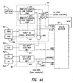
- Fig. 2C is a more detailed schematic diagram of an embodiment of the controller 22 and the switching block 20.
- the controller 22 comprises a processing unit 221, a wireless macrocell 223, and a wired or USB macrocell 225.
- the switching block 20 couples to the wireless macrocell 223 and the wired macrocell 225.
- the wireless macrocell 223 sends a set of wireless mode operation signals including CTLESS_RST, CTLESS_CLK, and CTLESS_I/O signals to the switching block 20.
- the set of the wireless mode operation signals is decoded by the wireless analog low current unit 141 from the wireless signals received by the antenna 24, and which are provided by the wireless analog low current unit 141 to the wireless macrocell 223.
- the wired macrocell 225 generates a set of USB mode operation signals including USB_RST and USB_CLK signals to the switching block 20.
- the second mode detection will be blocked.
- the second mode detection could be enabled again. If the mode detection circuit 11 first detects the wireless mode and sets the RF_DET signal to "1," the USB detection circuit 16 is blocked by such RF_DET signal and the apparatus 10 will be configured and be reset into the wireless mode. After the apparatus 10 stabilizes in the wireless mode, the mode detection circuit 11 could then enable the USB detection circuit 16 again.
- the controller 22 will send a wired standby signal ("USB_STBY”) signal to the USB detection circuit 16 showing that the wired macrocell 225 is placed in a stand-by status during the wireless mode.
- USB_STBY wired standby signal
- second logic circuit 165 sets the USB2 signal to "1" showing that the USB interface (e.g., the wired macrocell 225, the D+ pad 263, and the D- pad 262) is enabled during the wireless mode.
- a wireless ready (“RFREADY”) signal is also sent from the wireless macrocell 223 to the switching block 20 indicating that there is no conflict to activate the USB interface in wireless mode, prior to switching the switching block 20.
- the mode detection circuit 11 first detects the USB cable connection and the USBCONNECT signal is set to "1," the wireless detection circuit 14 is blocked by such USBCONNECT signal and the apparatus 10 will be configured and be set or reset into the USB mode. After the apparatus 10 stabilizes in the USB mode, the mode detection circuit 11 could then enable the wireless detection circuit 14 again.
- the controller 20 will send a wireless standby ("RF_STBY") signal to the wireless detection circuit 14 showing that the wireless macrocell 223 is placed in a stand-by status during the USB mode. If at that time a wireless signal is detected by the wireless detection circuit 14, then the first switch 145 sets the CTLESS2 signal to "1" showing that the contact-less interface (e.g.
- the wireless communication path between the antenna 24 and the wireless macrocell 225) is enabled during the USB mode.
- a wired ready (“USBREADY”) signal is also sent from the wired macrocell 225 to the switching block 20 indicating that there is no conflict to activate the contactless interface in USB mode, prior to switching the switching block 20.
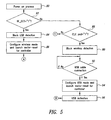
- FIG. 3 A method according to an embodiment of the present invention will now be discussed while referring to Fig. 3 .
- This method operates the apparatus 10 in one of a wireless mode and a USB mode (or other wired mode) without any conflict during operation. Furthermore, this method could operate the apparatus in both the wireless and USB mode without switching power off and on to change configuration.
- the apparatus 10 includes the wired interface 26 having a D- pad 262, and a D+ pad 263.
- the apparatus 10 also includes the switching block 20 and the controller 22 including the wireless macrocell 223 and the wired or USB macrocell 225.
- the method begins (block 30) on a power-on process.
- This power-on process begins when the apparatus 10 is placed closely to the contact-less smart card reader or connected to a USB host.
- the method decides whether a wireless signal is detected during the power-on process. If the wireless signal is detected the method will operate in the wireless mode.
- the method blocks the USB mode detection (at block 34), configures the apparatus 10 in wireless mode and launches a vector-reset process for the controller (block 36).
- Configuring the apparatus 10 in the wireless mode includes configuring the switching block 20 and configuring the wireless macrocell 223 such that the apparatus 10 could operates in the wireless mode.
- the method then blocks the wireless mode detection (block 38). However, in this case when the wireless signal is not detected, the method next decides whether a USB cable connection is detected after the power-on process (block 40).
- the USB cable connection could be detected from at least one of the D+ pad 262 and the D- pad 263 after the end of the power-on process.
- the method then configures the apparatus 10 in USB mode (if the USB cable connection is detected) and launches vector-reset process for the controller (block 42).
- Configuring the apparatus 10 in the USB mode includes configuring the switching block 20 and configuring the wired or USB macrocell 225 such that the apparatus 10 could operate in the USB mode.
- the switching block 20 is configured first, followed by USB cable detection, and then configuration of the USB macrocell 225. If the USB cable connection is detected and after configuration at block 42, then the method will operate a USB activation (block 44) including the USB attachment and the USB initialization.
- the method could enable the USB mode detection (block 46). To enable the USB mode detection, the method will place the wired or USB macrocell 225 in stand-by status and enable the USB cable detection unit 163. After the USB mode detection is enabled, the method then detects whether there is a USB cable connection (block 48).
- USB activation process block 50.
- USB and wired One of these modes is used at any one time to communicate with a host, via use of the USBREADY and RFREADY signals to verify that there is no current data transfer and/or other potential sources of conflict.
- the method could enable the wireless mode detection (block 52). To enable the wireless mode detection, the method will place the wireless macrocell 223 in stand-by status and enable the output of the wireless detection circuit 14. After the wireless mode detection is enabled, the method then decides whether a wireless signal is detected (block 54). If at that time the wireless signal is detected, then the method further decides whether the wired or USB macrocell 225 is still sending the USB_CLK signal to the switching block 20 (block 56), as one embodiment switches from the USB_CLK to another oscillator before switching the switching block 20 to wireless mode. If the USB_CLK signal is no longer being used, the method will then start the contact-less interface (block 58) to allow wireless communication.
- the apparatus 60 operates in one of a wireless mode, a USB mode, and some other contact mode without any conflict during operation. Furthermore, the apparatus 60 could operate in either or both the wireless mode and USB mode without switching power off and on to change configuration.
- the apparatus 60 also includes a mode detection circuit 61, a switching block 70, a controller 72, an antenna 74, and a wired interface 76 comprising a plurality of pads.
- the antenna 74 could receive electromagnetic power and wireless signals from a contact-less smart card reader.
- the wired interface 76 in the embodiment includes a voltage supply pad 761, a ground pad 764, a D- pad 762 and a D+ pad 763, and a set of contact pads including a CLK pad 765, a RST pad 766, and an I/O pad 767 (or other type of contact pads).
- the set of the contact pads are in compliance with the ISO 7816 protocol, as one example, such that an ISO 7816 smart card reader could access the apparatus 60 through the set of contact pads.
- the mode detection circuit 61 connected to the antenna 74 and the wired interface 76, could detect and store a set of wireless status signals and a set of USB status signals.
- the controller 72 and the switching block 70 connected to each other, could operate the apparatus 60 in one of the wireless mode, the USB mode and the contact mode, or operate the apparatus 60 in both the wireless mode and the USB mode, based on the set of wireless status signals and the set of USB status signals.
- the mode detection circuit 61 comprises a status register 62, a wireless detection circuit 64, a USB detection circuit 66, and a power-on detection circuit 68.
- the wireless detection circuit 64 coupled to the antenna 74, generates a wireless power supply signal to the power-on detection circuit 68 and the set of wireless status signals to the status register 62.
- the power-on detection circuit 68 connected to the wireless detection circuit 64 and the voltage supply pad 761 can generate a power-on signal.
- the wireless detection circuit 64 will receive the electromagnetic power and generate the wireless power supply signal to the power-on detection circuit 68. Then, the power-on detection circuit 68 will generate the power-on signal.
- this power-on signal will also be generated when there is electric power sent through the voltage supply pad 761 to the power-on detection circuit 68.
- the USB detection circuit 66 coupled to the power-on detection circuit 68, the D+ pad 763, the D- pad 762 and the CLK pad 765, generates a set of USB status signals and a mode status signal.
- the status register 62 coupled to the wireless detection circuit 64 and the USB detection circuit 66 stores the set of wireless status signals, the set of USB status signals, and the mode status signal.
- the apparatus 60 will first detect if there is a wireless mode, and if not, then the apparatus 60 further detects if there is a USB mode or a contact mode. During the power-on process, if the mode detection circuit 61 detects a wireless signal through the antenna 74, the apparatus 60 will operate in the wireless mode. On the other hand, if the wireless signal is not detected by the mode detection circuit 61 during the power-on process, the apparatus 60 then has to decide whether it is in the USB mode or the contact mode. After the end of the power-on process, the mode detection circuit 61 will further check the CLK pad 765.
- the apparatus 60 will operate in the USB mode. In case that the CLK pad 765 is not set to "1" and the RST pad 766 is set to "1" after the power-on process, the apparatus 60 will operate in the contact mode. It is appreciated that other pad(s) may be checked to detect USB connections or other type of wired connection.
- Fig. 4A is a detailed schematic diagram of an embodiment of the mode detection circuit 61.
- the wireless detection circuit 64 comprises a wireless analog high current unit 643, a wireless analog low current unit 641, and a first switch 645.
- the wireless analog high current unit 643 coupled to the antenna 74 generates the wireless power supply signal to the power-on detection circuit 68. That is, when the smart card is placed closely to the contact-less smart card reader, the wireless analog high current unit 643 will generate the wireless power supply signal to the power-on detection circuit 68.
- the wireless analog low current unit 641 coupled to the antenna 74 and the power-on detection circuit 68 generates a wireless detection signal to the first switch 645.
- the first switch 645 coupled to the wireless analog low current unit 641 generates the set of wireless status signals including a RF_DET signal if a wireless signal was detected, and a CTLESS2 signal in another situation to indicate that the wireless interface is enabled while the smart card is in USB or other contact mode.
- the RF_DET status signal is set to "1.”
- the RF_DET signal is provided to the status register 62 via the first switch 645 to indicate that the wireless mode is detected.
- a CTLESS bit in the status register 62 is set to "1," the apparatus 60 will be configured in the wireless mode, the USB detection circuit 66 will be blocked when RF_DET signal is set to "1,” and then the apparatus 60 launches a vector-reset process to initiate the state of the apparatus 60.
- the power-on detection circuit 68 comprises a power-on signal generator 681 and a first logic circuit 683.
- the power-on signal generator 681 coupled to the wireless analog high current unit 643, could receive the wireless power supply signal and generate the power-on signal. Furthermore, the power-on signal generator 681 also couples to the voltage supply pad 761 and generates the power-on signal when it receives the electric power from the voltage supply pad 761 instead of the antenna 74.
- the first logic circuit 683 coupled to the power-on signal generator 681 and the first switch 645, generates a control signal to the USB detection circuit 66.
- the first logic circuit 683 generates the control signal based on the content of the RF_DET signal and the power-on signal. The control signal will control or block the USB mode and contact mode detection such that both modes could only be detected after the power-on process and when the RF_DET signal is not set to "1.”
- the USB detection circuit 66 includes a USB mode detection unit 661, a USB cable detection unit 663 and a second logic circuit 665 to generate the set of USB status signals including a first USB status signal ("USBCONNECT") and a second USB status signal (“USB2”), and to generate a mode status signal (“MODE”).
- the USB cable detection unit 663 coupled to the D- pad 762 and the D+ pad 763 generates the USBCONNECT signal.
- the USBCONNECT signal is set to "1.” If the MODE signal is set to "1" and the USBCONNECT signal is also set to "1", then the apparatus 60 will operate in the USB mode.
- the apparatus 60 will operate in the contact mode.
- the contact connection could be detected if there is a reset signal detected from the RST pad 766. This contact mode could be the default mode in the apparatus 60.
- the second logic circuit 665 couples to the USB cable detection unit 663 and the controller 70 to generate the USB2 signal.
- Fig. 4B is a more detailed schematic diagram of the controller 72 and the switching block 70 according to an embodiment.
- the controller 72 comprises a processing unit 721, a wireless macrocell 723, and a USB macrocell 725.
- the switching block 70 couples to the wireless macrocell 723, the USB macrocell 725, and the set of contact pads including the CLK pad 765, the RST pad 766, and the I/O pad 767.
- the wireless macrocell 723 generates a set of wireless mode operation signals including CTLESS_RST, CTLESS_CLK, and CTLESS_I/O signals to the switching block 70.
- the USB macrocell 725 generates a set of USB mode operation signals including USB_RST and USB_CLK signals to the switching block 70.
- the set of the contact pads will receive a set of contact mode operation signals including a CT_RST signal, a CT_CLK signal and a CT_I/O signal from the ISO 7816 or other smart card reader to the switching block 70. If the RF_DET signal is set to "1,” then the switching block 70 transmits the set of wireless mode operation signals to the processing unit 721. On the other hand, if the RF_DET signal is set to "0" and the MODE signal is set to "1”, then the switching block 70 transmits the set of USB mode operation signals to the processing unit 721. Furthermore, if the RF_DET signal is set to "0" and the MODE signal is not set to "1”, then the switching block 70 transmits the set of contact mode operation signals to the processing unit 721.
- the other mode detection will be blocked. Furthermore, there is an option to block the other mode detection until a new power-on-reset of the apparatus 60, or to block the other mode detection during the time to stabilize the apparatus 60 in the first mode and thereafter to release the block to enable the other mode detection if needed.
- the second mode detection could be enabled again. For example, if the mode detection circuit 61 first detects the wireless mode and sets the RF_DET signal to "1," the USB detection and the contact mode detection are blocked by this RF_DET signal and then the apparatus 60 will be configured and be reset into the wireless mode.
- USB_STBY USB standby
- second logic circuit 165 sets the USB2 signal to "1" showing that the USB interface is enabled in wireless mode.
- RFREADY wireless ready
- the mode detection circuit 61 first sets the MODE signal to "1,” the wireless detection circuit 64 is blocked by this MODE signal. If the MODE signal is set to "1" and the USBCONNECT signal is also set to “1” then the apparatus 60 will be configured and be reset into the USB mode. After the apparatus 60 stabilizes in the USB mode, the apparatus 60 could then enable the wireless detection circuit 14 again. The controller 72 will then send a wireless standby (“RF_STBY”) signal to the wireless detection circuit 64 showing that the wireless macrocell 723 is placed in a stand-by status even in the USB mode.
- RF_STBY wireless standby
- USB ready (USBREADY) signal is also sent from the USB macrocell 725 to the switching block 70, after verifying that there is no wired data currently being communicated and before switching the switching block 70, so as to indicate that there is no conflict to activate the contact-less interface in USB mode.
- This method operates the apparatus 60 in one of a wireless mode, a USB mode, and a contact mode without any conflict during operation. Furthermore, this method could operate the apparatus in both the wireless and wired modes without switching power off and on to change configuration.
- the apparatus 60 includes the wired interface 76 including a D- pad 762, a D+ pad 763, a CLK pad 765 and a RST pad 766.
- the apparatus 60 also includes the switching block 70 and the controller 72, including the wireless macrocell 723 and the USB macrocell 725.
- the method begins on a power-on process (block 80).
- This power-on process begins when the apparatus 60 is placed closely to the contact-less smart card reader, connected to a USB host, or connected to the contact smart card reader.
- the method decides whether a wireless signal is detected during the power-on process. If the wireless signal is detected the method will operate in the wireless mode.
- the method blocks the USB mode detection (at block 84), configures the apparatus 60 in wireless mode and launches vector-reset process for the controller (block 86).
- the method further determines whether the signal on the CLK pad 765 is set to "1" (at block 88) after the end of the power-on process. If the signal on the CLK pad is set to "1,” then the method blocks the wireless mode detection (at block 90), and decides whether a USB cable connection is detected (block 94).
- the method configures the apparatus 60 in USB mode and launches a vector-reset process for the controller (block 94), and will operate the USB activation (block 96), with the mode signal being set to "1.”
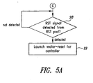
- the method will decide whether there is a contact connection detected.
- the contact connection could be detected if there is a reset signal detected from the RST pad 766 for example in an embodiment, as shown in block 98 of Fig. 5A .
- the mode signal may be set to "0" while RF_DET is "0,” to indicate the possibility of some contact connection. If there is a reset signal detected, then the method will launch a vector-reset process for the controller (block 99) and the apparatus 60 then operates in the contact mode.
- the apparatus 60 could operate in both wireless mode and the USB mode without switching power off and on to change configuration.
- the method could enable the USB mode detection (block 46, shown in Fig. 3A ). To enable the USB mode detection, the method will place the USB macrocell 625 in stand-by status. The method then detects whether there is a USB cable connection, and if the USB cable connection is detected and there is no conflict per the RFREADY signal, then the method will operate the USB activation (block 50, shown in Fig. 3A ).
- the method could enable the wireless mode detection (block 52, shown in Fig. 3B ). To enable the wireless mode detection, the method will place the wireless macrocell 623 in stand-by status. After the wireless mode detection is enabled, the method then decides whether a wireless signal is detected (block 54, shown in Fig. 3B ). If at that time the wireless signal is detected and there is no conflict per the USBREADY signal, then the method further decides whether the USB macrocell 625 still sends the USB_CLK signal to the switching block 60 (block 56, shown in Fig. 3B ). If there is no the USB_CLK signal still being sent from the USB macrocell 625 to the switching block 60, the method will then start the contact-less interface.
Landscapes
- Engineering & Computer Science (AREA)
- Computer Hardware Design (AREA)
- Microelectronics & Electronic Packaging (AREA)
- Physics & Mathematics (AREA)
- General Physics & Mathematics (AREA)
- Theoretical Computer Science (AREA)
- Power Sources (AREA)
Claims (22)
- Appareil pour carte à puce, l'appareil comprenant :un moyen (24, 26) pour recevoir un signal envoyé à la carte à puce ;un moyen (11) pour déterminer si le signal correspond à une connexion filaire ou à une connexion sans fil ;caractérisé par :un moyen (11) pour commuter automatiquement l'exploitation de la carte à puce entre des modes en réponse à la connexion déterminée ; etun moyen (22) pour exploiter la carte à puce dans un premier mode et pour supporter l'exploitation simultanée de la carte à puce dans un second mode, comportant :un moyen pour bloquer la détection du second mode si la carte à puce fonctionne dans le premier mode ;un moyen pour débloquer la détection du second mode après stabilisation du premier mode ; etun moyen pour passer automatiquement du premier mode au second mode si le signal allant à la carte à puce change, et après avoir détecté que le second mode a été débloqué.
- Appareil selon la revendication 1, comprenant en outre un moyen pour vérifier si des données associées au premier mode sont communiquées ou non avant le passage au second mode si aucune telle donnée n'est communiquée.
- Appareil selon la revendication 1 ou 2, comprenant en outre un moyen pour fournir une pluralité de signaux d'état indicatifs d'un état de mode de la carte à puce, et un moyen pour interroger au moins certains de ces signaux d'état.
- Appareil selon l'une quelconque des revendications précédentes, dans lequel :le moyen de réception comprend une interface d'accès comprenant une antenne (24) et une interface filaire (26) ;le moyen de détermination comprend un circuit de détection de mode (11) couplé à l'interface d'accès pour détecter un mode de communication sans fil et au moins un mode de communication filaire avec la carte à puce ; et un bloc de commutation (20) couplé au circuit de détection de mode pour envoyer un ensemble de signaux d'activation de mode en fonction d'un type de mode détecté par le circuit de détection de mode ; etle mode d'exploitation comprend un contrôleur (22) couplé au bloc de commutation et au circuit de détection de mode (11) pour valider l'exploitation de la carte à puce dans un premier mode en fonction de l'ensemble de signaux d'activation de mode, et en outre pour valider le changement d'exploitation de la carte à puce sur un autre mode après le premier mode.
- Appareil selon la revendication 4, dans lequel le premier mode est un mode sans fil ou un mode filaire.
- Appareil selon la revendication 4 ou 5, dans lequel le mode filaire est un mode USB et l'interface filaire comporte une plage d'alimentation de tension (261), une plage D- (262), et une plage D+ (263).
- Appareil selon l'une quelconque des revendications 4 à 6, dans lequel le circuit de détection de mode (11) comporte :un circuit de détection sans fil (14) couplé à l'antenne pour générer un signal d'alimentation électrique sans fil et un ensemble de signaux d'état sans fil ;un circuit de détection de mise sous tension (18) couplé au circuit de détection sans fil et à la plage d'alimentation de tension pour générer un signal de mise sous tension et un signal de commande ;un circuit de détection USB (16) couplé au circuit de détection de mise sous tension, aux plages D+ et D afin de générer un ensemble de signaux d'état USB comportant un premier signal d'état USB et un second signal d'état USB ; etun registre d'état (12) couplé au circuit de détection sans fil et au circuit de détection USB pour stocker l'ensemble de signaux d'état sans fil et l'ensemble de signaux d'état USB.
- Appareil selon la revendication 7, dans lequel le circuit de détection sans fil (14) comporte :une unité analogique sans fil à courant élevé (143) couplée à l'antenne (24) pour générer le signal d'alimentation électrique sans fil ;une unité analogique sans fil à faible courant (141) couplée à l'antenne (24) et au circuit de détection de mise sous tension (18) pour générer un signal de détection sans fil ; etun premier commutateur (145) sensible au signal de détection sans fil pour générer l'ensemble de signaux d'état sans fil.
- Appareil selon la revendication 7 ou 8, dans lequel le circuit de détection de mise sous tension (18) comporte :un générateur de signal de mise sous tension (181) couplé à l'unité analogique sans fil à courant élevé (143) et à la plage d'alimentation de tension (261) pour générer le signal de mise sous tension ; etun premier circuit logique (183) couplé au générateur de signal de mise sous tension (181) et au premier commutateur (145) pour générer le signal de commande.
- Appareil selon la revendication 7, 8 ou 9, dans lequel le circuit de détection USB (16) comporte :une unité de détection de câble USB (163) couplée au premier circuit logique (183), aux plages D+ (263) et D- (262) pour générer le premier signal d'état USB ; etun seconde circuit logique (165) couplé à l'unité de détection de câble USB (163) et au contrôleur (22) afin de générer le second signal d'état USB.
- Appareil selon l'une quelconque des revendications 4 à 10, dans lequel le contrôleur comporte une unité de traitement (221), une macro-cellule sans fil (223) et une macro-cellule filaire (225), et le bloc de commutation (20) est couplé à la macro-cellule sans fil (223) et à la macro-cellule filaire (225) pour générer l'ensemble de signaux d'activation de mode allant à l'unité de traitement (221).
- Appareil selon la revendication 11, dans lequel le contrôleur (22) est configuré pour envoyer un signal de veille filaire au circuit de détection de mode (11) et la macro-cellule sans fil (223) est configurée pour envoyer un signal sans fil "prêt" au bloc de commutation (20) si le premier mode est le mode sans fil et est stable.
- Appareil selon la revendication 11, dans lequel le contrôleur (22) est configuré pour envoyer un signal de veille sans fil au circuit de détection de mode (11) et la macro-cellule filaire (225) est configurée pour envoyer un signal filaire "prêt" au bloc de commutation (20) si le premier mode est le mode filaire et est stable.
- Appareil selon l'une quelconque des revendications 4 à 13, dans lequel le contrôleur (72) comporte une unité de traitement (721), une macro-cellule sans fil (723) et une macro-cellule USB (725), et dans lequel le bloc de commutation (70) est couplé à une plage CLK (765), une plage RST (766), une plage I/O (767), une macro-cellule sans fil (723), et une macro-cellule USB (725) pour générer l'ensemble de signaux d'activation de mode allant à l'unité de traitement (721).
- Appareil selon l'une quelconque des revendications précédentes, dans lequel
le moyen de détermination comprend :un premier circuit de détection (14) pour détecter une connexion sans fil avec la carte à puce ;un second circuit de détection (16) pour détecter une connexion filaire avec la carte à puce ; etun bloc de commutation (20) couplé aux premier (14) et second (16) circuits de détection pour générer un premier signal qui correspond à un type de connexion détecté par l'un des circuits de détection ; etle moyen d'exploitation comprend un contrôleur (22) couplé au bloc de commutation (20) et sensible au premier signal pour permettre l'exploitation de la carte à puce dans un premier mode qui correspond au type de connexion détecté, et permettre à la carte à puce de supporter un second mode qui correspond à un second signal fourni par le bloc de commutation et passer automatiquement l'exploitation de la carte à puce sur le second mode en réponse au second signal. - Appareil selon la revendication 15, dans lequel la connexion câblée comprend au moins l'une d'une connexion compatible USB et d'une connexion de contact compatible ISO.
- Appareil selon la revendication 15 ou 16, dans lequel les connexions sans fil ou filaire comprennent chacune une pluralité de types différents de connexions protocolaires supportées par la carte à puce.
- Procédé pour carte à puce, le procédé comprenant :la réception d'un signal envoyé à la carte à puce ;la détermination si le signal correspond à une connexion filaire ou à une connexion sans fil ;caractérisé par :la commutation automatique de l'exploitation de la carte à puce entre des modes en réponse à la connexion déterminée ;l'exploitation de la carte à puce dans un premier mode et le support de l'exploitation simultanée de la carte à puce dans un second mode, comportant :le blocage de la détection du second mode si la carte à puce fonctionne dans le premier mode ;le déblocage de la détection du second mode après stabilisation du premier mode ;le passage automatique du premier mode au second mode si le signal allant à la carte à puce change, et après avoir détecté que le second mode a été débloqué.
- Procédé selon la revendication 18, dans lequel le premier mode est un mode sans fil et l'exploitation de la carte à puce dans le premier mode comprend :le blocage d'un détection filaire si le signal sans fi est détecté durant le processus de mise sous tension ; etla configuration de la carte à puce dans le mode sans fil et le lancement d'un processus de remise à zéro vectorielle.
- Procédé selon la revendication 19, dans lequel l'exploitation de la carte à puce dans le premier mode comprend en outre :la validation de la détection filaire si la carte à puce est stable dans le mode sans fil ;l'activation du mode filaire si la connexion filaire est détectée.
- Procédé selon la revendication 18, dans lequel le premier mode est un mode filaire et l'exploitation de la carte à puce dans le premier mode comprend :le blocage d'une détection sans fil, la configuration de la carte à puce dans le mode filaire et le lancement d'un processus de remise à zéro vectorielle de la carte à puce si le signal sans fil n'est pas détecté durant le processus de mise sous tension ; etl'activation du mode filaire si la connexion filaire est détectée après la fin du processus de mise sous tension.
- Procédé selon la revendication 21, dans lequel l'exploitation de la carte à puce dans le premier mode comprend en outre :la validation de la détection sans fil si la carte à puce est stable dans le mode filaire ;l'activation d'une interface sans fil si le signal sans fil est détecté et si un signal d'exploitation en mode USB n'est pas envoyé.
Applications Claiming Priority (2)
| Application Number | Priority Date | Filing Date | Title |
|---|---|---|---|
| US10/653,765 US7237719B2 (en) | 2003-09-03 | 2003-09-03 | Method and apparatus for a USB and contactless smart card device |
| US653765 | 2003-09-03 |
Publications (3)
| Publication Number | Publication Date |
|---|---|
| EP1513098A2 EP1513098A2 (fr) | 2005-03-09 |
| EP1513098A3 EP1513098A3 (fr) | 2008-08-06 |
| EP1513098B1 true EP1513098B1 (fr) | 2011-02-23 |
Family
ID=34136656
Family Applications (1)
| Application Number | Title | Priority Date | Filing Date |
|---|---|---|---|
| EP04255342A Expired - Lifetime EP1513098B1 (fr) | 2003-09-03 | 2004-09-03 | Procédé et appareil pour une carte à puce de type USB et sans contact |
Country Status (4)
| Country | Link |
|---|---|
| US (2) | US7237719B2 (fr) |
| EP (1) | EP1513098B1 (fr) |
| JP (1) | JP2005078651A (fr) |
| DE (1) | DE602004031490D1 (fr) |
Families Citing this family (67)
| Publication number | Priority date | Publication date | Assignee | Title |
|---|---|---|---|---|
| GB2374259B (en) * | 2001-04-06 | 2004-04-21 | Nokia Corp | Universal serial bus circuit |
| US6669333B1 (en) * | 2002-11-23 | 2003-12-30 | Silverbrook Research Pty Ltd | Stacked heater elements in a thermal ink jet printhead |
| US20040164170A1 (en) * | 2003-02-25 | 2004-08-26 | Marcelo Krygier | Multi-protocol memory card |
| US7237719B2 (en) * | 2003-09-03 | 2007-07-03 | Stmicroelectronics, Inc. | Method and apparatus for a USB and contactless smart card device |
| JP4412947B2 (ja) * | 2003-09-08 | 2010-02-10 | 株式会社ルネサステクノロジ | メモリカード |
| FR2864296B1 (fr) * | 2003-12-17 | 2006-04-28 | Gemplus Card Int | Immunite aux variations de ressources limitees, fournies a un objet a interface duale |
| WO2005122711A2 (fr) * | 2004-06-15 | 2005-12-29 | Trek 2000 International Ltd. | Dispositif de stockage a memoire a semi-conducteurs pour le stockage de donnees transmises sans fil depuis un hote et pour la transmission sans fil de donnees a l'hote |
| FR2888976B1 (fr) * | 2005-07-25 | 2007-10-12 | Oberthur Card Syst Sa | Entite electronique avec moyens de communication par contact et a distance |
| KR100728637B1 (ko) | 2005-09-08 | 2007-06-15 | (주)한창시스템 | 플러그-인 형태로 여러 가지 보안 모듈들을 지원하는 보안nfc 통신 장치 및 방법 |
| EP1826709A3 (fr) * | 2006-02-24 | 2012-04-25 | LG Electronics Inc. | Procédé et appareil pour l'interface sans contact sur une interface haute vitesse supportant ICC |
| WO2007108819A1 (fr) * | 2006-03-22 | 2007-09-27 | Powercast Corporation | Method and apparatus for implementation of a wireless power supply |
| CN100382065C (zh) * | 2006-03-31 | 2008-04-16 | 北京飞天诚信科技有限公司 | 基于usb接口的智能卡读写器及其控制方法 |
| CN100517236C (zh) | 2006-04-03 | 2009-07-22 | 北京握奇数据系统有限公司 | 智能卡嵌入式操作系统及其控制方法 |
| KR100773741B1 (ko) * | 2006-05-18 | 2007-11-09 | 삼성전자주식회사 | 다수의 인터페이스들을 구비하는 집적 회로와 이를구비하는 집적 회로 카드 |
| JP4915141B2 (ja) | 2006-05-29 | 2012-04-11 | 富士通株式会社 | 携帯端末装置 |
| KR100939067B1 (ko) * | 2006-07-07 | 2010-01-28 | 삼성전자주식회사 | 복수의 서로 상이한 인터페이스를 구비한 스마트 카드 |
| US7690579B2 (en) * | 2006-07-13 | 2010-04-06 | Research In Motion Limited | Answer to reset (ATR) pushing |
| EP2044756B1 (fr) * | 2006-07-13 | 2012-10-31 | Trek 2000 International Ltd | Dispositif à mémoire non volatile à connectivité usb et sans fil et procédé de commande de la connectivité |
| US7766243B2 (en) * | 2006-07-19 | 2010-08-03 | Research In Motion Limited | Method, system and smart card reader for management of access to a smart card |
| WO2008009094A1 (fr) | 2006-07-19 | 2008-01-24 | Research In Motion Limited | Procédé, système et lecteur de carte à puce pour la gestion de l'accès à la carte à puce |
| KR100822802B1 (ko) | 2006-09-21 | 2008-04-18 | 삼성전자주식회사 | 안테나를 내장한 심카드 및 그것을 포함하는 시스템 |
| US20080074813A1 (en) * | 2006-09-26 | 2008-03-27 | Aviad Wertheimer | Discharge protection circuit |
| JP2008085554A (ja) * | 2006-09-27 | 2008-04-10 | Brother Ind Ltd | 情報処理装置、及びプログラム |
| US8199004B1 (en) * | 2006-09-29 | 2012-06-12 | Ncr Corporation | RFID tag reader |
| EP1909513A1 (fr) * | 2006-10-04 | 2008-04-09 | Nec Technologies (UK) Limited | Interface de communication entre un terminal et une carte UICC |
| US7958291B2 (en) * | 2006-10-10 | 2011-06-07 | Atmel Rousset S.A.S. | Supplemental communication interface |
| JP2008135003A (ja) * | 2006-10-31 | 2008-06-12 | Yoshikawa Rf System Kk | データキャリア及びデータキャリアシステム |
| DE102007006394B4 (de) * | 2006-11-07 | 2008-08-07 | Schleifring Und Apparatebau Gmbh | Induktiver Drehübertrager |
| KR100860408B1 (ko) | 2006-12-06 | 2008-09-26 | 한국전자통신연구원 | 무선통신을 이용하여 스마트카드와 신호처리를 행하는 방법및 이를 위한 장치 |
| CN100535935C (zh) | 2006-12-26 | 2009-09-02 | 北京握奇数据系统有限公司 | Cpu与逻辑加密双用智能卡及其数据同步方法 |
| TW200834407A (en) * | 2007-02-05 | 2008-08-16 | Prolific Technology Inc | A storage device with automatic interface-switching function |
| US8391921B2 (en) | 2007-02-13 | 2013-03-05 | Google Inc. | Modular wireless communicator |
| US7970433B2 (en) | 2007-06-08 | 2011-06-28 | Modu Ltd. | SD switch box in a cellular handset |
| US10027789B2 (en) | 2007-02-13 | 2018-07-17 | Google Llc | Modular wireless communicator |
| US7987380B2 (en) * | 2007-03-27 | 2011-07-26 | Atmel Rousset S.A.S. | Methods and apparatus to detect voltage class of a circuit |
| US7845568B2 (en) * | 2007-05-09 | 2010-12-07 | Atmel Rousset S.A.S. | Managing power and timing in a smart card device |
| US8195840B2 (en) * | 2007-05-17 | 2012-06-05 | Logitech Europe S.A. | Method for controlling the active data interface when multiple interfaces are available |
| ITMI20071085A1 (it) * | 2007-05-28 | 2008-11-29 | Incard Sa | Carta a circuito integrato comprendente un dispositivo principale e un dispositivo aggiuntivo. |
| WO2009026747A1 (fr) * | 2007-08-31 | 2009-03-05 | Thomson Licensing | Méthode et appareil de communication sur de multiples réseaux |
| KR100814377B1 (ko) | 2007-08-31 | 2008-03-20 | 주식회사 미래테크놀로지 | 다기능 오티피 토큰 |
| US8364989B2 (en) * | 2007-09-26 | 2013-01-29 | Infineon Technologies Ag | Power supply input selection circuit |
| US8260348B2 (en) * | 2008-03-19 | 2012-09-04 | Google Inc. | Wireless communicator for laptop computers |
| WO2009125388A2 (fr) * | 2008-04-08 | 2009-10-15 | Modu Ltd. | Téléphone cellulaire modulaire pour convergence fixe-mobile |
| JP5253003B2 (ja) * | 2008-06-09 | 2013-07-31 | キヤノン株式会社 | 通信制御装置及びその制御方法 |
| EP2662808B1 (fr) * | 2008-06-09 | 2016-07-20 | Nokia Technologies Oy | Appareils et procédés relatifs à l'identification d'étiquettes à fréquence radio (RFID) |
| US8412226B2 (en) | 2008-06-24 | 2013-04-02 | Google Inc. | Mobile phone locator |
| US20100064090A1 (en) * | 2008-09-09 | 2010-03-11 | Iain Thomas Learmonth | CWUSB Interface |
| US20100252631A1 (en) * | 2009-04-01 | 2010-10-07 | Infineon Technologies Ag | High speed contactless communication |
| FR2949011B1 (fr) * | 2009-08-07 | 2011-09-09 | Emmanuel Thibaudeau | Carte destinee a former un organe informatique, et procedes de fabrication de cette carte et de cet organe informatique |
| US20110102348A1 (en) * | 2009-11-02 | 2011-05-05 | Modu Ltd. | Dual wireless communicator and human interface device |
| KR101629709B1 (ko) * | 2010-01-20 | 2016-06-14 | 삼성전자주식회사 | 통신모듈을 내장한 컴퓨터 기기에서 부팅 방법 및 장치 |
| JP5436281B2 (ja) * | 2010-03-16 | 2014-03-05 | 富士フイルム株式会社 | 放射線撮影システム、コンソール、放射線撮影用カセッテ、及びプログラム |
| CN101840387B (zh) * | 2010-04-07 | 2012-05-23 | 北京天地融科技有限公司 | USB Key装置及其利用USB接口实现智能卡通信的方法 |
| US8453226B2 (en) | 2010-07-16 | 2013-05-28 | Visa International Service Association | Token validation for advanced authorization |
| KR20120011974A (ko) * | 2010-07-29 | 2012-02-09 | 삼성전자주식회사 | 복수 개의 인터페이스를 지원하는 스마트 카드 및 그것의 인터페이스 방법 |
| US20120052809A1 (en) * | 2010-09-01 | 2012-03-01 | Shiquan Wu | Two parts smart phone |
| DE102010047134A1 (de) * | 2010-09-30 | 2012-04-05 | Giesecke & Devrient Gmbh | Tragbarer Datenträger sowie Verfahren zum Anzeigen des Vorhandenseins einer externen NFC-Einheit |
| JP2013141170A (ja) * | 2012-01-06 | 2013-07-18 | Ricoh Co Ltd | 通信装置 |
| WO2013147860A1 (fr) * | 2012-03-30 | 2013-10-03 | Intel Corporation | Concentrateur usb avec commutation automatique de mode de communication |
| US9588859B2 (en) * | 2012-11-28 | 2017-03-07 | Mediatek Inc. | Detecting circuit and related circuit detecting method |
| CN104252874B (zh) * | 2013-06-27 | 2017-05-24 | 苏州四维空间智能科技有限公司 | 移动存储器 |
| CN107070727B (zh) * | 2017-05-23 | 2020-09-25 | 上海斐讯数据通信技术有限公司 | 一种路由器的usb工作模式切换方法及系统 |
| US10643116B1 (en) | 2018-11-16 | 2020-05-05 | Graph-Tech-Usa, Llc | System and method for contactless encoding and printing of a triple interface smart card through near-field network |
| CN111858422B (zh) * | 2019-04-26 | 2023-09-15 | 富泰华工业(深圳)有限公司 | 集成接口及具有所述集成接口的电子装置 |
| CN114201428B (zh) * | 2020-09-18 | 2024-10-15 | 高创(苏州)电子有限公司 | 电子装置及usb接口切换方法 |
| US12278498B2 (en) * | 2020-11-24 | 2025-04-15 | Aeterlink Corp. | Device housing for wirelessly receiving power, and device having the same |
| JP7720923B2 (ja) * | 2021-12-06 | 2025-08-08 | 三菱電機株式会社 | プロトコル判定回路およびプロトコル切替回路 |
Family Cites Families (22)
| Publication number | Priority date | Publication date | Assignee | Title |
|---|---|---|---|---|
| GB9422803D0 (en) * | 1994-11-11 | 1995-01-04 | At & T Global Inf Solution | A card reader |
| DE19531275C2 (de) | 1995-08-27 | 1998-04-09 | Angewandte Digital Elektronik | Chipkarte |
| JP3360002B2 (ja) * | 1996-03-14 | 2002-12-24 | 沖電気工業株式会社 | 接触式・非接触式兼用icカード及び接触式・非接触式兼用icカードリーダライタ |
| ES2199705T1 (es) * | 1997-09-11 | 2004-03-01 | Prec Dynamics Corp | Transpondor de identificacion con circuito integrado consistente de materiales organicos. |
| CN1122936C (zh) | 1997-10-22 | 2003-10-01 | 皇家菲利浦电子有限公司 | 双模式数据运载器及用于这一具有简化的数据传送装置的数据运载器的电路 |
| IL122841A0 (en) | 1997-12-31 | 1998-08-16 | On Track Innovations Ltd | Smart card for effecting data transfer using multiple protocols |
| WO1999059098A1 (fr) * | 1998-05-07 | 1999-11-18 | Orga Kartensysteme Gmbh | Procede pour commander la communication entre une carte a puce a microprocesseur et un terminal fonctionnant avec des contacts ou un terminal fonctionnant sans contact |
| US6168077B1 (en) * | 1998-10-21 | 2001-01-02 | Litronic, Inc. | Apparatus and method of providing a dual mode card and reader |
| US6577229B1 (en) * | 1999-06-10 | 2003-06-10 | Cubic Corporation | Multiple protocol smart card communication device |
| JP3461308B2 (ja) * | 1999-07-30 | 2003-10-27 | Necマイクロシステム株式会社 | データ処理装置、その動作制御方法 |
| JP4261802B2 (ja) * | 2000-04-28 | 2009-04-30 | 株式会社ルネサステクノロジ | Icカード |
| JP3657178B2 (ja) * | 2000-07-10 | 2005-06-08 | 沖電気工業株式会社 | Icカード |
| US6883715B1 (en) * | 2000-10-11 | 2005-04-26 | Stmicroelectronics, Inc. | Multi-mode smart card, system and associated methods |
| US6439464B1 (en) * | 2000-10-11 | 2002-08-27 | Stmicroelectronics, Inc. | Dual mode smart card and associated methods |
| JP4873776B2 (ja) * | 2000-11-30 | 2012-02-08 | ソニー株式会社 | 非接触icカード |
| US6899277B2 (en) * | 2001-05-17 | 2005-05-31 | Matsushita Electric Industrial Co., Ltd. | IC card and electronic devices |
| JP2003132313A (ja) * | 2001-10-24 | 2003-05-09 | Toshiba Corp | コンビカード用lsi、コンビカード及びコンビカードの使用方法 |
| JP4558259B2 (ja) * | 2002-05-23 | 2010-10-06 | シャープ株式会社 | コンビネーション型icカード |
| US7237719B2 (en) * | 2003-09-03 | 2007-07-03 | Stmicroelectronics, Inc. | Method and apparatus for a USB and contactless smart card device |
| FR2859560B1 (fr) * | 2003-09-05 | 2007-08-17 | Samsung Electronics Co Ltd | Carte a puce et procede de traitement de donnees sur la carte |
| KR100560768B1 (ko) * | 2003-09-05 | 2006-03-13 | 삼성전자주식회사 | 듀얼 인터페이스 집적회로 카드 |
| EP1826709A3 (fr) * | 2006-02-24 | 2012-04-25 | LG Electronics Inc. | Procédé et appareil pour l'interface sans contact sur une interface haute vitesse supportant ICC |
-
2003
- 2003-09-03 US US10/653,765 patent/US7237719B2/en not_active Expired - Lifetime
-
2004
- 2004-09-03 EP EP04255342A patent/EP1513098B1/fr not_active Expired - Lifetime
- 2004-09-03 JP JP2004256462A patent/JP2005078651A/ja active Pending
- 2004-09-03 DE DE602004031490T patent/DE602004031490D1/de not_active Expired - Lifetime
-
2007
- 2007-04-10 US US11/733,528 patent/US7690570B2/en not_active Expired - Lifetime
Also Published As
| Publication number | Publication date |
|---|---|
| US20070175994A1 (en) | 2007-08-02 |
| DE602004031490D1 (de) | 2011-04-07 |
| US7237719B2 (en) | 2007-07-03 |
| EP1513098A2 (fr) | 2005-03-09 |
| JP2005078651A (ja) | 2005-03-24 |
| EP1513098A3 (fr) | 2008-08-06 |
| US20050045720A1 (en) | 2005-03-03 |
| US7690570B2 (en) | 2010-04-06 |
Similar Documents
| Publication | Publication Date | Title |
|---|---|---|
| EP1513098B1 (fr) | Procédé et appareil pour une carte à puce de type USB et sans contact | |
| KR101038109B1 (ko) | 듀얼 인터페이스 모드를 지원하는 스마트 카드 시스템 | |
| US7069369B2 (en) | Extended-Secure-Digital interface using a second protocol for faster transfers | |
| US8769160B2 (en) | Multi-interface memory card and method of operation | |
| EP1132824B1 (fr) | Dispositif électronique avec interface à carte | |
| EP1457922B1 (fr) | Carte à puce pouvant être configurée pour débogage et pour développement de logiciels utilisant un port de communication secondaire | |
| US7369982B2 (en) | Multi-mode smart card emulator and related methods | |
| EP1833006B1 (fr) | Procédé et appareil de sélection de protocole sur ICC | |
| KR100833176B1 (ko) | 착탈가능 전자회로 카드들의 모듈들간의 효율적 접속 | |
| KR102605960B1 (ko) | 메모리 카드, 메모리 카드 어댑터 및 단말 장치 | |
| EP2037372B1 (fr) | Réceptacles pour dispositifs à interface électrique amovible | |
| KR100495657B1 (ko) | 복수의 통신 모드들을 갖는 집적 회로 장치 및 그것의동작 방법 | |
| US7233499B2 (en) | Extended memory card | |
| CN101281609A (zh) | Ic卡 | |
| US8060664B2 (en) | Integrated circuit having a plurality of interfaces and integrated circuit card having the same | |
| JP2006079613A (ja) | 取り外し可能な電子デバイスとそれの方法 | |
| KR101083366B1 (ko) | 메모리 시스템 및 호스트와 메모리 카드 사이의 데이터전송 속도 설정 방법 | |
| US20070257116A1 (en) | Interface detection method of a multiple mode micro memory card | |
| US20080048042A1 (en) | Immunity to Variations in Limited Resources, Provided to an Object with a Dual Interface | |
| KR101020757B1 (ko) | 플래시 메모리를 테스트할 수 있는 탈착 가능한 스마트카드 | |
| HK40010113B (en) | Memory card, memory card adapter and terminal | |
| HK40010113A (en) | Memory card, memory card adapter and terminal |
Legal Events
| Date | Code | Title | Description |
|---|---|---|---|
| PUAI | Public reference made under article 153(3) epc to a published international application that has entered the european phase |
Free format text: ORIGINAL CODE: 0009012 |
|
| AK | Designated contracting states |
Kind code of ref document: A2 Designated state(s): AT BE BG CH CY CZ DE DK EE ES FI FR GB GR HU IE IT LI LU MC NL PL PT RO SE SI SK TR |
|
| AX | Request for extension of the european patent |
Extension state: AL HR LT LV MK |
|
| PUAL | Search report despatched |
Free format text: ORIGINAL CODE: 0009013 |
|
| AK | Designated contracting states |
Kind code of ref document: A3 Designated state(s): AT BE BG CH CY CZ DE DK EE ES FI FR GB GR HU IE IT LI LU MC NL PL PT RO SE SI SK TR |
|
| AX | Request for extension of the european patent |
Extension state: AL HR LT LV MK |
|
| 17P | Request for examination filed |
Effective date: 20090203 |
|
| AKX | Designation fees paid |
Designated state(s): DE FR GB IT |
|
| 17Q | First examination report despatched |
Effective date: 20090403 |
|
| GRAP | Despatch of communication of intention to grant a patent |
Free format text: ORIGINAL CODE: EPIDOSNIGR1 |
|
| GRAS | Grant fee paid |
Free format text: ORIGINAL CODE: EPIDOSNIGR3 |
|
| GRAA | (expected) grant |
Free format text: ORIGINAL CODE: 0009210 |
|
| AK | Designated contracting states |
Kind code of ref document: B1 Designated state(s): DE FR GB IT |
|
| REG | Reference to a national code |
Ref country code: GB Ref legal event code: FG4D |
|
| REF | Corresponds to: |
Ref document number: 602004031490 Country of ref document: DE Date of ref document: 20110407 Kind code of ref document: P |
|
| REG | Reference to a national code |
Ref country code: DE Ref legal event code: R096 Ref document number: 602004031490 Country of ref document: DE Effective date: 20110407 |
|
| PLBE | No opposition filed within time limit |
Free format text: ORIGINAL CODE: 0009261 |
|
| STAA | Information on the status of an ep patent application or granted ep patent |
Free format text: STATUS: NO OPPOSITION FILED WITHIN TIME LIMIT |
|
| 26N | No opposition filed |
Effective date: 20111124 |
|
| REG | Reference to a national code |
Ref country code: DE Ref legal event code: R097 Ref document number: 602004031490 Country of ref document: DE Effective date: 20111124 |
|
| PG25 | Lapsed in a contracting state [announced via postgrant information from national office to epo] |
Ref country code: IT Free format text: LAPSE BECAUSE OF FAILURE TO SUBMIT A TRANSLATION OF THE DESCRIPTION OR TO PAY THE FEE WITHIN THE PRESCRIBED TIME-LIMIT Effective date: 20110223 |
|
| REG | Reference to a national code |
Ref country code: DE Ref legal event code: R119 Ref document number: 602004031490 Country of ref document: DE Effective date: 20120403 |
|
| PG25 | Lapsed in a contracting state [announced via postgrant information from national office to epo] |
Ref country code: DE Free format text: LAPSE BECAUSE OF NON-PAYMENT OF DUE FEES Effective date: 20120403 |
|
| REG | Reference to a national code |
Ref country code: FR Ref legal event code: PLFP Year of fee payment: 13 |
|
| REG | Reference to a national code |
Ref country code: FR Ref legal event code: PLFP Year of fee payment: 14 |
|
| REG | Reference to a national code |
Ref country code: FR Ref legal event code: PLFP Year of fee payment: 15 |
|
| PGFP | Annual fee paid to national office [announced via postgrant information from national office to epo] |
Ref country code: GB Payment date: 20200819 Year of fee payment: 17 |
|
| GBPC | Gb: european patent ceased through non-payment of renewal fee |
Effective date: 20210903 |
|
| PG25 | Lapsed in a contracting state [announced via postgrant information from national office to epo] |
Ref country code: GB Free format text: LAPSE BECAUSE OF NON-PAYMENT OF DUE FEES Effective date: 20210903 |
|
| PGFP | Annual fee paid to national office [announced via postgrant information from national office to epo] |
Ref country code: FR Payment date: 20230822 Year of fee payment: 20 |