EP1511069A1 - Heater module for semiconductor production system - Google Patents
Heater module for semiconductor production system Download PDFInfo
- Publication number
- EP1511069A1 EP1511069A1 EP03757191A EP03757191A EP1511069A1 EP 1511069 A1 EP1511069 A1 EP 1511069A1 EP 03757191 A EP03757191 A EP 03757191A EP 03757191 A EP03757191 A EP 03757191A EP 1511069 A1 EP1511069 A1 EP 1511069A1
- Authority
- EP
- European Patent Office
- Prior art keywords
- heater
- semiconductor manufacturing
- manufacturing equipment
- set forth
- block part
- Prior art date
- Legal status (The legal status is an assumption and is not a legal conclusion. Google has not performed a legal analysis and makes no representation as to the accuracy of the status listed.)
- Withdrawn
Links
Images


Classifications
-
- H—ELECTRICITY
- H10—SEMICONDUCTOR DEVICES; ELECTRIC SOLID-STATE DEVICES NOT OTHERWISE PROVIDED FOR
- H10P—GENERIC PROCESSES OR APPARATUS FOR THE MANUFACTURE OR TREATMENT OF DEVICES COVERED BY CLASS H10
- H10P95/00—Generic processes or apparatus for manufacture or treatments not covered by the other groups of this subclass
-
- H—ELECTRICITY
- H10—SEMICONDUCTOR DEVICES; ELECTRIC SOLID-STATE DEVICES NOT OTHERWISE PROVIDED FOR
- H10P—GENERIC PROCESSES OR APPARATUS FOR THE MANUFACTURE OR TREATMENT OF DEVICES COVERED BY CLASS H10
- H10P72/00—Handling or holding of wafers, substrates or devices during manufacture or treatment thereof
- H10P72/04—Apparatus for manufacture or treatment
- H10P72/0431—Apparatus for thermal treatment
- H10P72/0434—Apparatus for thermal treatment mainly by convection
Definitions
- the present invention relates to heater modules, utilized in semiconductor manufacturing tools that process semiconductor wafers, for semiconductor manufacturing equipment capable of heat-treating and cooling wafers, and to semiconductor manufacturing equipment in which such heater modules are installed.
- processes in which after being treated by heating wafers are cooled include: thermosetting of photoresists in photolithography with coater/developers; heating/baking of low-dielectric-constant, i.e. low- k , insulating films; CVD film deposition in forming metal interconnects and dielectric layers; and processes in etchers.
- Heat-treatment of the wafers in these processes has conventionally been carried out using heaters made of aluminum or ceramic.
- wafers are placed onto the outer face of heaters in which a heating element is formed, utilized to control heating while the wafers undergo processes such as thermosetting of photoresists and heating/baking of low- k films, or CVD film deposition and etching.
- a cooling block is installed on the heater, usually on the reverse side, and by circulating through the block a liquid or air as a heat-transferring medium for cooling, heat is carried away from the heater, heightening the cooling speed.
- An object of the present invention in view of such circumstances to date, is to render a heater module, and semiconductor manufacturing equipment in which the heater module is utilized, that makes it possible to raise markedly the cooling speed of a post-heating heater, and that contributes toward bettering and improving productivity, without accompanying scaling-up of and cost increases in the semiconductor manufacturing equipment.
- a heater module that the present invention renders is characterized in being provided with a heater part for controlled heating of a wafer placed on its outer face, and a block part furnished to be shiftable relative to the heater part, for varying heat capacity in total with the heater part by abutting on and separating from the reverse side of the heater part.
- the heat capacity of the block part is 20% or more of the total heat capacity of the heater part and the block part.
- An advantage of the foregoing heater module of the present invention for semiconductor manufacturing equipment is in a first aspect that during heating the heater part and the block part are brought into abutment, and during cooling, by the block part being relatively shift-separated from the heater part, the cooling speed of the heater part is quickened. Another advantage is in a second aspect that during heating the heater part and the block part are separated, and during cooling, by the block part and the heater part being shifted relatively into abutment to conduct heat into the block part, the cooling speed of the heater part is quickened.
- the block part when the heater part and the block part are in abutment, the block part is preferably fixed to the heater part by vacuum-chucking it thereto.
- at least one of either of the abutment surfaces along which the heater part and the block part abut on each other preferably is a specular surface.
- the block part may be affixed to the chamber bottom part in the semiconductor manufacturing equipment, or else may be shifted into abutment on the chamber bottom part.
- the chamber bottom part preferably is water-cooled.
- the heater part preferably is a ceramic in which a heating element is formed.
- the ceramic is preferably at least one selected from the group consisting of aluminum oxide, aluminum nitride, silicon nitride, silicon carbide, and boron nitride.
- the block part is preferably at least one selected from the group consisting of aluminum, magnesium, copper, iron, stainless steel, aluminum oxide, aluminum nitride, silicon nitride, silicon carbide, and boron nitride.
- the foregoing heater module of the present invention for semiconductor manufacturing equipment is preferably utilized in CVD equipment, etcher equipment, coater/developer equipment, or a low- k dielectric baking device.
- the present invention renders semiconductor manufacturing equipment characterized in that installed therein is an above-described heater module of the present invention for semiconductor manufacturing equipment.
- wafers must be heated uniformly, and owing to the consequent demand that the wafer-carrying surface of the heater be highly isothermal, exploiting the thickness of the heater to spread the heat generated by heating element uniformly in all directions is desirable. Still, thinning the thickness of a heater in order to heighten its cooling speed gives rise to problems in that its effectiveness in spreading heat uniformly is reduced, and the isothermal properties in the wafer-carrying surface of the heater are harmed.
- the present invention provides a heater part for controlled heating of a wafer placed on its outer face and, shiftable relative to the heater part, a block part that may be abutted on as well as separated from the reverse side of the heater part.
- a heater module configured in this way by the heater part and block part, the total heat capacity of the heater part and the block part may be changed by the block part being in abutment against, and with it being separated from, the reverse side of the heater part, and exploiting this varying of the total heat capacity enables bettering and enhancing both the isothermal properties, and at the same time the cooling speed, of the heater.
- having the heat capacity of the block part be 20% or more of the total heat capacity of the heater part and the block part makes even more heat be transmitted from the heater to the block part being in abutment on the heater, or else enables even more heat to be diffused to the surroundings from the heater being parted off the block part, on account of which cooling speeds that are all the higher may be looked forward to.
- the larger the heat capacity of the block part the more the cooling speed of the heater part may be boosted.
- inasmusch as enlarging the heat capacity of the block part means that the chamber-and the equipment as a whole-must be enlarged as well, the heat capacity of the block part must be planned taking into consideration the goal of cooling speed enhancement and the economics of the equipment overall.
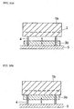
- FIG. 1 One specific example of a first aspect of the present invention in a heater module is depicted in Fig. 1.
- the heater module is furnished with heater part 1a in the interior of which a heating element 2 is formed, and block part 3a provided at the reverse side of heater part 1a to be shiftable up and down along guide shafts 4, wherein during heating heater part 1a and block part 3a are in abutment, as indicated in Fig. 1(a).
- heater part 1a and block part 3a are united to form a large-heat-capacity heater; and when it is to be cooled, block part 3a is, as depicted in Fig. 1(b), parted away from heater part 1a, descending toward the bottom part 5 of the equipment chamber. Accordingly, heat radiation is promoted, and the cooling speed of heater part 1a is hastened, by the fact that heater part 1a is left on its own with a smaller heat capacity.
- heater part 1b and block part 3b as shown in Fig. 2(a) are separated during heating, and during cooling block part 3b is, as indicated in Fig. 2(b), elevated to abut on the reverse side of heater part 1b, which is stationary.
- the abutting of block part 1b lets the cooling speed of heater part 1b be sped, because the heat in heater part 1b is transmitted to block part 3b, which has individuated heat capacity.
- block part 3c is stationary and heater part 1c shifts up and down along the guide shafts 4, apart from which the heater module is the same as that of Fig. 2.
- heater part 1c and block part 3c are as shown in Fig. 3(a) separated, and during cooling, by bringing down heater part 1c to abut on block part 3c on the bottom part 5 of the chamber, as indicated in Fig. 3(b), the heat in heater part 1c is transmitted to block part 3b.
- Factors influencing the transmission of heat from the heater part to the block part include contact resistance in the surfaces along which the heater part and block part abut. If the contact resistance is large, the isothermal properties and cooling speed of the heater part are liable to be affected because it takes time for heat to pass from the heater part. In light of this fact, forming through-holes in the top face of the block part or in the reverse face of the heater part and vacuum-chucking the two together under suction with a vacuum pump lets the abutment surfaces of the heater part and the block part adhere closely, dramatically lowering the contact resistance, which therefore is advantageous in improving the cooling speed of the heater part especially in the heater module in the second aspect.
- the block part separated from the heater part during heating is liable to be heated by radiant heat from the heater part.
- processing either or both of the matching abutment surfaces of the heater part and the block part into a specular surface makes reflecting back radiant heat from the heater part possible.
- the clearance between the heater part and the block part when heating is underway can be made smaller, which makes scaling-down the chamber as well as the equipment possible.
- the heater part in the present invention may be either a metal such as aluminum or a ceramic, but is preferably a ceramic in which a heating element is formed.
- the ceramic constituting the heater part is at least one selected from the group consisting of aluminum oxide, aluminum nitride, silicon nitride, silicon carbide, and boron nitride.
- metal or ceramic whose thermal conductivity is high may be utilized for the block part; preferable are, for example, Al, Mg, Cu, Fe, stainless steel, aluminum oxide, aluminum nitride, silicon nitride, silicon carbide, and boron nitride.
- the block part is either identical or similar to the heater part in form, and in that its diameter is within ⁇ 25% of the diameter of the heater part.
- the heat capacity of the block part preferably is 20% or more of the total heat capacity of the heater part and the block part.
- the cooling speed of conventional heaters has generally been at the 1°C/min level, because it has been dependent solely on radiant heat from a heater having a certain heat capacity.
- the cooling speed of the heater part although it depends on the heat capacity of the block part, is enhanced to at least several times the conventional level.
- cooling speeds of 10°C/min or more can be achieved if the heat capacity of the block part is designed to be 20% or more of the total heat capacity of the heater part and the block part, enabling productivity to be dramatically improved. What is more, such improvement in cooling speed means that in terms of wafers, enhancement in the adhesive strength of thin films, enhancement in mechanical hardness, and enhancement in etching characteristics can be anticipated.
- a heater module of the present invention as described above in CVD equipment employed in deposition of metal films as well as dielectric films, in etcher equipment employed in etching metal films as well as dielectric films, in coater/developer equipment employed in thermosetting of photoresists in photolithography, and in low- k dielectric baking devices employed in heating/baking of low- k films is especially efficacious owing to the effect of enhanced heater cooling speed.
- semiconductor manufacturing equipment in which a heater module of the present invention is utilized is a means that can serve to heighten productivity and reduce costs, and by which improvement in both characteristics and performance of wafers and other processed articles is recognizable.
- Block parts made from each of the metal and ceramic materials set forth in the following table and having the same diameter as the foregoing heater parts, were also fabricated. In doing so, the percent heat capacity of the block part with respect to the total heat capacity of the heater and block parts was varied as indicated in the table below by varying the block part thickness. In addition, in all samples, the top face of the block part (the face where it abuts with the heater part) was surfaced by lapping.
- Heater modules in the first aspect according to the present invention were assembled using these heater parts and block parts. That is, they were lent a structure in which during heating the heater part and the block part abut, and in which during cooling the block part is lowered to separate it from the heater part. It should be understood that elevation of the block part and its abutment onto/fixing against the heater part was by means of oil pressure or air pressure, and furthermore that with Sample 6 only, the heater part and the block part were held fast by vacuum-chucking. It should also be understood that the distance between the heater part and the block part separated during cooling was fixed at 200 mm with all of the samples.
- Isothermal ratings for each of the sample heater modules having been heated were found by applying a 200-V voltage to the heater part in abutment with the block part and heating to 200°C, maintaining that temperature for 10 minutes, and then measuring the temperature at 9 points within the top face (wafer-carrying surface) of the heater module. After that the block part was lowered to separate it from the heater part, and the speed with which the isolated heater part, left to radiate heat, cooled down to 150°C was measured. In doing so, isothermal ratings when cooled (150°C) were found from the temperatures at the 9 points within the top face likewise as just noted. These results were tabulated and set forth in the following table.
- a heater part the same as that of the foregoing Embodiment 1 was prepared, and an air-cool cooling block, made of aluminum, having a 60 liter/min capacity was installed on the heater part, fixed on the reverse face thereof. It will be appreciated that a block part was not used in the comparative example.
- This heater that has been in use to date was heated to 200°C, which temperature was maintained for 10 minutes, and then was cooled down to 150°C by means of the air-cool cooling block.
- isothermal rating when heated and when cooled was found in the same way as in Embodiment 1.
- the results were a heater cooling speed of 1°C/min, and an isothermal rating of ⁇ 1.5% when heated and ⁇ 1.7% when cooled, which was considerably inferior to that of the samples of the present invention in the foregoing Embodiment 1.
- a heater module was assembled utilizing the same heater part and block part as with Sample 4 in the foregoing Embodiment 1, but the reverse face of the AlN-made heater part-i.e., the face where it abuts with the Al-made block part-was covered with a Cu layer 0.2 mm in thickness.
- a heater module was assembled utilizing the same heater part and block part as with Sample 4 in the foregoing Embodiment 1, but the top face of the Al-made block part-i.e., the face where it abuts with the AlN-made heater part-was finished to a specular surface by a polishing process.
- the isothermal rating of the heater part having been heated was found by heating it in isolation to 200°C, maintaining that temperature for 10 minutes, and thereafter measuring its temperature at 9 points within the top face. Subsequently, the block part was lifted to abut it on the heater part, the heater part was allowed to cool down to 150°C, and the cooling speed was measured and the isothermal rating when cooled (150°C) was found.
- the heater module represented in Fig. 3, in the second aspect of the present invention was assembled utilizing the same heater part and block part as with Sample 4 in the foregoing Embodiment 1, but the heater part was installed to be shiftable up and down by means of oil pressure. That is, the heater module was lent a structure in which during heating the heater part and the block part are separated and the block part is brought into contact with, and rested on, the bottom part of the chamber, and during cooling, the heater part is lowered to abut on the heater part. It should be understood that the remaining aspects of the heater module were exactly the same as with Sample 4 in Embodiment 1.
- the isothermal rating of the heater part having been heated was found by heating it in isolation to 200°C, maintaining that temperature for 10 minutes, and thereafter measuring its temperature at 9 points within the top face. Subsequently, the heater part was lowered to abut it on the block part, the heater part was allowed to cool down to 150°C, and the cooling speed was measured and the isothermal rating when cooled (150°C) was found.
- Heater modules identical with those of the foregoing Embodiment 4 and comparative example were installed into place within a low- k film baking device, and an actual-practice implementation was made in which a low- k film coated onto a 12-inch Si wafer was cured.
- the low- k film adhesive strength improved 20% by comparison with the case with the baking device utilizing the heater module of the comparative example.
- the time for the heater to cool was curtailed to 1/25 by comparison with the comparative example.
- a heater module may be rendered in which the cooling speed of the heater post-heating may be heightened several times or more, preferentially 10 times or more, than conventional, and that can contribute toward bettering and improving productivity. What is more, utilizing the heater module lets semiconductor manufacturing equipment be scaled down, and makes appreciable cost reduction possible.
Landscapes
- Resistance Heating (AREA)
- Container, Conveyance, Adherence, Positioning, Of Wafer (AREA)
- Exposure Of Semiconductors, Excluding Electron Or Ion Beam Exposure (AREA)
- Chemical Vapour Deposition (AREA)
- Drying Of Semiconductors (AREA)
Abstract
Heater module, and semiconductor manufacturing equipment in which the heater module is utilized, for raising the cooling speed of a post-heating heater markedly more than conventional, and that can contribute toward bettering and improving productivity, without accompanying scaling-up of and cost increases in the semiconductor manufacturing equipment. <??>The heater module is furnished with heater part 1a for controlled heating of a wafer placed on its top face, and block part 3a provided to be shiftable relative to said heater part, for varying heat capacity in total with heater part 1a by abutting on or separating from the reverse surface of heater part 1a. By having the heat capacity of block part 1b be 20% or more of the total heat capacity of heater part 1a and block part 1b, the heater cooling speed can be made 10 DEG C/min or more. <IMAGE> <IMAGE>
Description
The present invention relates to heater modules, utilized in
semiconductor manufacturing tools that process semiconductor wafers, for
semiconductor manufacturing equipment capable of heat-treating and cooling
wafers, and to semiconductor manufacturing equipment in which such heater
modules are installed.
In the course of semiconductor fabrication, processes in which after being
treated by heating wafers are cooled include: thermosetting of photoresists in
photolithography with coater/developers; heating/baking of low-dielectric-constant,
i.e. low-k, insulating films; CVD film deposition in forming metal
interconnects and dielectric layers; and processes in etchers.
Heat-treatment of the wafers in these processes has conventionally been
carried out using heaters made of aluminum or ceramic. In particular, wafers
are placed onto the outer face of heaters in which a heating element is formed,
utilized to control heating while the wafers undergo processes such as
thermosetting of photoresists and heating/baking of low-k films, or CVD film
deposition and etching.
Recently, in order to enhance productivity in these processes, it has
become necessary to raise cooling speed for the post-heating heaters. By the
same token, designing for rapid cooling of the processed articles to improve
their characteristics has become widespread, and in particular, accompanying
the enlarging of wafer diametric span demands for enhanced cooling speed have
been growing.
Forcible liquid cooling and air cooling have been adopted in order to
rapidly cool the heater in semiconductor manufacturing equipment applications
to date. In specific terms, a cooling block is installed on the heater, usually on
the reverse side, and by circulating through the block a liquid or air as a heat-transferring
medium for cooling, heat is carried away from the heater,
heightening the cooling speed.
Nevertheless, with these forcible liquid cooling and air cooling systems,
the fact that large-scale devices are necessary for circulating the heat-transferring
medium and for radiating heat has proved to be a cost-increasing
factor in semiconductor manufacturing. Likewise, with it not being possible to
enlarge the capacity for the heat-transferring medium within the limited space
of the heater, significant improvement in heater cooling speed has been
difficult.
An object of the present invention, in view of such circumstances to date,
is to render a heater module, and semiconductor manufacturing equipment in
which the heater module is utilized, that makes it possible to raise markedly
the cooling speed of a post-heating heater, and that contributes toward
bettering and improving productivity, without accompanying scaling-up of and
cost increases in the semiconductor manufacturing equipment.
In order to achieve the foregoing objective, for semiconductor
manufacturing equipment a heater module that the present invention renders
is characterized in being provided with a heater part for controlled heating of a
wafer placed on its outer face, and a block part furnished to be shiftable relative
to the heater part, for varying heat capacity in total with the heater part by
abutting on and separating from the reverse side of the heater part. In
particular, the heat capacity of the block part is 20% or more of the total heat
capacity of the heater part and the block part.
An advantage of the foregoing heater module of the present invention for
semiconductor manufacturing equipment is in a first aspect that during
heating the heater part and the block part are brought into abutment, and
during cooling, by the block part being relatively shift-separated from the
heater part, the cooling speed of the heater part is quickened. Another
advantage is in a second aspect that during heating the heater part and the
block part are separated, and during cooling, by the block part and the heater
part being shifted relatively into abutment to conduct heat into the block part,
the cooling speed of the heater part is quickened.
With the foregoing heater module of the present invention for
semiconductor manufacturing equipment, when the heater part and the block
part are in abutment, the block part is preferably fixed to the heater part by
vacuum-chucking it thereto. In addition, at least one of either of the abutment
surfaces along which the heater part and the block part abut on each other
preferably is a specular surface.
Furthermore, with the foregoing heater module of the present invention
for semiconductor manufacturing equipment, the block part may be affixed to
the chamber bottom part in the semiconductor manufacturing equipment, or
else may be shifted into abutment on the chamber bottom part. In that case, the
chamber bottom part preferably is water-cooled.
In the foregoing heater module of the present invention for
semiconductor manufacturing equipment, the heater part preferably is a
ceramic in which a heating element is formed. The ceramic is preferably at least
one selected from the group consisting of aluminum oxide, aluminum nitride,
silicon nitride, silicon carbide, and boron nitride.
In addition, in the foregoing heater module of the present invention for
semiconductor manufacturing equipment, the block part is preferably at least
one selected from the group consisting of aluminum, magnesium, copper, iron,
stainless steel, aluminum oxide, aluminum nitride, silicon nitride, silicon
carbide, and boron nitride.
The foregoing heater module of the present invention for semiconductor
manufacturing equipment is preferably utilized in CVD equipment, etcher
equipment, coater/developer equipment, or a low-k dielectric baking device.
Furthermore, the present invention renders semiconductor
manufacturing equipment characterized in that installed therein is an above-described
heater module of the present invention for semiconductor
manufacturing equipment.
When a heater that has been heated is being cooled, its heat capacity is
what affects the cooling speed. The larger the heat capacity of the heater is, the
slower the cooling speed will be; conversely, the smaller the heat capacity is, the
faster the cooling speed will be. Conceivable as a means of lessening the heat
capacity of the heater with the objective of raising the cooling speed would be
thinning the heater thickness.
Meanwhile, wafers must be heated uniformly, and owing to the
consequent demand that the wafer-carrying surface of the heater be highly
isothermal, exploiting the thickness of the heater to spread the heat generated
by heating element uniformly in all directions is desirable. Still, thinning the
thickness of a heater in order to heighten its cooling speed gives rise to
problems in that its effectiveness in spreading heat uniformly is reduced, and
the isothermal properties in the wafer-carrying surface of the heater are
harmed.
To address this situation, the present invention provides a heater part for
controlled heating of a wafer placed on its outer face and, shiftable relative to
the heater part, a block part that may be abutted on as well as separated from
the reverse side of the heater part. With a heater module configured in this way
by the heater part and block part, the total heat capacity of the heater part and
the block part may be changed by the block part being in abutment against, and
with it being separated from, the reverse side of the heater part, and exploiting
this varying of the total heat capacity enables bettering and enhancing both the
isothermal properties, and at the same time the cooling speed, of the heater.
In particular, having the heat capacity of the block part be 20% or more of
the total heat capacity of the heater part and the block part makes even more
heat be transmitted from the heater to the block part being in abutment on the
heater, or else enables even more heat to be diffused to the surroundings from
the heater being parted off the block part, on account of which cooling speeds
that are all the higher may be looked forward to. It will be appreciated that the
larger the heat capacity of the block part, the more the cooling speed of the
heater part may be boosted. Nevertheless, inasmusch as enlarging the heat
capacity of the block part means that the chamber-and the equipment as a
whole-must be enlarged as well, the heat capacity of the block part must be
planned taking into consideration the goal of cooling speed enhancement and
the economics of the equipment overall.
One specific example of a first aspect of the present invention in a heater
module is depicted in Fig. 1. The heater module is furnished with heater part 1a
in the interior of which a heating element 2 is formed, and block part 3a
provided at the reverse side of heater part 1a to be shiftable up and down along
guide shafts 4, wherein during heating heater part 1a and block part 3a are in
abutment, as indicated in Fig. 1(a).
When the heater module is to heat, heater part 1a and block part 3a are
united to form a large-heat-capacity heater; and when it is to be cooled, block
part 3a is, as depicted in Fig. 1(b), parted away from heater part 1a, descending
toward the bottom part 5 of the equipment chamber. Accordingly, heat radiation
is promoted, and the cooling speed of heater part 1a is hastened, by the fact that
heater part 1a is left on its own with a smaller heat capacity.
Likewise, in the specific instance illustrated in Fig. 2 for example, as the
heater module in a second aspect, heater part 1b and block part 3b as shown in
Fig. 2(a) are separated during heating, and during cooling block part 3b is, as
indicated in Fig. 2(b), elevated to abut on the reverse side of heater part 1b,
which is stationary. The abutting of block part 1b lets the cooling speed of
heater part 1b be sped, because the heat in heater part 1b is transmitted to
block part 3b, which has individuated heat capacity.
In a heater module depicted in Fig. 3, further in the second aspect of the
present invention, block part 3c is stationary and heater part 1c shifts up and
down along the guide shafts 4, apart from which the heater module is the same
as that of Fig. 2. In particular, during heating, heater part 1c and block part 3c
are as shown in Fig. 3(a) separated, and during cooling, by bringing down
heater part 1c to abut on block part 3c on the bottom part 5 of the chamber, as
indicated in Fig. 3(b), the heat in heater part 1c is transmitted to block part 3b.
Factors influencing the transmission of heat from the heater part to the
block part include contact resistance in the surfaces along which the heater part
and block part abut. If the contact resistance is large, the isothermal properties
and cooling speed of the heater part are liable to be affected because it takes
time for heat to pass from the heater part. In light of this fact, forming
through-holes in the top face of the block part or in the reverse face of the heater
part and vacuum-chucking the two together under suction with a vacuum pump
lets the abutment surfaces of the heater part and the block part adhere closely,
dramatically lowering the contact resistance, which therefore is advantageous
in improving the cooling speed of the heater part especially in the heater
module in the second aspect.
Furthermore, with the heater module in the second aspect in particular,
the block part separated from the heater part during heating is liable to be
heated by radiant heat from the heater part. Given this situation, processing
either or both of the matching abutment surfaces of the heater part and the
block part into a specular surface makes reflecting back radiant heat from the
heater part possible. As a result, the clearance between the heater part and the
block part when heating is underway can be made smaller, which makes
scaling-down the chamber as well as the equipment possible.
What is more, if the heat that is transmitted to the block part is retained
as such, improvement in the cooling speed of the heater part could not be
expected because the heat that is transmitted from the heater part when
cooling is next underway would be kept from being adequately absorbed. For
that reason, it is preferable that after the block part undergoes transmission of
heat in contact with the heater part it is parted from the heater part and
brought into contact with the bottom part of the chamber to send its heat into
the chamber bottom part, whereby the block part cools quickly, readying it for
the next cooling. In that case, time to make ready for the next cooling may be
shortened by water-cooling the chamber bottom part.
Here, it is preferable to employ oil pressure or air pressure in abutting as
well as separating the heater part and block part, because doing so lets the
heater part as well as the block part be shifted smoothly.
The heater part in the present invention may be either a metal such as
aluminum or a ceramic, but is preferably a ceramic in which a heating element
is formed. Preferable as the ceramic constituting the heater part is at least one
selected from the group consisting of aluminum oxide, aluminum nitride, silicon
nitride, silicon carbide, and boron nitride.
Because both thermal and mechanical shock is exerted on the boundary
surface of the heater part in abutting with the block part, the chances are high
that cracking and like troubles will arise in the heater part with it being
ceramic. Owing to this likelihood, such shock can be mitigated by covering with
metal a surface of the heater part made from ceramic-at least the face that
abuts with the block part-to prevent cracking or the like in the heater part.
Meanwhile, metal or ceramic whose thermal conductivity is high may be
utilized for the block part; preferable are, for example, Al, Mg, Cu, Fe, stainless
steel, aluminum oxide, aluminum nitride, silicon nitride, silicon carbide, and
boron nitride.
It is also preferable that the block part is either identical or similar to the
heater part in form, and in that its diameter is within ±25% of the diameter of
the heater part. And it will be appreciated that as stated above, the heat
capacity of the block part preferably is 20% or more of the total heat capacity of
the heater part and the block part.
The cooling speed of conventional heaters has generally been at the
1°C/min level, because it has been dependent solely on radiant heat from a
heater having a certain heat capacity. In contrast, in a heater module as defined
by the present invention the cooling speed of the heater part, although it
depends on the heat capacity of the block part, is enhanced to at least several
times the conventional level. Specifically, cooling speeds of 10°C/min or more
can be achieved if the heat capacity of the block part is designed to be 20% or
more of the total heat capacity of the heater part and the block part, enabling
productivity to be dramatically improved. What is more, such improvement in
cooling speed means that in terms of wafers, enhancement in the adhesive
strength of thin films, enhancement in mechanical hardness, and enhancement
in etching characteristics can be anticipated.
Another consideration is that in situations where a heater is cooled by
heat radiation, with cooling speed being influenced by surface area, the
temperature in the vicinity of the heater lateral side has a greater tendency to
drop because the surface area there is generally large compared with the
middle portion, and during cooling the isothermal quality is consequently liable
to deteriorate. With a heater module as given by the present invention, however,
the heater part cools at a speed quite significantly faster than the speed of
cooling through the lateral side, and especially with the heater module in the
second aspect, because heat passes to the block part by means of thermal
conduction the isothermal quality during cooling is enhanced by a wide margin.
In concrete terms, by optimizing the heater- and block-part parameters, it is
possible to obtain an isothermal rating during cooling of within ±1%.
Utilizing a heater module of the present invention as described above in
CVD equipment employed in deposition of metal films as well as dielectric films,
in etcher equipment employed in etching metal films as well as dielectric films,
in coater/developer equipment employed in thermosetting of photoresists in
photolithography, and in low-k dielectric baking devices employed in
heating/baking of low-k films is especially efficacious owing to the effect of
enhanced heater cooling speed.
What is more, semiconductor manufacturing equipment in which a
heater module of the present invention is utilized is a means that can serve to
heighten productivity and reduce costs, and by which improvement in both
characteristics and performance of wafers and other processed articles is
recognizable.
Sets of two disks 335 mm diameter and 10 mm thickness made of the
ceramic materials set forth in the table below were prepared, and on the top
face of one disk in each set a heating element was formed by tungsten
metallization. Onto this ceramic disk the remaining ceramic disk in each set
was overlaid, putting the heating element into a sandwich which was then hot-press
joined using a hot press device, whereby ceramic heater parts were
fabricated.
Block parts, made from each of the metal and ceramic materials set forth
in the following table and having the same diameter as the foregoing heater
parts, were also fabricated. In doing so, the percent heat capacity of the block
part with respect to the total heat capacity of the heater and block parts was
varied as indicated in the table below by varying the block part thickness. In
addition, in all samples, the top face of the block part (the face where it abuts
with the heater part) was surfaced by lapping.
Heater modules in the first aspect according to the present invention
were assembled using these heater parts and block parts. That is, they were
lent a structure in which during heating the heater part and the block part abut,
and in which during cooling the block part is lowered to separate it from the
heater part. It should be understood that elevation of the block part and its
abutment onto/fixing against the heater part was by means of oil pressure or air
pressure, and furthermore that with Sample 6 only, the heater part and the
block part were held fast by vacuum-chucking. It should also be understood that
the distance between the heater part and the block part separated during
cooling was fixed at 200 mm with all of the samples.
Isothermal ratings for each of the sample heater modules having been
heated (200°C) were found by applying a 200-V voltage to the heater part in
abutment with the block part and heating to 200°C, maintaining that
temperature for 10 minutes, and then measuring the temperature at 9 points
within the top face (wafer-carrying surface) of the heater module. After that the
block part was lowered to separate it from the heater part, and the speed with
which the isolated heater part, left to radiate heat, cooled down to 150°C was
measured. In doing so, isothermal ratings when cooled (150°C) were found from
the temperatures at the 9 points within the top face likewise as just noted.
These results were tabulated and set forth in the following table.
| Sample | Heater part material | Block part material | Percent heat capacity | Shifting & holding fast | Cooling speed (°C/min) | Isothermal rating (±%) | ||
| When heated | When cooled | |||||||
| 1 | | Al | 5 | Oil press. | 5 | 0.5 | 0.7 | |
| 2 | AlN | Al | 15 | Oil press. | 7 | 0.5 | 0.7 | |
| 3 | AlN | Al | 20 | Oil press. | 10 | 0.5 | 0.7 | |
| 4 | AlN | Al | 100 | Oil press. | 25 | 0.5 | 0.7 | |
| 5 | AlN | Al | 200 | Oil press. | 32 | 0.5 | 0.7 | |
| 6 | AlN | Al | 100 | Vac. chuck. | 27 | 0.5 | 0.7 | |
| 7 | AlN | Al | 100 | Air press. | 25 | 0.5 | 0.7 | |
| 8 | SiC | Al | 100 | Oil press. | 23 | 0.6 | 0.8 | |
| 9 | Si3N4 | Al | 100 | Oil press. | 26 | 0.9 | 0.95 | |
| 10 | Al2O3 | Al | 100 | Oil press. | 21 | 0.9 | 0.95 | |
| 11 | BN | Al | 100 | Oil press. | 33 | 0.4 | 0.6 | |
| 12 | AlN | Mg | 100 | Oil press. | 22 | 0.5 | 0.7 | |
| 13 | AlN | Cu | 100 | Oil press. | 28 | 0.5 | 0.7 | |
| 14 | AlN | Fe | 100 | Oil press. | 20 | 0.5 | 0.7 | |
| 15 | AlN | SUS | 100 | Oil press. | 18 | 0.5 | 0.7 | |
| 16 | AlN | Al2O3 | 100 | Oil press. | 18 | 0.5 | 0.7 | |
| 17 | AlN | AlN | 100 | Oil press. | 22 | 0.5 | 0.7 | |
| 18 | AlN | Si3N4 | 100 | Oil press. | 18 | 0.5 | 0.7 | |
| 19 | AlN | AlN | 100 | Oil press. | 23 | 0.5 | 0.7 | |
| 20 | AlN | BN | 100 | Oil press. | 23 | 0.5 | 0.7 |
From the foregoing results, it is evident that with whichever of the
samples as heater modules by the present invention high heater-cooling speeds
of several °C/min or faster were obtained, and that isothermal ratings of within
±1% when heated and when cooled were sustained. In particular, it is evident
that by making the percent heat capacity of the block part 20% or less,
extremely high heater-cooling speeds of 10°C/min or more can be achieved even
as superior isothermal ratings are maintained.
A heater part the same as that of the foregoing Embodiment 1 was
prepared, and an air-cool cooling block, made of aluminum, having a 60
liter/min capacity was installed on the heater part, fixed on the reverse face
thereof. It will be appreciated that a block part was not used in the comparative
example. This heater that has been in use to date was heated to 200°C, which
temperature was maintained for 10 minutes, and then was cooled down to
150°C by means of the air-cool cooling block.
In that instance, isothermal rating when heated and when cooled (150°C)
was found in the same way as in Embodiment 1. The results were a heater
cooling speed of 1°C/min, and an isothermal rating of ±1.5% when heated and
±1.7% when cooled, which was considerably inferior to that of the samples of the
present invention in the foregoing Embodiment 1.
A heater module was assembled utilizing the same heater part and block
part as with Sample 4 in the foregoing Embodiment 1, but the reverse face of
the AlN-made heater part-i.e., the face where it abuts with the Al-made block
part-was covered with a Cu layer 0.2 mm in thickness.
The same testing and evaluation as with Embodiment 1 were performed
on this heater module, with the result being that the heater cooling speed and
the isothermal rating were the same as with Sample 4 in Embodiment 1. With
Sample 4 in Embodiment 1, however, at 500 cycles chips 0.1-0.2 mm in diameter
appeared in the edge of the reverse face of the heater part, but with the present
Embodiment 2 sample, no chips or like flaws were discernable at all.
A heater module was assembled utilizing the same heater part and block
part as with Sample 4 in the foregoing Embodiment 1, but the top face of the
Al-made block part-i.e., the face where it abuts with the AlN-made heater
part-was finished to a specular surface by a polishing process.
The same testing and evaluation as with Embodiment 1 was performed
on this heater module. Thanks to the top face of the block part having been
made mirror-like, heat radiant from the heater part was reflected back, keeping
the block part from absorbing the heat, and therefore even with the separation
between the heater part and the block part curtailed to 50 mm, the same heater
cooling speed and isothermal rating as with Sample 4 in Embodiment 1, where
the heater part-block part separation was set at 200 mm, were obtained.
The heater module represented in Fig. 2, in the second aspect of the
present invention, was assembled utilizing the same heater part and block part
as with Sample 4 in the foregoing Embodiment 1, but the block part was
installed to be shiftable up and down by means of oil pressure. That is, the
heater module was lent a structure in which during heating the heater part and
the block part are separated and the block part is brought into contact with, and
rested on, the bottom part of the chamber, and during cooling, the block part is
lifted to abut on the heater part. It should be understood that the remaining
aspects of the heater module were exactly the same as with Sample 4 in
Embodiment 1.
The isothermal rating of the heater part having been heated (200°C) was
found by heating it in isolation to 200°C, maintaining that temperature for 10
minutes, and thereafter measuring its temperature at 9 points within the top
face. Subsequently, the block part was lifted to abut it on the heater part, the
heater part was allowed to cool down to 150°C, and the cooling speed was
measured and the isothermal rating when cooled (150°C) was found.
The results were that the heater cooling speed and isothermal rating
were the same as with Sample 4 in Embodiment 1. However, with the block part,
which had been lowered until it contacted the chamber bottom part, cooled
down to room temperature the time until preparation for the next cooling of the
heater completed was shortened to 1/3 by comparison with Sample 4 in
Embodiment 1.
The heater module represented in Fig. 3, in the second aspect of the
present invention, was assembled utilizing the same heater part and block part
as with Sample 4 in the foregoing Embodiment 1, but the heater part was
installed to be shiftable up and down by means of oil pressure. That is, the
heater module was lent a structure in which during heating the heater part and
the block part are separated and the block part is brought into contact with, and
rested on, the bottom part of the chamber, and during cooling, the heater part is
lowered to abut on the heater part. It should be understood that the remaining
aspects of the heater module were exactly the same as with Sample 4 in
Embodiment 1.
The isothermal rating of the heater part having been heated (200°C) was
found by heating it in isolation to 200°C, maintaining that temperature for 10
minutes, and thereafter measuring its temperature at 9 points within the top
face. Subsequently, the heater part was lowered to abut it on the block part, the
heater part was allowed to cool down to 150°C, and the cooling speed was
measured and the isothermal rating when cooled (150°C) was found.
The results were that the heater cooling speed and isothermal rating
were the same as with Sample 4 in Embodiment 1. However, with the block part,
resting on and in constant contact with the chamber bottom part, cooled down
to room temperature the time until preparation for the next cooling of the
heater completed was shortened to 1/3 by comparison with Sample 4 in
Embodiment 1.
Heater modules identical with those of the foregoing Embodiment 4 and
comparative example were installed into place within a low-k film baking
device, and an actual-practice implementation was made in which a low-k film
coated onto a 12-inch Si wafer was cured.
With the low-k film cured in the baking device utilizing the heater
module of Embodiment 4, the low-k film adhesive strength improved 20% by
comparison with the case with the baking device utilizing the heater module of
the comparative example. In addition, the time for the heater to cool was
curtailed to 1/25 by comparison with the comparative example.
As given by the present invention, for semiconductor manufacturing
equipment a heater module may be rendered in which the cooling speed of the
heater post-heating may be heightened several times or more, preferentially 10
times or more, than conventional, and that can contribute toward bettering and
improving productivity. What is more, utilizing the heater module lets
semiconductor manufacturing equipment be scaled down, and makes
appreciable cost reduction possible.
Claims (18)
- A heater module for semiconductor manufacturing equipment, characterized in being furnished with:a heater part for controlled heating of a wafer placed on an obverse face thereof; anda block part furnished to be shiftable relative to said heater part, for varying heat capacity in total with said heater part by abutting on or separating from a reverse surface of said heater part.
- A heater module for semiconductor manufacturing equipment as set forth in claim 1, characterized in that the heat capacity of said block part is 20% or more of the total heat capacity of said heater part and said block part.
- A heater module for semiconductor manufacturing equipment as set forth in claim 1 or 2, characterized in that during heating said heater part and said block part are brought into abutment, and during cooling, said block part is relatively shift-separated from said heater part to quicken the cooling speed of said heater part.
- A heater module for semiconductor manufacturing equipment as set forth in claim 1 or 2, characterized in that during heating said heater part and said block part are separated, and during cooling, said block part and said heater part are relatively shifted into abutment for conducting heat into said block part to quicken the cooling speed of said heater part.
- A heater module for semiconductor manufacturing equipment as set forth in any of claims 1 through 4, characterized in that when said heater part and said block part are in abutment, said block part is fixed to said heater part by vacuum-chucking said block part to said heater part.
- A heater module for semiconductor manufacturing equipment as set forth in any of claims 1 through 5, characterized in that at least one of either of abutting surfaces along which said heater part and said block part abut on each other is a specular surface.
- A heater module for semiconductor manufacturing equipment as set forth in any of claims 1 through 6, characterized in that said block part is affixed to a bottom part of a chamber in the semiconductor manufacturing equipment, or else shifts into abutment on the chamber bottom part.
- A heater module for semiconductor manufacturing equipment as set forth in claim 7, characterized in that the chamber bottom is water-cooled.
- A heater module for semiconductor manufacturing equipment as set forth in any of claims 1 through 8, characterized in that said heater part is a ceramic in which a heating element is formed.
- A heater module for semiconductor manufacturing equipment as set forth in claim 9, characterized in that the ceramic is at least one selected from the group consisting of aluminum oxide, aluminum nitride, silicon nitride, silicon carbide, and boron nitride.
- A heater module for semiconductor manufacturing equipment as set forth in claim 9 or 10, characterized in that at least a surface of said heater part that abuts with said block part is covered with metal.
- A heater module for semiconductor manufacturing equipment as set forth in any of claims 1 through 11, characterized in that said block part is at least one selected from the group consisting of aluminum, magnesium, copper, iron, stainless steel, aluminum oxide, aluminum nitride, silicon nitride, silicon carbide, and boron nitride.
- A heater module for semiconductor manufacturing equipment as set forth in any of claims 1 through 12, characterized in that said block part is either identical or similar to said heater part in form, and in that its diameter is within ±25% of that of said heater part.
- A heater module for semiconductor manufacturing equipment as set forth in any of claims 1 through 3, characterized in that either said heater part or said block part is shifted relative to the other by means of either oil pressure or air pressure.
- A heater module for semiconductor manufacturing equipment as set forth in any of claims 1 through 4, characterized in that the cooling speed of said heater part is 10°C/min or more.
- A heater module for semiconductor manufacturing equipment as set forth in any of claims 1 through 15, characterized in that its isothermal rating while a wafer set in place on said heater part is being cooled is within ±1%.
- A heater module for semiconductor manufacturing equipment as set forth in any of claims 1 through 16, characterized in being utilized in CVD equipment, etcher equipment, coater/developer equipment, or a low-k dielectric baking device.
- Semiconductor manufacturing equipment characterized in that installed therein is a heater module for semiconductor manufacturing equipment as set forth in any of claims 1 through 17.
Applications Claiming Priority (3)
| Application Number | Priority Date | Filing Date | Title |
|---|---|---|---|
| JP2002163747 | 2002-06-05 | ||
| JP2002163747A JP4311914B2 (en) | 2002-06-05 | 2002-06-05 | Heater module for semiconductor manufacturing equipment |
| PCT/JP2003/006239 WO2003105199A1 (en) | 2002-06-05 | 2003-05-19 | Heater module for semiconductor production system |
Publications (1)
| Publication Number | Publication Date |
|---|---|
| EP1511069A1 true EP1511069A1 (en) | 2005-03-02 |
Family
ID=29727551
Family Applications (1)
| Application Number | Title | Priority Date | Filing Date |
|---|---|---|---|
| EP03757191A Withdrawn EP1511069A1 (en) | 2002-06-05 | 2003-05-19 | Heater module for semiconductor production system |
Country Status (7)
| Country | Link |
|---|---|
| US (3) | US6963052B2 (en) |
| EP (1) | EP1511069A1 (en) |
| JP (2) | JP4311914B2 (en) |
| KR (1) | KR100584055B1 (en) |
| CN (1) | CN100353493C (en) |
| TW (1) | TWI281711B (en) |
| WO (1) | WO2003105199A1 (en) |
Families Citing this family (385)
| Publication number | Priority date | Publication date | Assignee | Title |
|---|---|---|---|---|
| JP4311914B2 (en) * | 2002-06-05 | 2009-08-12 | 住友電気工業株式会社 | Heater module for semiconductor manufacturing equipment |
| JP2005150506A (en) | 2003-11-18 | 2005-06-09 | Sumitomo Electric Ind Ltd | Semiconductor manufacturing equipment |
| JP2007201484A (en) * | 2004-11-30 | 2007-08-09 | Sumitomo Electric Ind Ltd | Wafer holder for wafer prober and wafer prober equipped with the same |
| JP3945527B2 (en) | 2004-11-30 | 2007-07-18 | 住友電気工業株式会社 | Wafer holder for wafer prober and wafer prober equipped with the same |
| JP3972944B2 (en) | 2005-09-12 | 2007-09-05 | 住友電気工業株式会社 | Ceramic heater and semiconductor manufacturing apparatus having the same |
| JP4497103B2 (en) | 2006-02-21 | 2010-07-07 | 住友電気工業株式会社 | Wafer holder, heater unit on which it is mounted, and wafer prober |
| JP4739132B2 (en) * | 2006-07-04 | 2011-08-03 | Okiセミコンダクタ株式会社 | Heat treatment apparatus and heat treatment method |
| JP5056228B2 (en) * | 2007-07-13 | 2012-10-24 | 住友電気工業株式会社 | Heater unit and semiconductor device manufacturing / inspection apparatus having the same |
| USD643055S1 (en) * | 2008-09-11 | 2011-08-09 | Asm Japan K.K. | Heater block for use in a semiconductor processing tool |
| US10378106B2 (en) | 2008-11-14 | 2019-08-13 | Asm Ip Holding B.V. | Method of forming insulation film by modified PEALD |
| US9394608B2 (en) | 2009-04-06 | 2016-07-19 | Asm America, Inc. | Semiconductor processing reactor and components thereof |
| JP5447123B2 (en) * | 2009-05-28 | 2014-03-19 | 住友電気工業株式会社 | Heater unit and apparatus provided with the same |
| US8802201B2 (en) | 2009-08-14 | 2014-08-12 | Asm America, Inc. | Systems and methods for thin-film deposition of metal oxides using excited nitrogen-oxygen species |
| JP5416570B2 (en) * | 2009-12-15 | 2014-02-12 | 住友電気工業株式会社 | Heating / cooling device and apparatus equipped with the same |
| JP5293718B2 (en) * | 2010-10-01 | 2013-09-18 | 東京エレクトロン株式会社 | Heat treatment apparatus, heat treatment method and storage medium |
| JP5605265B2 (en) * | 2011-02-24 | 2014-10-15 | 住友電気工業株式会社 | Heater unit for semiconductor manufacturing equipment |
| KR101324960B1 (en) * | 2011-04-26 | 2013-11-04 | 주식회사 탑 엔지니어링 | Chuck Assembly for Semiconductor Substrate Processing Device |
| JP5658083B2 (en) * | 2011-05-11 | 2015-01-21 | 株式会社Screenセミコンダクターソリューションズ | Temperature change system |
| US9312155B2 (en) | 2011-06-06 | 2016-04-12 | Asm Japan K.K. | High-throughput semiconductor-processing apparatus equipped with multiple dual-chamber modules |
| US10364496B2 (en) | 2011-06-27 | 2019-07-30 | Asm Ip Holding B.V. | Dual section module having shared and unshared mass flow controllers |
| US10854498B2 (en) | 2011-07-15 | 2020-12-01 | Asm Ip Holding B.V. | Wafer-supporting device and method for producing same |
| US20130023129A1 (en) | 2011-07-20 | 2013-01-24 | Asm America, Inc. | Pressure transmitter for a semiconductor processing environment |
| US9017481B1 (en) | 2011-10-28 | 2015-04-28 | Asm America, Inc. | Process feed management for semiconductor substrate processing |
| CN102637593B (en) * | 2012-03-19 | 2017-09-19 | 晶能光电(江西)有限公司 | A kind of method and apparatus that short annealing alloy is carried out to epitaxial wafer |
| US9659799B2 (en) | 2012-08-28 | 2017-05-23 | Asm Ip Holding B.V. | Systems and methods for dynamic semiconductor process scheduling |
| US9021985B2 (en) | 2012-09-12 | 2015-05-05 | Asm Ip Holdings B.V. | Process gas management for an inductively-coupled plasma deposition reactor |
| US10714315B2 (en) | 2012-10-12 | 2020-07-14 | Asm Ip Holdings B.V. | Semiconductor reaction chamber showerhead |
| US20160376700A1 (en) | 2013-02-01 | 2016-12-29 | Asm Ip Holding B.V. | System for treatment of deposition reactor |
| US9589770B2 (en) | 2013-03-08 | 2017-03-07 | Asm Ip Holding B.V. | Method and systems for in-situ formation of intermediate reactive species |
| US9484191B2 (en) | 2013-03-08 | 2016-11-01 | Asm Ip Holding B.V. | Pulsed remote plasma method and system |
| JP5630526B2 (en) * | 2013-04-08 | 2014-11-26 | 東京エレクトロン株式会社 | Heat treatment equipment |
| JP6088909B2 (en) * | 2013-06-04 | 2017-03-01 | 株式会社Screenセミコンダクターソリューションズ | Heat treatment equipment |
| CN104465453B (en) * | 2013-09-20 | 2018-10-30 | 住友电气工业株式会社 | The wafer heater of plasma CVD equipment |
| US9240412B2 (en) | 2013-09-27 | 2016-01-19 | Asm Ip Holding B.V. | Semiconductor structure and device and methods of forming same using selective epitaxial process |
| US10683571B2 (en) | 2014-02-25 | 2020-06-16 | Asm Ip Holding B.V. | Gas supply manifold and method of supplying gases to chamber using same |
| US10167557B2 (en) | 2014-03-18 | 2019-01-01 | Asm Ip Holding B.V. | Gas distribution system, reactor including the system, and methods of using the same |
| US11015245B2 (en) | 2014-03-19 | 2021-05-25 | Asm Ip Holding B.V. | Gas-phase reactor and system having exhaust plenum and components thereof |
| US10858737B2 (en) | 2014-07-28 | 2020-12-08 | Asm Ip Holding B.V. | Showerhead assembly and components thereof |
| US9890456B2 (en) | 2014-08-21 | 2018-02-13 | Asm Ip Holding B.V. | Method and system for in situ formation of gas-phase compounds |
| US10941490B2 (en) * | 2014-10-07 | 2021-03-09 | Asm Ip Holding B.V. | Multiple temperature range susceptor, assembly, reactor and system including the susceptor, and methods of using the same |
| US9657845B2 (en) | 2014-10-07 | 2017-05-23 | Asm Ip Holding B.V. | Variable conductance gas distribution apparatus and method |
| KR102263121B1 (en) | 2014-12-22 | 2021-06-09 | 에이에스엠 아이피 홀딩 비.브이. | Semiconductor device and manufacuring method thereof |
| US10529542B2 (en) | 2015-03-11 | 2020-01-07 | Asm Ip Holdings B.V. | Cross-flow reactor and method |
| US10276355B2 (en) | 2015-03-12 | 2019-04-30 | Asm Ip Holding B.V. | Multi-zone reactor, system including the reactor, and method of using the same |
| US10458018B2 (en) | 2015-06-26 | 2019-10-29 | Asm Ip Holding B.V. | Structures including metal carbide material, devices including the structures, and methods of forming same |
| US10600673B2 (en) | 2015-07-07 | 2020-03-24 | Asm Ip Holding B.V. | Magnetic susceptor to baseplate seal |
| US10083836B2 (en) | 2015-07-24 | 2018-09-25 | Asm Ip Holding B.V. | Formation of boron-doped titanium metal films with high work function |
| US9960072B2 (en) | 2015-09-29 | 2018-05-01 | Asm Ip Holding B.V. | Variable adjustment for precise matching of multiple chamber cavity housings |
| US10211308B2 (en) | 2015-10-21 | 2019-02-19 | Asm Ip Holding B.V. | NbMC layers |
| US10322384B2 (en) | 2015-11-09 | 2019-06-18 | Asm Ip Holding B.V. | Counter flow mixer for process chamber |
| US11139308B2 (en) | 2015-12-29 | 2021-10-05 | Asm Ip Holding B.V. | Atomic layer deposition of III-V compounds to form V-NAND devices |
| US10529554B2 (en) | 2016-02-19 | 2020-01-07 | Asm Ip Holding B.V. | Method for forming silicon nitride film selectively on sidewalls or flat surfaces of trenches |
| US10468251B2 (en) | 2016-02-19 | 2019-11-05 | Asm Ip Holding B.V. | Method for forming spacers using silicon nitride film for spacer-defined multiple patterning |
| US10501866B2 (en) | 2016-03-09 | 2019-12-10 | Asm Ip Holding B.V. | Gas distribution apparatus for improved film uniformity in an epitaxial system |
| US10343920B2 (en) | 2016-03-18 | 2019-07-09 | Asm Ip Holding B.V. | Aligned carbon nanotubes |
| US9892913B2 (en) | 2016-03-24 | 2018-02-13 | Asm Ip Holding B.V. | Radial and thickness control via biased multi-port injection settings |
| US10190213B2 (en) | 2016-04-21 | 2019-01-29 | Asm Ip Holding B.V. | Deposition of metal borides |
| US10865475B2 (en) | 2016-04-21 | 2020-12-15 | Asm Ip Holding B.V. | Deposition of metal borides and silicides |
| US10032628B2 (en) | 2016-05-02 | 2018-07-24 | Asm Ip Holding B.V. | Source/drain performance through conformal solid state doping |
| US10367080B2 (en) | 2016-05-02 | 2019-07-30 | Asm Ip Holding B.V. | Method of forming a germanium oxynitride film |
| KR102592471B1 (en) | 2016-05-17 | 2023-10-20 | 에이에스엠 아이피 홀딩 비.브이. | Method of forming metal interconnection and method of fabricating semiconductor device using the same |
| US11453943B2 (en) | 2016-05-25 | 2022-09-27 | Asm Ip Holding B.V. | Method for forming carbon-containing silicon/metal oxide or nitride film by ALD using silicon precursor and hydrocarbon precursor |
| US10388509B2 (en) | 2016-06-28 | 2019-08-20 | Asm Ip Holding B.V. | Formation of epitaxial layers via dislocation filtering |
| US10612137B2 (en) | 2016-07-08 | 2020-04-07 | Asm Ip Holdings B.V. | Organic reactants for atomic layer deposition |
| US9859151B1 (en) | 2016-07-08 | 2018-01-02 | Asm Ip Holding B.V. | Selective film deposition method to form air gaps |
| US10714385B2 (en) | 2016-07-19 | 2020-07-14 | Asm Ip Holding B.V. | Selective deposition of tungsten |
| KR102354490B1 (en) | 2016-07-27 | 2022-01-21 | 에이에스엠 아이피 홀딩 비.브이. | Method of processing a substrate |
| US9887082B1 (en) | 2016-07-28 | 2018-02-06 | Asm Ip Holding B.V. | Method and apparatus for filling a gap |
| KR102532607B1 (en) | 2016-07-28 | 2023-05-15 | 에이에스엠 아이피 홀딩 비.브이. | Substrate processing apparatus and method of operating the same |
| US9812320B1 (en) | 2016-07-28 | 2017-11-07 | Asm Ip Holding B.V. | Method and apparatus for filling a gap |
| US10395919B2 (en) | 2016-07-28 | 2019-08-27 | Asm Ip Holding B.V. | Method and apparatus for filling a gap |
| US10410943B2 (en) | 2016-10-13 | 2019-09-10 | Asm Ip Holding B.V. | Method for passivating a surface of a semiconductor and related systems |
| US10643826B2 (en) | 2016-10-26 | 2020-05-05 | Asm Ip Holdings B.V. | Methods for thermally calibrating reaction chambers |
| US11532757B2 (en) | 2016-10-27 | 2022-12-20 | Asm Ip Holding B.V. | Deposition of charge trapping layers |
| US10643904B2 (en) | 2016-11-01 | 2020-05-05 | Asm Ip Holdings B.V. | Methods for forming a semiconductor device and related semiconductor device structures |
| US10714350B2 (en) | 2016-11-01 | 2020-07-14 | ASM IP Holdings, B.V. | Methods for forming a transition metal niobium nitride film on a substrate by atomic layer deposition and related semiconductor device structures |
| US10435790B2 (en) | 2016-11-01 | 2019-10-08 | Asm Ip Holding B.V. | Method of subatmospheric plasma-enhanced ALD using capacitively coupled electrodes with narrow gap |
| US10229833B2 (en) | 2016-11-01 | 2019-03-12 | Asm Ip Holding B.V. | Methods for forming a transition metal nitride film on a substrate by atomic layer deposition and related semiconductor device structures |
| US10134757B2 (en) | 2016-11-07 | 2018-11-20 | Asm Ip Holding B.V. | Method of processing a substrate and a device manufactured by using the method |
| KR102546317B1 (en) | 2016-11-15 | 2023-06-21 | 에이에스엠 아이피 홀딩 비.브이. | Gas supply unit and substrate processing apparatus including the same |
| US10340135B2 (en) | 2016-11-28 | 2019-07-02 | Asm Ip Holding B.V. | Method of topologically restricted plasma-enhanced cyclic deposition of silicon or metal nitride |
| KR102762543B1 (en) | 2016-12-14 | 2025-02-05 | 에이에스엠 아이피 홀딩 비.브이. | Substrate processing apparatus |
| US11447861B2 (en) | 2016-12-15 | 2022-09-20 | Asm Ip Holding B.V. | Sequential infiltration synthesis apparatus and a method of forming a patterned structure |
| US11581186B2 (en) | 2016-12-15 | 2023-02-14 | Asm Ip Holding B.V. | Sequential infiltration synthesis apparatus |
| KR102700194B1 (en) | 2016-12-19 | 2024-08-28 | 에이에스엠 아이피 홀딩 비.브이. | Substrate processing apparatus |
| US10269558B2 (en) | 2016-12-22 | 2019-04-23 | Asm Ip Holding B.V. | Method of forming a structure on a substrate |
| US10867788B2 (en) | 2016-12-28 | 2020-12-15 | Asm Ip Holding B.V. | Method of forming a structure on a substrate |
| US11390950B2 (en) | 2017-01-10 | 2022-07-19 | Asm Ip Holding B.V. | Reactor system and method to reduce residue buildup during a film deposition process |
| JP6285586B2 (en) * | 2017-02-06 | 2018-02-28 | 株式会社Screenセミコンダクターソリューションズ | Heating plate cooling method |
| US10655221B2 (en) | 2017-02-09 | 2020-05-19 | Asm Ip Holding B.V. | Method for depositing oxide film by thermal ALD and PEALD |
| US10468261B2 (en) | 2017-02-15 | 2019-11-05 | Asm Ip Holding B.V. | Methods for forming a metallic film on a substrate by cyclical deposition and related semiconductor device structures |
| US10529563B2 (en) | 2017-03-29 | 2020-01-07 | Asm Ip Holdings B.V. | Method for forming doped metal oxide films on a substrate by cyclical deposition and related semiconductor device structures |
| US10283353B2 (en) | 2017-03-29 | 2019-05-07 | Asm Ip Holding B.V. | Method of reforming insulating film deposited on substrate with recess pattern |
| USD876504S1 (en) | 2017-04-03 | 2020-02-25 | Asm Ip Holding B.V. | Exhaust flow control ring for semiconductor deposition apparatus |
| KR102457289B1 (en) | 2017-04-25 | 2022-10-21 | 에이에스엠 아이피 홀딩 비.브이. | Method for depositing a thin film and manufacturing a semiconductor device |
| US10892156B2 (en) | 2017-05-08 | 2021-01-12 | Asm Ip Holding B.V. | Methods for forming a silicon nitride film on a substrate and related semiconductor device structures |
| US10770286B2 (en) | 2017-05-08 | 2020-09-08 | Asm Ip Holdings B.V. | Methods for selectively forming a silicon nitride film on a substrate and related semiconductor device structures |
| US10446393B2 (en) | 2017-05-08 | 2019-10-15 | Asm Ip Holding B.V. | Methods for forming silicon-containing epitaxial layers and related semiconductor device structures |
| US10504742B2 (en) | 2017-05-31 | 2019-12-10 | Asm Ip Holding B.V. | Method of atomic layer etching using hydrogen plasma |
| US10886123B2 (en) | 2017-06-02 | 2021-01-05 | Asm Ip Holding B.V. | Methods for forming low temperature semiconductor layers and related semiconductor device structures |
| US12040200B2 (en) | 2017-06-20 | 2024-07-16 | Asm Ip Holding B.V. | Semiconductor processing apparatus and methods for calibrating a semiconductor processing apparatus |
| US11306395B2 (en) | 2017-06-28 | 2022-04-19 | Asm Ip Holding B.V. | Methods for depositing a transition metal nitride film on a substrate by atomic layer deposition and related deposition apparatus |
| US10685834B2 (en) | 2017-07-05 | 2020-06-16 | Asm Ip Holdings B.V. | Methods for forming a silicon germanium tin layer and related semiconductor device structures |
| TWI794238B (en) | 2017-07-13 | 2023-03-01 | 荷蘭商Asm智慧財產控股公司 | Apparatus and method for removal of oxide and carbon from semiconductor films in a single processing chamber |
| KR20190009245A (en) | 2017-07-18 | 2019-01-28 | 에이에스엠 아이피 홀딩 비.브이. | Methods for forming a semiconductor device structure and related semiconductor device structures |
| US11374112B2 (en) | 2017-07-19 | 2022-06-28 | Asm Ip Holding B.V. | Method for depositing a group IV semiconductor and related semiconductor device structures |
| US10541333B2 (en) | 2017-07-19 | 2020-01-21 | Asm Ip Holding B.V. | Method for depositing a group IV semiconductor and related semiconductor device structures |
| US11018002B2 (en) | 2017-07-19 | 2021-05-25 | Asm Ip Holding B.V. | Method for selectively depositing a Group IV semiconductor and related semiconductor device structures |
| US10590535B2 (en) | 2017-07-26 | 2020-03-17 | Asm Ip Holdings B.V. | Chemical treatment, deposition and/or infiltration apparatus and method for using the same |
| US10605530B2 (en) | 2017-07-26 | 2020-03-31 | Asm Ip Holding B.V. | Assembly of a liner and a flange for a vertical furnace as well as the liner and the vertical furnace |
| US10312055B2 (en) | 2017-07-26 | 2019-06-04 | Asm Ip Holding B.V. | Method of depositing film by PEALD using negative bias |
| TWI815813B (en) | 2017-08-04 | 2023-09-21 | 荷蘭商Asm智慧財產控股公司 | Showerhead assembly for distributing a gas within a reaction chamber |
| US10770336B2 (en) | 2017-08-08 | 2020-09-08 | Asm Ip Holding B.V. | Substrate lift mechanism and reactor including same |
| US10692741B2 (en) | 2017-08-08 | 2020-06-23 | Asm Ip Holdings B.V. | Radiation shield |
| US11769682B2 (en) | 2017-08-09 | 2023-09-26 | Asm Ip Holding B.V. | Storage apparatus for storing cassettes for substrates and processing apparatus equipped therewith |
| US11139191B2 (en) | 2017-08-09 | 2021-10-05 | Asm Ip Holding B.V. | Storage apparatus for storing cassettes for substrates and processing apparatus equipped therewith |
| US10249524B2 (en) | 2017-08-09 | 2019-04-02 | Asm Ip Holding B.V. | Cassette holder assembly for a substrate cassette and holding member for use in such assembly |
| US10236177B1 (en) | 2017-08-22 | 2019-03-19 | ASM IP Holding B.V.. | Methods for depositing a doped germanium tin semiconductor and related semiconductor device structures |
| USD900036S1 (en) | 2017-08-24 | 2020-10-27 | Asm Ip Holding B.V. | Heater electrical connector and adapter |
| US11830730B2 (en) | 2017-08-29 | 2023-11-28 | Asm Ip Holding B.V. | Layer forming method and apparatus |
| US11295980B2 (en) | 2017-08-30 | 2022-04-05 | Asm Ip Holding B.V. | Methods for depositing a molybdenum metal film over a dielectric surface of a substrate by a cyclical deposition process and related semiconductor device structures |
| US11056344B2 (en) | 2017-08-30 | 2021-07-06 | Asm Ip Holding B.V. | Layer forming method |
| KR102491945B1 (en) | 2017-08-30 | 2023-01-26 | 에이에스엠 아이피 홀딩 비.브이. | Substrate processing apparatus |
| KR102401446B1 (en) | 2017-08-31 | 2022-05-24 | 에이에스엠 아이피 홀딩 비.브이. | Substrate processing apparatus |
| US10607895B2 (en) | 2017-09-18 | 2020-03-31 | Asm Ip Holdings B.V. | Method for forming a semiconductor device structure comprising a gate fill metal |
| KR102630301B1 (en) | 2017-09-21 | 2024-01-29 | 에이에스엠 아이피 홀딩 비.브이. | Method of sequential infiltration synthesis treatment of infiltrateable material and structures and devices formed using same |
| US10844484B2 (en) | 2017-09-22 | 2020-11-24 | Asm Ip Holding B.V. | Apparatus for dispensing a vapor phase reactant to a reaction chamber and related methods |
| US10658205B2 (en) | 2017-09-28 | 2020-05-19 | Asm Ip Holdings B.V. | Chemical dispensing apparatus and methods for dispensing a chemical to a reaction chamber |
| US10403504B2 (en) | 2017-10-05 | 2019-09-03 | Asm Ip Holding B.V. | Method for selectively depositing a metallic film on a substrate |
| US10319588B2 (en) | 2017-10-10 | 2019-06-11 | Asm Ip Holding B.V. | Method for depositing a metal chalcogenide on a substrate by cyclical deposition |
| US10923344B2 (en) | 2017-10-30 | 2021-02-16 | Asm Ip Holding B.V. | Methods for forming a semiconductor structure and related semiconductor structures |
| US10910262B2 (en) | 2017-11-16 | 2021-02-02 | Asm Ip Holding B.V. | Method of selectively depositing a capping layer structure on a semiconductor device structure |
| KR102443047B1 (en) | 2017-11-16 | 2022-09-14 | 에이에스엠 아이피 홀딩 비.브이. | Substrate processing apparatus method and apparatus manufactured thereby |
| US11022879B2 (en) | 2017-11-24 | 2021-06-01 | Asm Ip Holding B.V. | Method of forming an enhanced unexposed photoresist layer |
| TWI791689B (en) | 2017-11-27 | 2023-02-11 | 荷蘭商Asm智慧財產控股私人有限公司 | Apparatus including a clean mini environment |
| WO2019103613A1 (en) | 2017-11-27 | 2019-05-31 | Asm Ip Holding B.V. | A storage device for storing wafer cassettes for use with a batch furnace |
| US10290508B1 (en) | 2017-12-05 | 2019-05-14 | Asm Ip Holding B.V. | Method for forming vertical spacers for spacer-defined patterning |
| US10872771B2 (en) | 2018-01-16 | 2020-12-22 | Asm Ip Holding B. V. | Method for depositing a material film on a substrate within a reaction chamber by a cyclical deposition process and related device structures |
| US11482412B2 (en) | 2018-01-19 | 2022-10-25 | Asm Ip Holding B.V. | Method for depositing a gap-fill layer by plasma-assisted deposition |
| TWI799494B (en) | 2018-01-19 | 2023-04-21 | 荷蘭商Asm 智慧財產控股公司 | Deposition method |
| USD903477S1 (en) | 2018-01-24 | 2020-12-01 | Asm Ip Holdings B.V. | Metal clamp |
| US11018047B2 (en) | 2018-01-25 | 2021-05-25 | Asm Ip Holding B.V. | Hybrid lift pin |
| US10535516B2 (en) | 2018-02-01 | 2020-01-14 | Asm Ip Holdings B.V. | Method for depositing a semiconductor structure on a surface of a substrate and related semiconductor structures |
| USD880437S1 (en) | 2018-02-01 | 2020-04-07 | Asm Ip Holding B.V. | Gas supply plate for semiconductor manufacturing apparatus |
| US11081345B2 (en) | 2018-02-06 | 2021-08-03 | Asm Ip Holding B.V. | Method of post-deposition treatment for silicon oxide film |
| WO2019158960A1 (en) | 2018-02-14 | 2019-08-22 | Asm Ip Holding B.V. | A method for depositing a ruthenium-containing film on a substrate by a cyclical deposition process |
| US10896820B2 (en) | 2018-02-14 | 2021-01-19 | Asm Ip Holding B.V. | Method for depositing a ruthenium-containing film on a substrate by a cyclical deposition process |
| US10731249B2 (en) | 2018-02-15 | 2020-08-04 | Asm Ip Holding B.V. | Method of forming a transition metal containing film on a substrate by a cyclical deposition process, a method for supplying a transition metal halide compound to a reaction chamber, and related vapor deposition apparatus |
| US10658181B2 (en) | 2018-02-20 | 2020-05-19 | Asm Ip Holding B.V. | Method of spacer-defined direct patterning in semiconductor fabrication |
| KR102636427B1 (en) | 2018-02-20 | 2024-02-13 | 에이에스엠 아이피 홀딩 비.브이. | Substrate processing method and apparatus |
| US10975470B2 (en) | 2018-02-23 | 2021-04-13 | Asm Ip Holding B.V. | Apparatus for detecting or monitoring for a chemical precursor in a high temperature environment |
| US11473195B2 (en) | 2018-03-01 | 2022-10-18 | Asm Ip Holding B.V. | Semiconductor processing apparatus and a method for processing a substrate |
| US11629406B2 (en) | 2018-03-09 | 2023-04-18 | Asm Ip Holding B.V. | Semiconductor processing apparatus comprising one or more pyrometers for measuring a temperature of a substrate during transfer of the substrate |
| US11114283B2 (en) | 2018-03-16 | 2021-09-07 | Asm Ip Holding B.V. | Reactor, system including the reactor, and methods of manufacturing and using same |
| KR102646467B1 (en) | 2018-03-27 | 2024-03-11 | 에이에스엠 아이피 홀딩 비.브이. | Method of forming an electrode on a substrate and a semiconductor device structure including an electrode |
| US11230766B2 (en) | 2018-03-29 | 2022-01-25 | Asm Ip Holding B.V. | Substrate processing apparatus and method |
| US11088002B2 (en) | 2018-03-29 | 2021-08-10 | Asm Ip Holding B.V. | Substrate rack and a substrate processing system and method |
| US10510536B2 (en) | 2018-03-29 | 2019-12-17 | Asm Ip Holding B.V. | Method of depositing a co-doped polysilicon film on a surface of a substrate within a reaction chamber |
| KR102501472B1 (en) | 2018-03-30 | 2023-02-20 | 에이에스엠 아이피 홀딩 비.브이. | Substrate processing method |
| KR102600229B1 (en) | 2018-04-09 | 2023-11-10 | 에이에스엠 아이피 홀딩 비.브이. | Substrate supporting device, substrate processing apparatus including the same and substrate processing method |
| TWI843623B (en) | 2018-05-08 | 2024-05-21 | 荷蘭商Asm Ip私人控股有限公司 | Methods for depositing an oxide film on a substrate by a cyclical deposition process and related device structures |
| US12025484B2 (en) | 2018-05-08 | 2024-07-02 | Asm Ip Holding B.V. | Thin film forming method |
| US12272527B2 (en) | 2018-05-09 | 2025-04-08 | Asm Ip Holding B.V. | Apparatus for use with hydrogen radicals and method of using same |
| KR20190129718A (en) | 2018-05-11 | 2019-11-20 | 에이에스엠 아이피 홀딩 비.브이. | Methods for forming a doped metal carbide film on a substrate and related semiconductor device structures |
| KR102596988B1 (en) | 2018-05-28 | 2023-10-31 | 에이에스엠 아이피 홀딩 비.브이. | Method of processing a substrate and a device manufactured by the same |
| US11718913B2 (en) | 2018-06-04 | 2023-08-08 | Asm Ip Holding B.V. | Gas distribution system and reactor system including same |
| TWI840362B (en) | 2018-06-04 | 2024-05-01 | 荷蘭商Asm Ip私人控股有限公司 | Wafer handling chamber with moisture reduction |
| US11286562B2 (en) | 2018-06-08 | 2022-03-29 | Asm Ip Holding B.V. | Gas-phase chemical reactor and method of using same |
| US10797133B2 (en) | 2018-06-21 | 2020-10-06 | Asm Ip Holding B.V. | Method for depositing a phosphorus doped silicon arsenide film and related semiconductor device structures |
| KR102568797B1 (en) | 2018-06-21 | 2023-08-21 | 에이에스엠 아이피 홀딩 비.브이. | Substrate processing system |
| KR20250134000A (en) | 2018-06-27 | 2025-09-09 | 에이에스엠 아이피 홀딩 비.브이. | Cyclic deposition methods for forming metal-containing material and films and structures including the metal-containing material |
| WO2020003000A1 (en) | 2018-06-27 | 2020-01-02 | Asm Ip Holding B.V. | Cyclic deposition methods for forming metal-containing material and films and structures including the metal-containing material |
| US10612136B2 (en) | 2018-06-29 | 2020-04-07 | ASM IP Holding, B.V. | Temperature-controlled flange and reactor system including same |
| KR102686758B1 (en) | 2018-06-29 | 2024-07-18 | 에이에스엠 아이피 홀딩 비.브이. | Method for depositing a thin film and manufacturing a semiconductor device |
| US10755922B2 (en) | 2018-07-03 | 2020-08-25 | Asm Ip Holding B.V. | Method for depositing silicon-free carbon-containing film as gap-fill layer by pulse plasma-assisted deposition |
| US10388513B1 (en) | 2018-07-03 | 2019-08-20 | Asm Ip Holding B.V. | Method for depositing silicon-free carbon-containing film as gap-fill layer by pulse plasma-assisted deposition |
| US10767789B2 (en) | 2018-07-16 | 2020-09-08 | Asm Ip Holding B.V. | Diaphragm valves, valve components, and methods for forming valve components |
| US10483099B1 (en) | 2018-07-26 | 2019-11-19 | Asm Ip Holding B.V. | Method for forming thermally stable organosilicon polymer film |
| US11053591B2 (en) | 2018-08-06 | 2021-07-06 | Asm Ip Holding B.V. | Multi-port gas injection system and reactor system including same |
| US10883175B2 (en) | 2018-08-09 | 2021-01-05 | Asm Ip Holding B.V. | Vertical furnace for processing substrates and a liner for use therein |
| US10829852B2 (en) | 2018-08-16 | 2020-11-10 | Asm Ip Holding B.V. | Gas distribution device for a wafer processing apparatus |
| US11430674B2 (en) | 2018-08-22 | 2022-08-30 | Asm Ip Holding B.V. | Sensor array, apparatus for dispensing a vapor phase reactant to a reaction chamber and related methods |
| KR102707956B1 (en) | 2018-09-11 | 2024-09-19 | 에이에스엠 아이피 홀딩 비.브이. | Method for deposition of a thin film |
| US11024523B2 (en) | 2018-09-11 | 2021-06-01 | Asm Ip Holding B.V. | Substrate processing apparatus and method |
| US11049751B2 (en) | 2018-09-14 | 2021-06-29 | Asm Ip Holding B.V. | Cassette supply system to store and handle cassettes and processing apparatus equipped therewith |
| CN110970344B (en) | 2018-10-01 | 2024-10-25 | Asmip控股有限公司 | Substrate holding device, system including the same and method of using the same |
| US11232963B2 (en) | 2018-10-03 | 2022-01-25 | Asm Ip Holding B.V. | Substrate processing apparatus and method |
| KR102592699B1 (en) | 2018-10-08 | 2023-10-23 | 에이에스엠 아이피 홀딩 비.브이. | Substrate support unit and apparatuses for depositing thin film and processing the substrate including the same |
| US10847365B2 (en) | 2018-10-11 | 2020-11-24 | Asm Ip Holding B.V. | Method of forming conformal silicon carbide film by cyclic CVD |
| US10811256B2 (en) | 2018-10-16 | 2020-10-20 | Asm Ip Holding B.V. | Method for etching a carbon-containing feature |
| KR102546322B1 (en) | 2018-10-19 | 2023-06-21 | 에이에스엠 아이피 홀딩 비.브이. | Substrate processing apparatus and substrate processing method |
| KR102605121B1 (en) | 2018-10-19 | 2023-11-23 | 에이에스엠 아이피 홀딩 비.브이. | Substrate processing apparatus and substrate processing method |
| USD948463S1 (en) | 2018-10-24 | 2022-04-12 | Asm Ip Holding B.V. | Susceptor for semiconductor substrate supporting apparatus |
| US10381219B1 (en) | 2018-10-25 | 2019-08-13 | Asm Ip Holding B.V. | Methods for forming a silicon nitride film |
| US12378665B2 (en) | 2018-10-26 | 2025-08-05 | Asm Ip Holding B.V. | High temperature coatings for a preclean and etch apparatus and related methods |
| US11087997B2 (en) | 2018-10-31 | 2021-08-10 | Asm Ip Holding B.V. | Substrate processing apparatus for processing substrates |
| KR102748291B1 (en) | 2018-11-02 | 2024-12-31 | 에이에스엠 아이피 홀딩 비.브이. | Substrate support unit and substrate processing apparatus including the same |
| US11572620B2 (en) | 2018-11-06 | 2023-02-07 | Asm Ip Holding B.V. | Methods for selectively depositing an amorphous silicon film on a substrate |
| US11031242B2 (en) | 2018-11-07 | 2021-06-08 | Asm Ip Holding B.V. | Methods for depositing a boron doped silicon germanium film |
| US10818758B2 (en) | 2018-11-16 | 2020-10-27 | Asm Ip Holding B.V. | Methods for forming a metal silicate film on a substrate in a reaction chamber and related semiconductor device structures |
| US10847366B2 (en) | 2018-11-16 | 2020-11-24 | Asm Ip Holding B.V. | Methods for depositing a transition metal chalcogenide film on a substrate by a cyclical deposition process |
| US10559458B1 (en) | 2018-11-26 | 2020-02-11 | Asm Ip Holding B.V. | Method of forming oxynitride film |
| US12040199B2 (en) | 2018-11-28 | 2024-07-16 | Asm Ip Holding B.V. | Substrate processing apparatus for processing substrates |
| US11217444B2 (en) | 2018-11-30 | 2022-01-04 | Asm Ip Holding B.V. | Method for forming an ultraviolet radiation responsive metal oxide-containing film |
| KR102636428B1 (en) | 2018-12-04 | 2024-02-13 | 에이에스엠 아이피 홀딩 비.브이. | A method for cleaning a substrate processing apparatus |
| US11158513B2 (en) | 2018-12-13 | 2021-10-26 | Asm Ip Holding B.V. | Methods for forming a rhenium-containing film on a substrate by a cyclical deposition process and related semiconductor device structures |
| JP7504584B2 (en) | 2018-12-14 | 2024-06-24 | エーエスエム・アイピー・ホールディング・ベー・フェー | Method and system for forming device structures using selective deposition of gallium nitride - Patents.com |
| WO2020132119A1 (en) * | 2018-12-19 | 2020-06-25 | Jabil Inc. | Apparatus, system and method for a hybrid additive manufacturing nozzle |
| TWI866480B (en) | 2019-01-17 | 2024-12-11 | 荷蘭商Asm Ip 私人控股有限公司 | Methods of forming a transition metal containing film on a substrate by a cyclical deposition process |
| KR102727227B1 (en) | 2019-01-22 | 2024-11-07 | 에이에스엠 아이피 홀딩 비.브이. | Semiconductor processing device |
| CN111524788B (en) | 2019-02-01 | 2023-11-24 | Asm Ip私人控股有限公司 | Method for forming topologically selective films of silicon oxide |
| TWI845607B (en) | 2019-02-20 | 2024-06-21 | 荷蘭商Asm Ip私人控股有限公司 | Cyclical deposition method and apparatus for filling a recess formed within a substrate surface |
| TWI838458B (en) | 2019-02-20 | 2024-04-11 | 荷蘭商Asm Ip私人控股有限公司 | Apparatus and methods for plug fill deposition in 3-d nand applications |
| KR102626263B1 (en) | 2019-02-20 | 2024-01-16 | 에이에스엠 아이피 홀딩 비.브이. | Cyclical deposition method including treatment step and apparatus for same |
| KR102638425B1 (en) | 2019-02-20 | 2024-02-21 | 에이에스엠 아이피 홀딩 비.브이. | Method and apparatus for filling a recess formed within a substrate surface |
| TWI842826B (en) | 2019-02-22 | 2024-05-21 | 荷蘭商Asm Ip私人控股有限公司 | Substrate processing apparatus and method for processing substrate |
| KR102782593B1 (en) | 2019-03-08 | 2025-03-14 | 에이에스엠 아이피 홀딩 비.브이. | Structure Including SiOC Layer and Method of Forming Same |
| KR102858005B1 (en) | 2019-03-08 | 2025-09-09 | 에이에스엠 아이피 홀딩 비.브이. | Method for Selective Deposition of Silicon Nitride Layer and Structure Including Selectively-Deposited Silicon Nitride Layer |
| US11742198B2 (en) | 2019-03-08 | 2023-08-29 | Asm Ip Holding B.V. | Structure including SiOCN layer and method of forming same |
| JP2020167398A (en) | 2019-03-28 | 2020-10-08 | エーエスエム・アイピー・ホールディング・ベー・フェー | Door openers and substrate processing equipment provided with door openers |
| KR102809999B1 (en) | 2019-04-01 | 2025-05-19 | 에이에스엠 아이피 홀딩 비.브이. | Method of manufacturing semiconductor device |
| KR102897355B1 (en) | 2019-04-19 | 2025-12-08 | 에이에스엠 아이피 홀딩 비.브이. | Layer forming method and apparatus |
| KR20200125453A (en) | 2019-04-24 | 2020-11-04 | 에이에스엠 아이피 홀딩 비.브이. | Gas-phase reactor system and method of using same |
| KR102869364B1 (en) | 2019-05-07 | 2025-10-10 | 에이에스엠 아이피 홀딩 비.브이. | Method for Reforming Amorphous Carbon Polymer Film |
| KR102929471B1 (en) | 2019-05-07 | 2026-02-20 | 에이에스엠 아이피 홀딩 비.브이. | Chemical source vessel with dip tube |
| KR102929472B1 (en) | 2019-05-10 | 2026-02-20 | 에이에스엠 아이피 홀딩 비.브이. | Method of depositing material onto a surface and structure formed according to the method |
| JP7598201B2 (en) | 2019-05-16 | 2024-12-11 | エーエスエム・アイピー・ホールディング・ベー・フェー | Wafer boat handling apparatus, vertical batch furnace and method |
| JP7612342B2 (en) | 2019-05-16 | 2025-01-14 | エーエスエム・アイピー・ホールディング・ベー・フェー | Wafer boat handling apparatus, vertical batch furnace and method |
| USD947913S1 (en) | 2019-05-17 | 2022-04-05 | Asm Ip Holding B.V. | Susceptor shaft |
| USD975665S1 (en) | 2019-05-17 | 2023-01-17 | Asm Ip Holding B.V. | Susceptor shaft |
| USD935572S1 (en) | 2019-05-24 | 2021-11-09 | Asm Ip Holding B.V. | Gas channel plate |
| USD922229S1 (en) | 2019-06-05 | 2021-06-15 | Asm Ip Holding B.V. | Device for controlling a temperature of a gas supply unit |
| KR20200141003A (en) | 2019-06-06 | 2020-12-17 | 에이에스엠 아이피 홀딩 비.브이. | Gas-phase reactor system including a gas detector |
| KR102918757B1 (en) | 2019-06-10 | 2026-01-28 | 에이에스엠 아이피 홀딩 비.브이. | Method for cleaning quartz epitaxial chambers |
| KR20200143254A (en) | 2019-06-11 | 2020-12-23 | 에이에스엠 아이피 홀딩 비.브이. | Method of forming an electronic structure using an reforming gas, system for performing the method, and structure formed using the method |
| USD944946S1 (en) | 2019-06-14 | 2022-03-01 | Asm Ip Holding B.V. | Shower plate |
| USD931978S1 (en) | 2019-06-27 | 2021-09-28 | Asm Ip Holding B.V. | Showerhead vacuum transport |
| KR102911421B1 (en) | 2019-07-03 | 2026-01-12 | 에이에스엠 아이피 홀딩 비.브이. | Temperature control assembly for substrate processing apparatus and method of using same |
| JP7499079B2 (en) | 2019-07-09 | 2024-06-13 | エーエスエム・アイピー・ホールディング・ベー・フェー | Plasma device using coaxial waveguide and substrate processing method |
| CN112216646B (en) | 2019-07-10 | 2026-02-10 | Asmip私人控股有限公司 | Substrate support assembly and substrate processing apparatus including the thereof |
| KR102895115B1 (en) | 2019-07-16 | 2025-12-03 | 에이에스엠 아이피 홀딩 비.브이. | Substrate processing apparatus |
| KR102955799B1 (en) | 2019-07-17 | 2026-04-21 | 에이에스엠 아이피 홀딩 비.브이. | Radical assist ignition plasma system and method |
| KR102860110B1 (en) | 2019-07-17 | 2025-09-16 | 에이에스엠 아이피 홀딩 비.브이. | Methods of forming silicon germanium structures |
| US11643724B2 (en) | 2019-07-18 | 2023-05-09 | Asm Ip Holding B.V. | Method of forming structures using a neutral beam |
| KR102903090B1 (en) | 2019-07-19 | 2025-12-19 | 에이에스엠 아이피 홀딩 비.브이. | Method of Forming Topology-Controlled Amorphous Carbon Polymer Film |
| TWI839544B (en) | 2019-07-19 | 2024-04-21 | 荷蘭商Asm Ip私人控股有限公司 | Method of forming topology-controlled amorphous carbon polymer film |
| TWI851767B (en) | 2019-07-29 | 2024-08-11 | 荷蘭商Asm Ip私人控股有限公司 | Methods for selective deposition utilizing n-type dopants and/or alternative dopants to achieve high dopant incorporation |
| CN112309899B (en) | 2019-07-30 | 2025-11-14 | Asmip私人控股有限公司 | Substrate processing equipment |
| KR102971074B1 (en) | 2019-07-30 | 2026-05-29 | 에이에스엠 아이피 홀딩 비.브이. | Substrate processing apparatus and method |
| CN112309900B (en) | 2019-07-30 | 2025-11-04 | Asmip私人控股有限公司 | Substrate processing equipment |
| US12622218B2 (en) | 2019-07-31 | 2026-05-05 | Asm Ip Holding B.V. | Cassette lid opening device |
| US11227782B2 (en) | 2019-07-31 | 2022-01-18 | Asm Ip Holding B.V. | Vertical batch furnace assembly |
| US11587814B2 (en) | 2019-07-31 | 2023-02-21 | Asm Ip Holding B.V. | Vertical batch furnace assembly |
| US11587815B2 (en) | 2019-07-31 | 2023-02-21 | Asm Ip Holding B.V. | Vertical batch furnace assembly |
| CN112323048B (en) | 2019-08-05 | 2024-02-09 | Asm Ip私人控股有限公司 | Liquid level sensor for chemical source container |
| CN112342526A (en) | 2019-08-09 | 2021-02-09 | Asm Ip私人控股有限公司 | Heater assembly including cooling device and method of using same |
| USD965524S1 (en) | 2019-08-19 | 2022-10-04 | Asm Ip Holding B.V. | Susceptor support |
| USD965044S1 (en) | 2019-08-19 | 2022-09-27 | Asm Ip Holding B.V. | Susceptor shaft |
| JP7810514B2 (en) | 2019-08-21 | 2026-02-03 | エーエスエム・アイピー・ホールディング・ベー・フェー | Film-forming raw material mixed gas generating device and film-forming device |
| USD979506S1 (en) | 2019-08-22 | 2023-02-28 | Asm Ip Holding B.V. | Insulator |
| USD940837S1 (en) | 2019-08-22 | 2022-01-11 | Asm Ip Holding B.V. | Electrode |
| USD930782S1 (en) | 2019-08-22 | 2021-09-14 | Asm Ip Holding B.V. | Gas distributor |
| KR102983146B1 (en) | 2019-08-22 | 2026-06-26 | 에이에스엠 아이피 홀딩 비.브이. | Method for forming a structure with a hole |
| USD949319S1 (en) | 2019-08-22 | 2022-04-19 | Asm Ip Holding B.V. | Exhaust duct |
| KR102928101B1 (en) | 2019-08-23 | 2026-02-13 | 에이에스엠 아이피 홀딩 비.브이. | Method for depositing silicon oxide film having improved quality by peald using bis(diethylamino)silane |
| US11286558B2 (en) | 2019-08-23 | 2022-03-29 | Asm Ip Holding B.V. | Methods for depositing a molybdenum nitride film on a surface of a substrate by a cyclical deposition process and related semiconductor device structures including a molybdenum nitride film |
| CN112442674A (en) | 2019-09-03 | 2021-03-05 | Asm Ip私人控股有限公司 | Method and apparatus for depositing chalcogenide films and structures including films |
| KR102806450B1 (en) | 2019-09-04 | 2025-05-12 | 에이에스엠 아이피 홀딩 비.브이. | Methods for selective deposition using a sacrificial capping layer |
| KR102733104B1 (en) | 2019-09-05 | 2024-11-22 | 에이에스엠 아이피 홀딩 비.브이. | Substrate processing apparatus |
| US12469693B2 (en) | 2019-09-17 | 2025-11-11 | Asm Ip Holding B.V. | Method of forming a carbon-containing layer and structure including the layer |
| US11562901B2 (en) | 2019-09-25 | 2023-01-24 | Asm Ip Holding B.V. | Substrate processing method |
| CN112593212B (en) | 2019-10-02 | 2023-12-22 | Asm Ip私人控股有限公司 | Method for forming topologically selective silicon oxide film through cyclic plasma enhanced deposition process |
| TWI846953B (en) | 2019-10-08 | 2024-07-01 | 荷蘭商Asm Ip私人控股有限公司 | Substrate processing device |
| KR102948143B1 (en) | 2019-10-08 | 2026-04-07 | 에이에스엠 아이피 홀딩 비.브이. | Reactor system including a gas distribution assembly for use with activated species and method of using same |
| TWI925822B (en) | 2019-10-08 | 2026-05-21 | 荷蘭商Asm Ip私人控股有限公司 | Gas injection system, reactor system, and method of depositing material on surface of substratewithin reaction chamber |
| KR102879443B1 (en) | 2019-10-10 | 2025-11-03 | 에이에스엠 아이피 홀딩 비.브이. | Method of forming a photoresist underlayer and structure including same |
| US12009241B2 (en) | 2019-10-14 | 2024-06-11 | Asm Ip Holding B.V. | Vertical batch furnace assembly with detector to detect cassette |
| TWI834919B (en) | 2019-10-16 | 2024-03-11 | 荷蘭商Asm Ip私人控股有限公司 | Method of topology-selective film formation of silicon oxide |
| US11637014B2 (en) | 2019-10-17 | 2023-04-25 | Asm Ip Holding B.V. | Methods for selective deposition of doped semiconductor material |
| KR102845724B1 (en) | 2019-10-21 | 2025-08-13 | 에이에스엠 아이피 홀딩 비.브이. | Apparatus and methods for selectively etching films |
| KR102960940B1 (en) | 2019-10-25 | 2026-05-04 | 에이에스엠 아이피 홀딩 비.브이. | Methods for filling a gap feature on a substrate surface and related semiconductor structures |
| US11646205B2 (en) | 2019-10-29 | 2023-05-09 | Asm Ip Holding B.V. | Methods of selectively forming n-type doped material on a surface, systems for selectively forming n-type doped material, and structures formed using same |
| KR102890638B1 (en) | 2019-11-05 | 2025-11-25 | 에이에스엠 아이피 홀딩 비.브이. | Structures with doped semiconductor layers and methods and systems for forming same |
| US11501968B2 (en) | 2019-11-15 | 2022-11-15 | Asm Ip Holding B.V. | Method for providing a semiconductor device with silicon filled gaps |
| KR102861314B1 (en) | 2019-11-20 | 2025-09-17 | 에이에스엠 아이피 홀딩 비.브이. | Method of depositing carbon-containing material on a surface of a substrate, structure formed using the method, and system for forming the structure |
| CN112951697B (en) | 2019-11-26 | 2025-07-29 | Asmip私人控股有限公司 | Substrate processing apparatus |
| KR20210065848A (en) | 2019-11-26 | 2021-06-04 | 에이에스엠 아이피 홀딩 비.브이. | Methods for selectivley forming a target film on a substrate comprising a first dielectric surface and a second metallic surface |
| CN120998766A (en) | 2019-11-29 | 2025-11-21 | Asm Ip私人控股有限公司 | Substrate processing equipment |
| CN120432376A (en) | 2019-11-29 | 2025-08-05 | Asm Ip私人控股有限公司 | Substrate processing equipment |
| JP7527928B2 (en) | 2019-12-02 | 2024-08-05 | エーエスエム・アイピー・ホールディング・ベー・フェー | Substrate processing apparatus and substrate processing method |
| KR20210070898A (en) | 2019-12-04 | 2021-06-15 | 에이에스엠 아이피 홀딩 비.브이. | Substrate processing apparatus |
| CN112992667A (en) | 2019-12-17 | 2021-06-18 | Asm Ip私人控股有限公司 | Method of forming vanadium nitride layer and structure including vanadium nitride layer |
| KR102943768B1 (en) | 2019-12-19 | 2026-03-26 | 에이에스엠 아이피 홀딩 비.브이. | Methods for filling a gap feature on a substrate and related semiconductor structures |
| KR102974179B1 (en) | 2020-01-06 | 2026-06-05 | 에이에스엠 아이피 홀딩 비.브이. | Channeled lift pin |
| TWI901623B (en) | 2020-01-06 | 2025-10-21 | 荷蘭商Asm Ip私人控股有限公司 | Gas supply assembly and valve plate assembly |
| US11993847B2 (en) | 2020-01-08 | 2024-05-28 | Asm Ip Holding B.V. | Injector |
| KR102882467B1 (en) | 2020-01-16 | 2025-11-05 | 에이에스엠 아이피 홀딩 비.브이. | Method of forming high aspect ratio features |
| KR102675856B1 (en) | 2020-01-20 | 2024-06-17 | 에이에스엠 아이피 홀딩 비.브이. | Method of forming thin film and method of modifying surface of thin film |
| TWI889744B (en) | 2020-01-29 | 2025-07-11 | 荷蘭商Asm Ip私人控股有限公司 | Contaminant trap system, and baffle plate stack |
| TWI871421B (en) | 2020-02-03 | 2025-02-01 | 荷蘭商Asm Ip私人控股有限公司 | Devices and structures including a vanadium or indium layer and methods and systems for forming the same |
| KR20210100010A (en) | 2020-02-04 | 2021-08-13 | 에이에스엠 아이피 홀딩 비.브이. | Method and apparatus for transmittance measurements of large articles |
| US11776846B2 (en) | 2020-02-07 | 2023-10-03 | Asm Ip Holding B.V. | Methods for depositing gap filling fluids and related systems and devices |
| TWI915339B (en) | 2020-02-13 | 2026-02-21 | 荷蘭商Asm Ip私人控股有限公司 | Gas distribution assembly, shower plate assembly, and method of adjusting conductance of gas to reaction chamber |
| KR102916725B1 (en) | 2020-02-13 | 2026-01-23 | 에이에스엠 아이피 홀딩 비.브이. | Substrate processing apparatus including light receiving device and calibration method of light receiving device |
| TWI855223B (en) | 2020-02-17 | 2024-09-11 | 荷蘭商Asm Ip私人控股有限公司 | Method for growing phosphorous-doped silicon layer |
| TWI895326B (en) | 2020-02-28 | 2025-09-01 | 荷蘭商Asm Ip私人控股有限公司 | System dedicated for parts cleaning |
| TWI914330B (en) | 2020-03-04 | 2026-02-11 | 荷蘭商Asm Ip私人控股有限公司 | Reactor system, and alignment fixture |
| US11876356B2 (en) | 2020-03-11 | 2024-01-16 | Asm Ip Holding B.V. | Lockout tagout assembly and system and method of using same |
| KR20210116240A (en) | 2020-03-11 | 2021-09-27 | 에이에스엠 아이피 홀딩 비.브이. | Substrate handling device with adjustable joints |
| KR102775390B1 (en) | 2020-03-12 | 2025-02-28 | 에이에스엠 아이피 홀딩 비.브이. | Method for Fabricating Layer Structure Having Target Topological Profile |
| US12173404B2 (en) | 2020-03-17 | 2024-12-24 | Asm Ip Holding B.V. | Method of depositing epitaxial material, structure formed using the method, and system for performing the method |
| KR102755229B1 (en) | 2020-04-02 | 2025-01-14 | 에이에스엠 아이피 홀딩 비.브이. | Thin film forming method |
| TWI887376B (en) | 2020-04-03 | 2025-06-21 | 荷蘭商Asm Ip私人控股有限公司 | Method for manufacturing semiconductor device |
| TWI888525B (en) | 2020-04-08 | 2025-07-01 | 荷蘭商Asm Ip私人控股有限公司 | Apparatus and methods for selectively etching silcon oxide films |
| US11821078B2 (en) | 2020-04-15 | 2023-11-21 | Asm Ip Holding B.V. | Method for forming precoat film and method for forming silicon-containing film |
| KR102970066B1 (en) | 2020-04-15 | 2026-05-28 | 에이에스엠 아이피 홀딩 비.브이. | Method of forming chromium nitride layer and structure including the chromium nitride layer |
| US11996289B2 (en) | 2020-04-16 | 2024-05-28 | Asm Ip Holding B.V. | Methods of forming structures including silicon germanium and silicon layers, devices formed using the methods, and systems for performing the methods |
| TW202143328A (en) | 2020-04-21 | 2021-11-16 | 荷蘭商Asm Ip私人控股有限公司 | Method for adjusting a film stress |
| TWI887400B (en) | 2020-04-24 | 2025-06-21 | 荷蘭商Asm Ip私人控股有限公司 | Methods and apparatus for stabilizing vanadium compounds |
| JP7816915B2 (en) | 2020-04-24 | 2026-02-18 | エーエスエム・アイピー・ホールディング・ベー・フェー | Method for forming a vanadium nitride-containing layer and structures including a vanadium nitride-containing layer |
| TWI921332B (en) | 2020-04-24 | 2026-04-11 | 荷蘭商Asm Ip私人控股有限公司 | Methods of forming structures including vanadium boride and vanadium phosphide layers, structures and devices formed thereby, and systems for manufacturing the devices |
| TWI913262B (en) | 2020-04-24 | 2026-02-01 | 荷蘭商Asm Ip私人控股有限公司 | Vertical batch furnace assembly, and method for cooling vertical batch furnace |
| KR20210132600A (en) | 2020-04-24 | 2021-11-04 | 에이에스엠 아이피 홀딩 비.브이. | Methods and systems for depositing a layer comprising vanadium, nitrogen, and a further element |
| KR102783898B1 (en) | 2020-04-29 | 2025-03-18 | 에이에스엠 아이피 홀딩 비.브이. | Solid source precursor vessel |
| KR20210134869A (en) | 2020-05-01 | 2021-11-11 | 에이에스엠 아이피 홀딩 비.브이. | Fast FOUP swapping with a FOUP handler |
| TWI907417B (en) | 2020-05-04 | 2025-12-11 | 荷蘭商Asm Ip私人控股有限公司 | Semiconductor processing system |
| JP7736446B2 (en) | 2020-05-07 | 2025-09-09 | エーエスエム・アイピー・ホールディング・ベー・フェー | Reactor system with tuned circuit |
| KR102788543B1 (en) | 2020-05-13 | 2025-03-27 | 에이에스엠 아이피 홀딩 비.브이. | Laser alignment fixture for a reactor system |
| TWI915365B (en) | 2020-05-15 | 2026-02-21 | 荷蘭商Asm Ip私人控股有限公司 | Method of forming a silicon germanium layer, semiconductor structure, semiconductor device, method of forming a deposition layer, and deposition system |
| TW202614152A (en) | 2020-05-19 | 2026-04-01 | 荷蘭商Asm Ip私人控股有限公司 | Substrate processing apparatus |
| KR102795476B1 (en) | 2020-05-21 | 2025-04-11 | 에이에스엠 아이피 홀딩 비.브이. | Structures including multiple carbon layers and methods of forming and using same |
| KR20210145079A (en) | 2020-05-21 | 2021-12-01 | 에이에스엠 아이피 홀딩 비.브이. | Flange and apparatus for processing substrates |
| TWI873343B (en) | 2020-05-22 | 2025-02-21 | 荷蘭商Asm Ip私人控股有限公司 | Reaction system for forming thin film on substrate |
| KR20210146802A (en) | 2020-05-26 | 2021-12-06 | 에이에스엠 아이피 홀딩 비.브이. | Method for depositing boron and gallium containing silicon germanium layers |
| TWI876048B (en) | 2020-05-29 | 2025-03-11 | 荷蘭商Asm Ip私人控股有限公司 | Substrate processing device |
| TW202212620A (en) | 2020-06-02 | 2022-04-01 | 荷蘭商Asm Ip私人控股有限公司 | Apparatus for processing substrate, method of forming film, and method of controlling apparatus for processing substrate |
| TW202618032A (en) | 2020-06-16 | 2026-05-01 | 荷蘭商Asm Ip私人控股有限公司 | Methods and systems for epitaxially growing boron doped silicon germanium layers and field effect transistors including the same |
| TWI908816B (en) | 2020-06-24 | 2025-12-21 | 荷蘭商Asm Ip私人控股有限公司 | Method for forming a layer provided with silicon |
| TWI873359B (en) | 2020-06-30 | 2025-02-21 | 荷蘭商Asm Ip私人控股有限公司 | Substrate processing method |
| US12431354B2 (en) | 2020-07-01 | 2025-09-30 | Asm Ip Holding B.V. | Silicon nitride and silicon oxide deposition methods using fluorine inhibitor |
| TW202202649A (en) | 2020-07-08 | 2022-01-16 | 荷蘭商Asm Ip私人控股有限公司 | Substrate processing method |
| KR20220010438A (en) | 2020-07-17 | 2022-01-25 | 에이에스엠 아이피 홀딩 비.브이. | Structures and methods for use in photolithography |
| KR20220011092A (en) | 2020-07-20 | 2022-01-27 | 에이에스엠 아이피 홀딩 비.브이. | Method and system for forming structures including transition metal layers |
| TWI878570B (en) | 2020-07-20 | 2025-04-01 | 荷蘭商Asm Ip私人控股有限公司 | Method and system for depositing molybdenum layers |
| US12322591B2 (en) | 2020-07-27 | 2025-06-03 | Asm Ip Holding B.V. | Thin film deposition process |
| KR20220020210A (en) | 2020-08-11 | 2022-02-18 | 에이에스엠 아이피 홀딩 비.브이. | Methods for Depositing a Titinum Aluminun Carbide Film Structuru on a Substrate and Releated Semiconductor Structures |
| KR102915124B1 (en) | 2020-08-14 | 2026-01-19 | 에이에스엠 아이피 홀딩 비.브이. | Method for processing a substrate |
| US12040177B2 (en) | 2020-08-18 | 2024-07-16 | Asm Ip Holding B.V. | Methods for forming a laminate film by cyclical plasma-enhanced deposition processes |
| TWI911263B (en) | 2020-08-25 | 2026-01-11 | 荷蘭商Asm Ip私人控股有限公司 | Method for cleaning a substrate, method for selectively depositing, and reaction system |
| US11725280B2 (en) | 2020-08-26 | 2023-08-15 | Asm Ip Holding B.V. | Method for forming metal silicon oxide and metal silicon oxynitride layers |
| TWI911265B (en) | 2020-08-27 | 2026-01-11 | 荷蘭商Asm Ip私人控股有限公司 | Method of forming patterned structures, method of manipulating mechanical property, and device structure |
| TWI904232B (en) | 2020-09-10 | 2025-11-11 | 荷蘭商Asm Ip私人控股有限公司 | Methods for depositing gap filing fluids and related systems and devices |
| USD990534S1 (en) | 2020-09-11 | 2023-06-27 | Asm Ip Holding B.V. | Weighted lift pin |
| KR20220036866A (en) | 2020-09-16 | 2022-03-23 | 에이에스엠 아이피 홀딩 비.브이. | Silicon oxide deposition method |
| USD1012873S1 (en) | 2020-09-24 | 2024-01-30 | Asm Ip Holding B.V. | Electrode for semiconductor processing apparatus |
| TWI889903B (en) | 2020-09-25 | 2025-07-11 | 荷蘭商Asm Ip私人控股有限公司 | Semiconductor processing method |
| US12009224B2 (en) | 2020-09-29 | 2024-06-11 | Asm Ip Holding B.V. | Apparatus and method for etching metal nitrides |
| KR20220045900A (en) | 2020-10-06 | 2022-04-13 | 에이에스엠 아이피 홀딩 비.브이. | Deposition method and an apparatus for depositing a silicon-containing material |
| CN114388427A (en) | 2020-10-06 | 2022-04-22 | Asm Ip私人控股有限公司 | Method and system for forming silicon nitride on sidewalls of features |
| CN114293174A (en) | 2020-10-07 | 2022-04-08 | Asm Ip私人控股有限公司 | Gas supply unit and substrate processing apparatus including the same |
| TWI918732B (en) | 2020-10-14 | 2026-03-21 | 荷蘭商Asm Ip私人控股有限公司 | Method of depositing material on stepped structure |
| KR102873665B1 (en) | 2020-10-15 | 2025-10-17 | 에이에스엠 아이피 홀딩 비.브이. | Method of manufacturing semiconductor device, and substrate treatment apparatus using ether-cat |
| KR102943887B1 (en) | 2020-10-16 | 2026-03-25 | 에이에스엠 아이피 홀딩 비.브이. | Method of forming structures for threshold voltage control |
| KR20220053482A (en) | 2020-10-22 | 2022-04-29 | 에이에스엠 아이피 홀딩 비.브이. | Method of depositing vanadium metal, structure, device and a deposition assembly |
| TW202223136A (en) | 2020-10-28 | 2022-06-16 | 荷蘭商Asm Ip私人控股有限公司 | Method for forming layer on substrate, and semiconductor processing system |
| TW202229620A (en) | 2020-11-12 | 2022-08-01 | 特文特大學 | Deposition system, method for controlling reaction condition, method for depositing |
| TW202229795A (en) | 2020-11-23 | 2022-08-01 | 荷蘭商Asm Ip私人控股有限公司 | A substrate processing apparatus with an injector |
| TW202235649A (en) | 2020-11-24 | 2022-09-16 | 荷蘭商Asm Ip私人控股有限公司 | Methods for filling a gap and related systems and devices |
| KR20220076343A (en) | 2020-11-30 | 2022-06-08 | 에이에스엠 아이피 홀딩 비.브이. | an injector configured for arrangement within a reaction chamber of a substrate processing apparatus |
| KR20220077875A (en) | 2020-12-02 | 2022-06-09 | 에이에스엠 아이피 홀딩 비.브이. | Cleaning fixture for showerhead assemblies |
| US12255053B2 (en) | 2020-12-10 | 2025-03-18 | Asm Ip Holding B.V. | Methods and systems for depositing a layer |
| TWI916460B (en) | 2020-12-14 | 2026-03-01 | 荷蘭商Asm Ip私人控股有限公司 | Method of forming structures for threshold voltage control |
| CN114639631A (en) | 2020-12-16 | 2022-06-17 | Asm Ip私人控股有限公司 | Fixing device for measuring jumping and swinging |
| CN114649247A (en) | 2020-12-18 | 2022-06-21 | Asm Ip私人控股有限公司 | Wafer processing apparatus with rotatable table |
| TWI922546B (en) | 2020-12-22 | 2026-04-21 | 荷蘭商Asm Ip私人控股有限公司 | Transition metal deposition method, transition metal layer, and deposition assembly for depositing transition metal on substrate |
| TW202226899A (en) | 2020-12-22 | 2022-07-01 | 荷蘭商Asm Ip私人控股有限公司 | Plasma treatment device having matching box |
| TWI922548B (en) | 2020-12-22 | 2026-04-21 | 荷蘭商Asm Ip私人控股有限公司 | Precursor capsule, precursor vessel, vapor deposition assembly, and method of loading solid precursor into precursor vessel |
| KR20220097266A (en) | 2020-12-30 | 2022-07-07 | 에이에스엠 아이피 홀딩 비.브이. | Compositions for depositing material, synthesis methods and uses |
| USD981973S1 (en) | 2021-05-11 | 2023-03-28 | Asm Ip Holding B.V. | Reactor wall for substrate processing apparatus |
| USD980813S1 (en) | 2021-05-11 | 2023-03-14 | Asm Ip Holding B.V. | Gas flow control plate for substrate processing apparatus |
| USD980814S1 (en) | 2021-05-11 | 2023-03-14 | Asm Ip Holding B.V. | Gas distributor for substrate processing apparatus |
| USD1023959S1 (en) | 2021-05-11 | 2024-04-23 | Asm Ip Holding B.V. | Electrode for substrate processing apparatus |
| USD990441S1 (en) | 2021-09-07 | 2023-06-27 | Asm Ip Holding B.V. | Gas flow control plate |
| USD1099184S1 (en) | 2021-11-29 | 2025-10-21 | Asm Ip Holding B.V. | Weighted lift pin |
| USD1060598S1 (en) | 2021-12-03 | 2025-02-04 | Asm Ip Holding B.V. | Split showerhead cover |
Family Cites Families (8)
| Publication number | Priority date | Publication date | Assignee | Title |
|---|---|---|---|---|
| JPH0790400B2 (en) * | 1989-10-18 | 1995-10-04 | アイダエンジニアリング株式会社 | Press die cushion equipment |
| JP2888026B2 (en) * | 1992-04-30 | 1999-05-10 | 松下電器産業株式会社 | Plasma CVD equipment |
| KR100290748B1 (en) * | 1993-01-29 | 2001-06-01 | 히가시 데쓰로 | Plasma processing apparatus |
| JPH0737708A (en) | 1993-07-22 | 1995-02-07 | Matsushita Electric Ind Co Ltd | Manufacturing method of chip parts |
| JPH08130237A (en) | 1994-11-01 | 1996-05-21 | Fuji Electric Co Ltd | Plasma processing device |
| US6072163A (en) * | 1998-03-05 | 2000-06-06 | Fsi International Inc. | Combination bake/chill apparatus incorporating low thermal mass, thermally conductive bakeplate |
| JP2000164601A (en) | 1998-11-24 | 2000-06-16 | Dainippon Screen Mfg Co Ltd | Substrate heat treatment equipment |
| JP4311914B2 (en) * | 2002-06-05 | 2009-08-12 | 住友電気工業株式会社 | Heater module for semiconductor manufacturing equipment |
-
2002
- 2002-06-05 JP JP2002163747A patent/JP4311914B2/en not_active Expired - Fee Related
-
2003
- 2003-05-19 KR KR1020047002800A patent/KR100584055B1/en not_active Expired - Fee Related
- 2003-05-19 CN CNB038009196A patent/CN100353493C/en not_active Expired - Fee Related
- 2003-05-19 EP EP03757191A patent/EP1511069A1/en not_active Withdrawn
- 2003-05-19 US US10/487,842 patent/US6963052B2/en not_active Expired - Lifetime
- 2003-05-19 WO PCT/JP2003/006239 patent/WO2003105199A1/en not_active Ceased
- 2003-05-30 TW TW092114738A patent/TWI281711B/en not_active IP Right Cessation
-
2005
- 2005-07-13 US US11/160,856 patent/US7145106B2/en not_active Expired - Fee Related
-
2006
- 2006-11-09 JP JP2006303542A patent/JP4479712B2/en not_active Expired - Fee Related
- 2006-11-13 US US11/559,389 patent/US20070068921A1/en not_active Abandoned
Non-Patent Citations (1)
| Title |
|---|
| See references of WO03105199A1 * |
Also Published As
| Publication number | Publication date |
|---|---|
| KR100584055B1 (en) | 2006-05-30 |
| US20040238523A1 (en) | 2004-12-02 |
| JP2007184550A (en) | 2007-07-19 |
| JP4479712B2 (en) | 2010-06-09 |
| TW200405445A (en) | 2004-04-01 |
| JP2004014655A (en) | 2004-01-15 |
| US20050242079A1 (en) | 2005-11-03 |
| US6963052B2 (en) | 2005-11-08 |
| US20070068921A1 (en) | 2007-03-29 |
| WO2003105199A1 (en) | 2003-12-18 |
| TWI281711B (en) | 2007-05-21 |
| KR20040032153A (en) | 2004-04-14 |
| CN100353493C (en) | 2007-12-05 |
| CN1547760A (en) | 2004-11-17 |
| US7145106B2 (en) | 2006-12-05 |
| JP4311914B2 (en) | 2009-08-12 |
Similar Documents
| Publication | Publication Date | Title |
|---|---|---|
| US7145106B2 (en) | Heater module for semiconductor manufacturing equipment | |
| US12002661B2 (en) | Susceptor having cooling device | |
| TWI481297B (en) | Method and device for controlling space temperature distribution | |
| JP5388704B2 (en) | Method and apparatus for controlling spatial temperature distribution across the surface of a workpiece support | |
| JP6076246B2 (en) | Temperature controlled plasma processing chamber components with zone dependent thermal efficiency | |
| EP1675160B1 (en) | Electrostatic chuck with built-in heater | |
| US6774060B2 (en) | Methods and apparatus for thermally processing wafers | |
| JP4549022B2 (en) | Method and apparatus for controlling spatial temperature distribution across the surface of a workpiece support | |
| US7764872B2 (en) | Cooling device, and apparatus and method for manufacturing image display panel using cooling device | |
| JP4694878B2 (en) | Semiconductor manufacturing apparatus and semiconductor device manufacturing method | |
| US20120074126A1 (en) | Wafer profile modification through hot/cold temperature zones on pedestal for semiconductor manufacturing equipment | |
| KR20040096496A (en) | Heated vacuum support apparatus | |
| JP2002530847A (en) | Heat treatment apparatus, system and method for treating semiconductor substrate | |
| JPH07307258A (en) | Heat treatment temperature compensating member, wafer heat treatment method using the temperature compensating member, and apparatus therefor | |
| HK1057130B (en) | Methods and apparatus for thermally processing wafers |
Legal Events
| Date | Code | Title | Description |
|---|---|---|---|
| PUAI | Public reference made under article 153(3) epc to a published international application that has entered the european phase |
Free format text: ORIGINAL CODE: 0009012 |
|
| 17P | Request for examination filed |
Effective date: 20040227 |
|
| AK | Designated contracting states |
Kind code of ref document: A1 Designated state(s): AT BE BG CH CY CZ DE DK EE ES FI FR GB GR HU IE IT LI LU MC NL PT RO SE SI SK TR |
|
| AX | Request for extension of the european patent |
Extension state: AL LT LV MK |
|
| DAX | Request for extension of the european patent (deleted) | ||
| STAA | Information on the status of an ep patent application or granted ep patent |
Free format text: STATUS: THE APPLICATION HAS BEEN WITHDRAWN |
|
| 18W | Application withdrawn |
Effective date: 20090807 |