EP1505537A1 - Ic tag - Google Patents
Ic tag Download PDFInfo
- Publication number
- EP1505537A1 EP1505537A1 EP03741114A EP03741114A EP1505537A1 EP 1505537 A1 EP1505537 A1 EP 1505537A1 EP 03741114 A EP03741114 A EP 03741114A EP 03741114 A EP03741114 A EP 03741114A EP 1505537 A1 EP1505537 A1 EP 1505537A1
- Authority
- EP
- European Patent Office
- Prior art keywords
- electronic circuit
- adhesive layer
- tag
- substrate sheet
- release agent
- Prior art date
- Legal status (The legal status is an assumption and is not a legal conclusion. Google has not performed a legal analysis and makes no representation as to the accuracy of the status listed.)
- Granted
Links
Images
Classifications
-
- G—PHYSICS
- G06—COMPUTING OR CALCULATING; COUNTING
- G06K—GRAPHICAL DATA READING; PRESENTATION OF DATA; RECORD CARRIERS; HANDLING RECORD CARRIERS
- G06K19/00—Record carriers for use with machines and with at least a part designed to carry digital markings
- G06K19/06—Record carriers for use with machines and with at least a part designed to carry digital markings characterised by the kind of the digital marking, e.g. shape, nature, code
- G06K19/067—Record carriers with conductive marks, printed circuits or semiconductor circuit elements, e.g. credit or identity cards also with resonating or responding marks without active components
- G06K19/07—Record carriers with conductive marks, printed circuits or semiconductor circuit elements, e.g. credit or identity cards also with resonating or responding marks without active components with integrated circuit chips
- G06K19/073—Special arrangements for circuits, e.g. for protecting identification code in memory
- G06K19/07309—Means for preventing undesired reading or writing from or onto record carriers
- G06K19/07372—Means for preventing undesired reading or writing from or onto record carriers by detecting tampering with the circuit
- G06K19/07381—Means for preventing undesired reading or writing from or onto record carriers by detecting tampering with the circuit with deactivation or otherwise incapacitation of at least a part of the circuit upon detected tampering
- G06K19/0739—Means for preventing undesired reading or writing from or onto record carriers by detecting tampering with the circuit with deactivation or otherwise incapacitation of at least a part of the circuit upon detected tampering the incapacitated circuit being part of an antenna
-
- G—PHYSICS
- G06—COMPUTING OR CALCULATING; COUNTING
- G06K—GRAPHICAL DATA READING; PRESENTATION OF DATA; RECORD CARRIERS; HANDLING RECORD CARRIERS
- G06K19/00—Record carriers for use with machines and with at least a part designed to carry digital markings
- G06K19/06—Record carriers for use with machines and with at least a part designed to carry digital markings characterised by the kind of the digital marking, e.g. shape, nature, code
- G06K19/067—Record carriers with conductive marks, printed circuits or semiconductor circuit elements, e.g. credit or identity cards also with resonating or responding marks without active components
- G06K19/07—Record carriers with conductive marks, printed circuits or semiconductor circuit elements, e.g. credit or identity cards also with resonating or responding marks without active components with integrated circuit chips
- G06K19/073—Special arrangements for circuits, e.g. for protecting identification code in memory
-
- G—PHYSICS
- G06—COMPUTING OR CALCULATING; COUNTING
- G06K—GRAPHICAL DATA READING; PRESENTATION OF DATA; RECORD CARRIERS; HANDLING RECORD CARRIERS
- G06K19/00—Record carriers for use with machines and with at least a part designed to carry digital markings
- G06K19/06—Record carriers for use with machines and with at least a part designed to carry digital markings characterised by the kind of the digital marking, e.g. shape, nature, code
- G06K19/067—Record carriers with conductive marks, printed circuits or semiconductor circuit elements, e.g. credit or identity cards also with resonating or responding marks without active components
- G06K19/07—Record carriers with conductive marks, printed circuits or semiconductor circuit elements, e.g. credit or identity cards also with resonating or responding marks without active components with integrated circuit chips
- G06K19/077—Constructional details, e.g. mounting of circuits in the carrier
-
- G—PHYSICS
- G06—COMPUTING OR CALCULATING; COUNTING
- G06K—GRAPHICAL DATA READING; PRESENTATION OF DATA; RECORD CARRIERS; HANDLING RECORD CARRIERS
- G06K19/00—Record carriers for use with machines and with at least a part designed to carry digital markings
- G06K19/06—Record carriers for use with machines and with at least a part designed to carry digital markings characterised by the kind of the digital marking, e.g. shape, nature, code
- G06K19/067—Record carriers with conductive marks, printed circuits or semiconductor circuit elements, e.g. credit or identity cards also with resonating or responding marks without active components
- G06K19/07—Record carriers with conductive marks, printed circuits or semiconductor circuit elements, e.g. credit or identity cards also with resonating or responding marks without active components with integrated circuit chips
- G06K19/077—Constructional details, e.g. mounting of circuits in the carrier
- G06K19/07749—Constructional details, e.g. mounting of circuits in the carrier the record carrier being capable of non-contact communication, e.g. constructional details of the antenna of a non-contact smart card
Definitions
- the present invention relates to an IC tag which can break a built-in electronic circuit when the IC tag attached to an article is peeled off.
- article managements By attaching an IC tag to articles such as goods, storage articles and loadings, article managements have been conducted recently. For example, the article management has been conducted by attaching an IC tag recorded by information such as production condition, stock state, cost information and used condition to the goods and further confirming the information by an interrogator, according to needs.
- the IC tag attached to the article is insufficient in the adhesive strength of the adhesive used in the IC tag, the IC tag may be re-attached to another article by any causes such as errors and careless mistakes. And, the IC tag may be re-attached to another article intentionally. In such situation, article management can not be correctly conducted longer.
- the problems described above are achieved by laminating a first adhesive layer on a surface of a substrate sheet, forming an electronic circuit and an IC chip connecting both ends of the electronic circuit on the surface of the first adhesive layer, laminating a second adhesive layer covering the electronic circuit and the IC chip, and forming a release agent layer at positions corresponding to the both ends of the electronic circuit and located at the interface between the substrate sheet and the first adhesive layer. And thus the present invention is completed.
- the present invention provides an IC tag which has a structure comprising a first adhesive layer laminated on a surface of a substrate sheet, an electronic circuit and an IC chip connecting both ends of the electronic circuit, both the electronic circuit and the IC chip being formed on a surface of the first adhesive layer, and a second adhesive layer laminated for covering the electronic circuit and the IC chip, wherein a release agent layer is further formed at positions corresponding to the both ends of the electronic circuit and located at the interface between the substrate sheet and the first adhesive layer.
- the present invention also provides the IC tag as described above, wherein the release agent layer is formed to cover the range of 20 to 90 percents of an area surrounded by an outside circumference of the electronic circuit through the first adhesive layer.
- the present invention also provides the IC tag as described above, wherein a release liner is formed on a surface of the second adhesive layer.
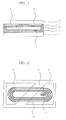
- 1 means a substrate sheet
- 2 means a first adhesive layer
- 3 means an electronic circuit
- 4 means a second adhesive layer
- 5 means an IC chip
- 6 means a release agent layer
- 7 means a release liner.
- FIG. 1 shows an outline of a cross-section of an IC tag of one embodiment of the invention.
- the substrate sheet 1 is preferably a sheet composed of a thermoplastic resin.
- the sheets composed of the thermoplastic resin for example, the sheets composed of one or more of various synthetic resins, such as polyolefin resin like polyethylene resins of high density polyethylene, middle density polyethylene, low density polyethylene and the like, polypropylene resins of polypropylene, polymethyl-1-pentene/ethylene/cyclic olefin copolymer, and ethylene-vinyl acetate copolymer; polyester resins like polyethylene terephthalate, polyethylene naphthalate, polybutylene terephthalate; polyvinyl chloride resins; polyvinylalcohol resins; polycarbonate resins; polyamide resins; polyimide resins; fluororesins; copolymers containing two or more polymerization units thereof; polymer blends containing two or more resins thereof; polymer alloys containing one or more resins thereof can be used.
- various synthetic resins such as polyolefin resin like polyethylene resins of high density polyethylene, middle density polyethylene, low density poly
- the sheets composed of polyester resins are preferably used.
- the substrate sheet 1 may be oriented uniaxially or biaxially.
- the substrate sheet 1 may be composed of single layer or two or more layers of different layers or same layers.
- the substrate sheet 1 has preferably water resistance. If the substrate sheet has water resistance, a damage such as breaking of the substrate sheet is not caused when the substrate sheet is wet with water.
- Thickness of the substrate sheet 1 does not have any limitation. However, the thickness is generally in the range of 10 to 250 ⁇ m and preferably in the range of 20 to 100 ⁇ m.
- the surface of the substrate sheet 1 can be surface-treated.
- the surface-treatment includes, for example, corona discharge treatment, chemical treatment, resin-coating and the like.
- Adhesives used in the first adhesive layer 2 include various adhesives such as thermo melting adhesives, pressure-sensitive adhesives and thermosetting adhesives.
- the kinds of the adhesive include, for example, natural rubber adhesives, synthetic rubber adhesives, acrylic resin adhesives, polyester resin adhesives, polyvinyl ether resin adhesives, urethane resin adhesives and silicone resin adhesives.
- Examples of the synthetic rubber adhesives include styrene-butadiene rubber, polyisobutylene rubber, isobutylene-isoprene rubber, isoprene rubber, styrene-isoprene block copolymer, styrene-butadiene block copolymer, styrene-ethylene-butylene block copolymer, ethylene-vinyl acetate thermoplastic elastomer and the like.
- acrylic resin adhesives examples include homopolymers of monomer such as acrylic acid, methyl acrylate, ethyl acrylate, propyl acrylate, butyl acrylate, 2-ethylhexyl acrylate, methyl methacrylate, ethyl methacrylate, butyl methacrylate, and acrylonitrile, or copolymers of 2 or more of monomers thereof.
- Polyester resin adhesives are copolymers of a polyol and a polybasic acid.
- the polyol includes ethylene glycol, propylene glycol, and butanediol.
- the polybasic acid includes terephthalic acid, adipic acid, and maleic acid.
- polyvinyl ether resin adhesives examples include polyvinyl ether, and polyvinyl isobutyl ether.
- silicone resin adhesives include dimethyl polysiloxane. The adhesives can be used singly or in combination of two or more members.
- the polyester resin adhesives are preferable.
- a tackifier, a softener, an antioxidant, a filler, a coloring agent such as a dye and a pigment or the like can be mixed in the first adhesive layer 2, according to needs.
- the tackifier includes rosin resins, terpene phenol resins, terpene resins, aromatic hydrocarbon modif ied terpene resins, petroleum resins, coumarone-indene resins, styrene resins, phenol resins and xylene resins.
- the softener includes process oils, liquid rubbers and plasticizers.
- the filler includes silica, talc, clay, calcium carbonate and the like.
- Thickness of the first adhesive layer 2 does not have any limitation. However, the thickness is generally in the range of 3 to 100 ⁇ m and preferably in the range of 5 to 50 ⁇ m.
- the release agent layer 6 is formed at positions corresponding to the both ends of the electronic circuit 3 and located at the interface between the substrate sheet 1 and the first adhesive layer 2.
- the release agent layer 6 is formed at positions corresponding to the both ends of the electronic circuit 3 , but is not formed at positions corresponding to the center section of the electronic circuit 3.
- the first adhesive layer 2 is laminated directly on the surface of the substrate sheet 1 at positions corresponding to the center section of the electronic circuit 3. Therefore, when the IC tag is peeled off after the IC tag is attached to the article, the center section of the electronic circuit 3 is peeled off together with the substrate sheet 1 in the state that the center section of the electronic circuit 3 is attached to the first adhesive layer 2, and then the electronic circuit 3 is cut.
- the release agent layer 6 is not needed to cover all of positions corresponding to the both ends of the electronic circuit 3. Accordingly, there may be a section at which the release agent layer 6 is not covered.
- the release agent layer 6 is formed to cover the range of preferably 20 to 90 percents, more preferably 40 to 80 percents of an area surrounded by an outside circumference of the electronic circuit 3 through the first adhesive layer 2.
- the release agent layer 6 is preferably formed as the release agent layer 6 projects over the outside circumference of the electronic circuit 3.
- the width of the projecting area of the release agent layer 6 does not have any limitation. However, the width is preferably in the range of not less than 1 mm.
- the shape of the release agent layer 6 needs the shape capable to form at positions corresponding to the both ends of the electronic circuit 3.
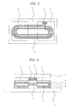
- the shape of the release agent layer 6 includes preferably triangle, quadrangle, polygons such as pentagon and polygons having more than five angles, ellipse and circle (referred to FIG.2 and FIG.3). Two shapes of the release agent layer 6 may be same or different. Two of the release agent layer 6 are preferably separated perfectly and individually, but may be connected at a part of the release agent layer 6.
- Release agents used in the release agent layer 6 include, for example, silicone resin, long chain alkyl group-containing resin and fluororesin.
- Thickness of the release agent layer 6 does not have any limitation. However, the thickness is preferably in the range of 0.01 to 5 ⁇ m and more preferably in the range of 0.03 to 1 ⁇ m.
- the electronic circuit 3 is formed on a surface of the first adhesive layer 2.
- the electronic circuit 3 is a circuit composed of a conductive material.
- the conductive material includes, for example, metal simple substance such as metallic foil, vapor deposition film and thin film produced by spattering.
- metal simple substance gold, silver, nickel, copper, aluminium and the like can be used.
- conductive pastes produced by dispersing a perticle of metal such as gold, silver, nickel and copper in a binder, can be used.
- the average particle diameter of the metal particle is preferably in the range of 1 to 15 ⁇ m and more preferably in the range of 2 to 10 ⁇ m.
- the binder includes, for example, polyester resins, polyurethane resins, epoxy resins and phenol resins.
- Thickness of the layer of conductive material forming the electronic circuit does not have any limitation.
- the thickness of the metallic foil is preferably in the range of 5 to 50 ⁇ m
- the thickness of the vapor deposition film or metallic film produced by spattering is preferably in the range of 0.01 to 1 ⁇ m
- the thickness of conductive paste is preferably in the range of 5 to 30 ⁇ m.
- the method for forming the electronic circuit 3 on the surface of the first adhesive layer 2 include, for example, a method for forming the electronic circuit 3 by adhering a metallic foil to the substrate sheet 1 with adhesive, etching-treating the metallic foil and then removing sections other than the electronic circuit.
- the etching-treatment can be conducted by the same treatment as general etching-treatment.
- the forming of the electronic circuit 3 to the surface of the first adhesive layer 2 can be also conducted by adhering the conductive paste in the shape of the electronic circuit 3 to the surface of the first adhesive layer 2 by means such as printing and application.
- the shape of the electronic circuit 3 includes, for example, shapes indicated by FIG.2 and FIG.3.
- the electronic circuit 3 as an antenna is formed by arranging a line of conductive material in quartet ring having specific space between each lines in the direction from the outside circumference of a rectangle substrate sheet 1 to the inside.
- the electronic circuit 3 may be arranged in quartet ring as indicated in FIG.2 and FIG.3, or may be arranged in singlet ring, doublet ring, triplet ring, or quintet or more ring.
- the length of the electronic circuit 3 can be preferably controlled in a multiple of the wavelength of the received electric wave.
- the IC chip 5 is connected to both ends of the electronic circuit 3.
- the IC chip 5 can be formed inside of the electronic circuit 3, outside of the electronic circuit 3, or in the upper portion of the electronic circuit 3.
- the end of most outside ring or most inside ring of the electronic circuit 3 is preferably connected to the IC chip 5 by forming the line (jumper circuit) from the end over the ring electronic circuit 3 in direction of the inside or the outside of the electronic circuit 3, without short circuit to the ring electronic circuit 3.
- the method for forming the jumper circuit includes a method for forming a conductive circuit line by printing insulating ink in line crossing the portion of the ring electronic circuit 3 from the end of the electronic circuit 3 by screen printing or the like, and then printing conductive paste in line on the printed insulating ink by screen printing or the like.
- the conductive paste includes that described before.
- the insulating ink includes light curable ink such as ultraviolet curable ink.
- the method for connecting the IC chip 5 to the end of the electronic circuit 3 includes a method for connecting by forming an anisotropic conductive film on the surface of the end of the electronic circuit 3 and then connecting flip-chip bonding method via the anisotropic conductive film.
- the flip-chip bonding method is a method for conducting easily between the end of the electronic circuit 3 and the IC chip 5 by forming a wire bump to an electrode portion of the IC chip 5, and pressing the surface of the wire bump formed on the IC chip 5 to the anisotropic conductive film covered on the surface of the end of the electronic circuit 3 so that the wire bump insert in the anisotropic conductive film.
- the second adhesive layer 4 is laminated to cover the electronic circuit 3, the IC chip 5 and the surface of the first adhesive layer 2 that the electronic circuit 3 is not formed.
- Adhesives used in the second adhesive layer 4 include various adhesives such as thermo melting adhesives, pressure-sensitive adhesives and thermosetting adhesives.
- the kinds of the adhesive include, for example, the same as adhesives used in the first adhesive layer 2, as described before.
- the adhesives can be used singly or in combination of two or more members.
- the pressure-sensitive adhesives are preferable and acrylic pressure-sensitive adhesives are more preferable.
- the surface of the second adhesive layer 4 is preferably flat.
- Thickness of the second adhesive layer 4 does not have any limitation. However, the thickness of the portion covering the electronic circuit 3 and the IC chip 5 is different from the thickness of the portion covering the first adhesive layer 2. Maximum thickness is normally in the range of 10 to 100 ⁇ m and preferably in the range of 15 to 50 ⁇ m.
- the surface of the second adhesive layer 4 can be covered with the release liner 7.
- any release liners can be used.
- release liners in which release treatment is conducted to the surface of the substrate to be contacted to the second adhesive layer 4 according to needs, can be used.
- the substrate films composed of various resins such as polyethylene terephthalate, polybutylene terephthalate, polyethylene, polypropylene and polyarylate, and various paper materials such as papers laminated with polyethylene, papers laminated with polypropylene, clay-coated papers, resin-coated papers and glassine papers are illustrated.
- representative examples include a formation of release agent layer composed of release agent such as silicone resin, long-chain alkyl group-containing resin and fluororesin.
- the thickness of the release liner 7 does not have any limitation. However, the thickness can be decided properly.
- the second adhesive layer 4 can be formed by applying directly to the electronic circuit 3, the IC chip 5 and the surface of the first adhesive layer 2 in which the electronic circuit 3 is not formed. Further, after the second adhesive layer is formed by applying the adhesive on the surface of the release agent layer of the release liner 7, the second adhesive layer can be attached to the electronic circuit 3, the IC chip 5 and the surface of the first adhesive layer 2 in which the electronic circuit 3 is not formed.
- Methods for forming the first adhesive layer 3, the second adhesive layer 4 and the release agent layer 6 do not have any limitation, and various methods can be used.
- the methods include, for example, air knife coater, brad coater, bar coater, gravure coater, roll coater, curtain coater, die coater, knife coater, screen coater, Mayer bar coater and kiss coater.
- the substrate sheet 1 is peeled off at the interface against the release agent layer 6 formed to cover the electronic circuit 3, and the substrate sheet 1 without the release agent layer 6 at the center section of the electronic circuit 3 is peeled off at the interface between the article and the second adhesive layer 4 in the state that the second adhesive layer 4, the electronic circuit 3 and the first adhesive layer 2 are attached to the substrate sheet 1, as indicated in FIG. 4. As the result, the electronic circuit 3 is cut.
- the end portion of the substrate sheet 1 When the end portion of the substrate sheet 1 is attached directly to the first adhesive layer 2, the end portion of the substrate sheet 1 may be peeled off at the interface of the substrate sheet 1 and the first adhesive layer 2, or may be peeled off in the layer of the first adhesive layer 2.
- the width of the first adhesive layer 2 attached directly to the end portion of the substrate sheet 1 is short, it is preferable because the substrate sheet 1 is peeled off easily at the interface between the substrate sheet 1 and the first adhesive layer 2.
- a release agent layer 6 was formed by applying a silincone resin release agent in the shape as indicated in FIG. 2 (having angle of the oblique line in trapezoid of 45° , width of unapplied portion of 3 mm, area covered with two trapezoids and surrounded by an outside circumference of the electronic circuit of about 75 percents of area surrounded by an outside circumference of the electronic circuit, and space length between the end of trapezoid and the substrate sheet 1 of 1 mm), on one surface of polyethylene terephthalate film ( having width of 28 mm, length of 12 mm and thickness of 50 ⁇ m) in an amount to form the dried thickness of 0.05 ⁇ m and then curing at 130 °C for 1 minutes.
- a silincone resin release agent in the shape as indicated in FIG. 2 (having angle of the oblique line in trapezoid of 45° , width of unapplied portion of 3 mm, area covered with two trapezoids and surrounded by an outside circumference of the
- polyester type thermo melting adhesive (produced by TOYO BOSEKI CO., LTD. , trade name "BAYRON 30SS”) was applied on the surface of the release agent layer 6 and the substrate sheet 1 by gravure coater in amount to form the dried thickness of 5 ⁇ m to laminate the first adhesive layer 2. Further, on the surface of the first adhesive layer 2, an electrolytic copper foil having thickness of 35 ⁇ m was heated and pressed by heat seal roll of 100°C. Next, on the surface of the electrolytic copper foil, etching resist ink was printed in quintet ring electronic circuit (antenna) having long side of 25 mm, short side of 6 mm and line width of 0.3 mm by screen-printing method, as indicated in FIG.2. The printed electrolytic copper foil was etching-treated with a solution of ferric chloride to remove the portion other than the circuit. And then, the etching resist ink was removed with an aqueous alkali solution to form the electronic circuit 3.
- an ultraviolet curable ink was printed to the space between them in line shape by screen printing method. And then, ultraviolet light was irradiated to cure the ultraviolet curable ink. Next, a silver paste (average particle diameter of silver particle of 5 ⁇ m, binder of polyester resin) was printed in line shape (having length of 10 mm) on the surface of the cured line of the ultraviolet curable ink, and dried to form the jumper circuit.
- a wire bump was formed at the electrode portion of an IC chip 5 (produced by PHILIPS CO., trade name of " I /CODE” ) with a gold wire.
- the IC chip 5 was connected to the both ends of the circuit through an anisotropic conductive film (produced by SONY CHIMICAL CO., LTD., trade name of "FP2322D”) by using the flip chip bonding method.
- a release paper having the second adhesive layer 4 was prepared by applying an acrylic pressure-sensitive adhesive having low adhesive strength (produced by LINTEC CORPORATION, trade name of "PA-T1") on the release-treated surface of the release paper obtained by release-treating all surface of one side of a glassine paper having thickness of 70 ⁇ m with silicone resin by using roll knife coater, and drying to form the second adhesive layer 4 having thickness of 20 ⁇ m.
- an acrylic pressure-sensitive adhesive having low adhesive strength produced by LINTEC CORPORATION, trade name of "PA-T1"
- the second adhesive layer 4 in the release paper with the second adhesive layer 4 was covered on the first adhesive layer 2, the electronic circuit 3 and the IC chip 5 to prepare the IC tag.
- the obtained IC tag was tested by non-contact transmitting and receiving test. At the result, the transmitting and receiving could be conducted correctly.
- the all surface-treated release paper in the IC tag was peeled off, and the IC tag was attached to a polypropylene resin plate. After 24 hours, the IC tag was peeled off from the polypropylene resin plate. The portion of the electronic circuit 3 covered with the release agent layer 6 was remained on the polypropylene resin plate. The portion other than the release agent layer 6 was peeled off from the polypropylene resin plate together with the polyethylene terephthalate sheet of the substrate sheet 1. According to the peeling, the electronic circuit 3 was cut. The peeled IC tag was tested by non-contact transmitting and receiving test. At the result, the transmitting and receiving could be not conducted.
- the IC tag were prepared in the same method as described in Example 1 except that the release agent layer 6 was not formed.
- the obtained IC tag was tested by non-contact transmitting and receiving test. At the result, the transmitting and receiving could be conducted correctly.
- the IC tag was attached to the polypropylene resin plate and peeled off in the same method as described in Example 1.
- the IC tag could be peeled off easily and the electronic circuit 3 was not broken.
- the peeled IC tag was tested by non-contact transmitting and receiving test. At the result, the transmitting and receiving could be conducted correctly.
- the built-in electronic circuit can be surely broken.
Landscapes
- Engineering & Computer Science (AREA)
- Computer Hardware Design (AREA)
- Microelectronics & Electronic Packaging (AREA)
- Physics & Mathematics (AREA)
- General Physics & Mathematics (AREA)
- Theoretical Computer Science (AREA)
- Computer Security & Cryptography (AREA)
- General Engineering & Computer Science (AREA)
- Credit Cards Or The Like (AREA)
- Adhesives Or Adhesive Processes (AREA)
Abstract
Description
The printed electrolytic copper foil was etching-treated with a solution of ferric chloride to remove the portion other than the circuit. And then, the etching resist ink was removed with an aqueous alkali solution to form the
Claims (3)
- An IC tag which has a structure comprising a first adhesive layer laminated on a surface of a substrate sheet, an electronic circuit and an IC chip connecting both ends of the electronic circuit, both the electronic circuit and the IC chip being formed on a surface of the first adhesive layer, and a second adhesive layer laminated for covering the electronic circuit and the IC chip, wherein a release agent layer is further formed at positions corresponding to the both ends of the electronic circuit and located at the interface between the substrate sheet and the first adhesive layer.
- The IC tag as claimed in claim 1, wherein the release agent layer is formed to cover the range of 20 to 90 percents of an area surrounded by an outside circumference of the electronic circuit through the first adhesive layer.
- The IC tag as claimed in claim 1 or claim 2, wherein a release liner is formed on a surface of the second adhesive layer.
Applications Claiming Priority (3)
| Application Number | Priority Date | Filing Date | Title |
|---|---|---|---|
| JP2002140535 | 2002-05-15 | ||
| JP2002140535A JP4342771B2 (en) | 2002-05-15 | 2002-05-15 | IC tag |
| PCT/JP2003/006026 WO2003098545A1 (en) | 2002-05-15 | 2003-05-14 | Ic tag |
Publications (3)
| Publication Number | Publication Date |
|---|---|
| EP1505537A1 true EP1505537A1 (en) | 2005-02-09 |
| EP1505537A4 EP1505537A4 (en) | 2005-09-14 |
| EP1505537B1 EP1505537B1 (en) | 2006-11-22 |
Family
ID=29544927
Family Applications (1)
| Application Number | Title | Priority Date | Filing Date |
|---|---|---|---|
| EP03741114A Expired - Lifetime EP1505537B1 (en) | 2002-05-15 | 2003-05-14 | Ic tag |
Country Status (8)
| Country | Link |
|---|---|
| US (1) | US7540427B2 (en) |
| EP (1) | EP1505537B1 (en) |
| JP (1) | JP4342771B2 (en) |
| KR (1) | KR100921863B1 (en) |
| CN (1) | CN1653485A (en) |
| DE (1) | DE60309860T2 (en) |
| TW (1) | TWI329282B (en) |
| WO (1) | WO2003098545A1 (en) |
Cited By (4)
| Publication number | Priority date | Publication date | Assignee | Title |
|---|---|---|---|---|
| WO2008067830A1 (en) * | 2006-12-05 | 2008-06-12 | Hueck Folien Ges.M.B.H. | Manipulation-proof rfid antenna |
| US7633145B2 (en) | 2004-01-16 | 2009-12-15 | Semiconductor Energy Laboratory Co., Ltd. | Semiconductor device with antenna and separating layer |
| WO2011092144A1 (en) * | 2010-01-26 | 2011-08-04 | Schreiner Group Gmbh & Co. Kg | Security tag, assembly having a security tag and method for operating a security tag |
| EP1845482A3 (en) * | 2006-04-13 | 2012-10-24 | Brother Kogyo Kabushiki Kaisha | Tag tape and RFID label |
Families Citing this family (19)
| Publication number | Priority date | Publication date | Assignee | Title |
|---|---|---|---|---|
| JP4800204B2 (en) * | 2004-02-27 | 2011-10-26 | 日本カーバイド工業株式会社 | Display device having anti-theft structure |
| JP4529486B2 (en) * | 2004-03-04 | 2010-08-25 | 凸版印刷株式会社 | Non-contact IC media |
| JP4354317B2 (en) * | 2004-03-25 | 2009-10-28 | リンテック株式会社 | IC tag and manufacturing method thereof |
| JP4590908B2 (en) * | 2004-04-09 | 2010-12-01 | 凸版印刷株式会社 | Non-contact IC medium and method of manufacturing non-contact IC medium |
| WO2005104026A1 (en) * | 2004-04-23 | 2005-11-03 | Konica Minolta Photo Imaging, Inc. | Ic card and method of producing the same |
| JP4549765B2 (en) * | 2004-07-22 | 2010-09-22 | 大日本印刷株式会社 | Non-contact data carrier with break detection function |
| JP4675184B2 (en) * | 2004-10-29 | 2011-04-20 | リンテック株式会社 | IC tag |
| JP2006134249A (en) * | 2004-11-09 | 2006-05-25 | Fujitsu Ltd | RFID tag |
| JP2006324075A (en) * | 2005-05-18 | 2006-11-30 | Matsushita Electric Ind Co Ltd | Battery pack |
| BRPI0710244B1 (en) * | 2006-04-10 | 2022-02-08 | Innovatier, Inc | ELECTRONIC INLAY AND ELECTRONIC CARD AND METHODS TO MANUFACTURE THEM |
| JP2009075712A (en) * | 2007-09-19 | 2009-04-09 | Toppan Printing Co Ltd | IC label for forgery prevention |
| EP2278662A4 (en) * | 2008-04-24 | 2015-05-27 | Toray Industries | Non-contact ic tag |
| EP2164032B1 (en) * | 2008-09-15 | 2018-07-18 | Hueck Folien Ges.m.b.H. | Manipulation-proof RFID antenna with safety feature |
| JP5220654B2 (en) * | 2009-02-24 | 2013-06-26 | 富士通株式会社 | RFID tag |
| JP6073048B2 (en) * | 2011-07-04 | 2017-02-01 | 東洋アルミニウム株式会社 | RFID inlet antenna and RFID using the same |
| CN103971590B (en) * | 2013-02-01 | 2017-02-22 | 比亚迪股份有限公司 | Anti-counterfeiting trademark and manufacturing method thereof |
| JP2015060504A (en) * | 2013-09-20 | 2015-03-30 | 凸版印刷株式会社 | Non-contact ic label |
| JP6673022B2 (en) | 2016-05-31 | 2020-03-25 | 富士通株式会社 | Electronic devices and beacons |
| JP7767744B2 (en) * | 2021-06-17 | 2025-11-12 | Toppanホールディングス株式会社 | packaging material |
Family Cites Families (21)
| Publication number | Priority date | Publication date | Assignee | Title |
|---|---|---|---|---|
| US4717438A (en) * | 1986-09-29 | 1988-01-05 | Monarch Marking Systems, Inc. | Method of making tags |
| US5108819A (en) * | 1990-02-14 | 1992-04-28 | Eli Lilly And Company | Thin film electrical component |
| US5131686A (en) * | 1990-09-20 | 1992-07-21 | Carlson Thomas S | Method for producing identification cards |
| US5142270A (en) * | 1991-05-22 | 1992-08-25 | Checkpoint Systems Inc. | Stabilized resonant tag circuit and deactivator |
| US5767772A (en) * | 1993-12-15 | 1998-06-16 | Lemaire; Gerard | Marker for an article which is detected when it passes through a surveillance zone |
| US5528222A (en) * | 1994-09-09 | 1996-06-18 | International Business Machines Corporation | Radio frequency circuit and memory in thin flexible package |
| US6270871B1 (en) * | 1996-09-27 | 2001-08-07 | Avery Dennison Corporation | Overlaminated pressure-sensitive adhesive construction |
| US5884425A (en) * | 1997-05-23 | 1999-03-23 | Avery Dennison Corporation | Anti-tamper tag with theft protection |
| JP3853480B2 (en) * | 1997-09-05 | 2006-12-06 | 大日本印刷株式会社 | Non-contact IC card |
| JP4046167B2 (en) * | 1998-08-12 | 2008-02-13 | リンテック株式会社 | Non-contact data carrier label |
| JP2000105806A (en) * | 1998-09-29 | 2000-04-11 | Toshiba Chem Corp | Label type noncontact data carrier |
| US6147604A (en) * | 1998-10-15 | 2000-11-14 | Intermec Ip Corporation | Wireless memory device |
| US6262692B1 (en) * | 1999-01-13 | 2001-07-17 | Brady Worldwide, Inc. | Laminate RFID label and method of manufacture |
| JP4095741B2 (en) * | 1999-06-29 | 2008-06-04 | シチズンミヨタ株式会社 | IC tag structure |
| JP4117989B2 (en) | 1999-12-10 | 2008-07-16 | シチズンミヨタ株式会社 | IC tag |
| JP3557981B2 (en) * | 2000-01-17 | 2004-08-25 | ソニーケミカル株式会社 | Information recording tag |
| US6888509B2 (en) * | 2000-03-21 | 2005-05-03 | Mikoh Corporation | Tamper indicating radio frequency identification label |
| US7049962B2 (en) * | 2000-07-28 | 2006-05-23 | Micoh Corporation | Materials and construction for a tamper indicating radio frequency identification label |
| JP2002222403A (en) * | 2001-01-25 | 2002-08-09 | Konica Corp | Ic-mounted card base material, ic-mounted individual identifying card and its manufacturing method |
| US6830193B2 (en) * | 2001-11-29 | 2004-12-14 | Matsushita Electric Industrial Co., Ltd. | Non-contact IC card |
| JP2003302907A (en) * | 2002-04-12 | 2003-10-24 | Matsushita Electric Ind Co Ltd | sticker |
-
2002
- 2002-05-15 JP JP2002140535A patent/JP4342771B2/en not_active Expired - Fee Related
-
2003
- 2003-05-14 KR KR1020047018113A patent/KR100921863B1/en not_active Expired - Fee Related
- 2003-05-14 US US10/514,495 patent/US7540427B2/en not_active Expired - Fee Related
- 2003-05-14 WO PCT/JP2003/006026 patent/WO2003098545A1/en not_active Ceased
- 2003-05-14 EP EP03741114A patent/EP1505537B1/en not_active Expired - Lifetime
- 2003-05-14 DE DE60309860T patent/DE60309860T2/en not_active Expired - Lifetime
- 2003-05-14 CN CNA038110164A patent/CN1653485A/en active Pending
- 2003-05-14 TW TW092113061A patent/TWI329282B/en not_active IP Right Cessation
Cited By (4)
| Publication number | Priority date | Publication date | Assignee | Title |
|---|---|---|---|---|
| US7633145B2 (en) | 2004-01-16 | 2009-12-15 | Semiconductor Energy Laboratory Co., Ltd. | Semiconductor device with antenna and separating layer |
| EP1845482A3 (en) * | 2006-04-13 | 2012-10-24 | Brother Kogyo Kabushiki Kaisha | Tag tape and RFID label |
| WO2008067830A1 (en) * | 2006-12-05 | 2008-06-12 | Hueck Folien Ges.M.B.H. | Manipulation-proof rfid antenna |
| WO2011092144A1 (en) * | 2010-01-26 | 2011-08-04 | Schreiner Group Gmbh & Co. Kg | Security tag, assembly having a security tag and method for operating a security tag |
Also Published As
| Publication number | Publication date |
|---|---|
| TWI329282B (en) | 2010-08-21 |
| EP1505537B1 (en) | 2006-11-22 |
| CN1653485A (en) | 2005-08-10 |
| EP1505537A4 (en) | 2005-09-14 |
| WO2003098545A1 (en) | 2003-11-27 |
| JP2003331248A (en) | 2003-11-21 |
| DE60309860T2 (en) | 2007-09-13 |
| TW200407810A (en) | 2004-05-16 |
| KR20040104727A (en) | 2004-12-10 |
| JP4342771B2 (en) | 2009-10-14 |
| US7540427B2 (en) | 2009-06-02 |
| DE60309860D1 (en) | 2007-01-04 |
| KR100921863B1 (en) | 2009-10-13 |
| US20060273179A1 (en) | 2006-12-07 |
Similar Documents
| Publication | Publication Date | Title |
|---|---|---|
| US7540427B2 (en) | IC tag | |
| US9048525B2 (en) | Antenna circuit | |
| US7294917B2 (en) | IC tag | |
| WO2008047705A1 (en) | Ic tag label | |
| US8292188B2 (en) | Electronic circuit and IC tag | |
| CN108510042B (en) | Fragile electronic tag | |
| JP4127650B2 (en) | IC tag | |
| JP3956660B2 (en) | Non-contact type IC tag and method for manufacturing non-contact type IC tag | |
| JP2003167515A (en) | Rfid tag for managing ink cartridge and ink cartridge attached with the same | |
| CN100367308C (en) | IC label | |
| US20250322771A1 (en) | Rfid label for medical device | |
| JP5806062B2 (en) | Non-contact data transmitter / receiver | |
| JP4339069B2 (en) | IC tag | |
| JP4354317B2 (en) | IC tag and manufacturing method thereof | |
| EP1653506A1 (en) | Flip chip mounting substrate | |
| JP2018036417A (en) | Transfer-type security label sheet, method for attaching security label, and security label | |
| CN208766697U (en) | A kind of frangible electronic tag | |
| CN206863791U (en) | A kind of frangible label of anti-alice | |
| JP2004317544A (en) | Label with IC chip mount | |
| JP2008077127A (en) | IC tag connecting body | |
| JP2007004535A (en) | IC inlet and IC tag | |
| JP2007004818A (en) | Non-contact ic tag and method for manufacturing non-contact ic tag |
Legal Events
| Date | Code | Title | Description |
|---|---|---|---|
| PUAI | Public reference made under article 153(3) epc to a published international application that has entered the european phase |
Free format text: ORIGINAL CODE: 0009012 |
|
| 17P | Request for examination filed |
Effective date: 20041110 |
|
| AK | Designated contracting states |
Kind code of ref document: A1 Designated state(s): AT BE BG CH CY CZ DE DK EE ES FI FR GB GR HU IE IT LI LU MC NL PT RO SE SI SK TR |
|
| RBV | Designated contracting states (corrected) |
Designated state(s): DE FR GB |
|
| A4 | Supplementary search report drawn up and despatched |
Effective date: 20050728 |
|
| GRAP | Despatch of communication of intention to grant a patent |
Free format text: ORIGINAL CODE: EPIDOSNIGR1 |
|
| GRAS | Grant fee paid |
Free format text: ORIGINAL CODE: EPIDOSNIGR3 |
|
| GRAA | (expected) grant |
Free format text: ORIGINAL CODE: 0009210 |
|
| AK | Designated contracting states |
Kind code of ref document: B1 Designated state(s): DE FR GB |
|
| REG | Reference to a national code |
Ref country code: GB Ref legal event code: FG4D |
|
| REF | Corresponds to: |
Ref document number: 60309860 Country of ref document: DE Date of ref document: 20070104 Kind code of ref document: P |
|
| ET | Fr: translation filed | ||
| PLBE | No opposition filed within time limit |
Free format text: ORIGINAL CODE: 0009261 |
|
| STAA | Information on the status of an ep patent application or granted ep patent |
Free format text: STATUS: NO OPPOSITION FILED WITHIN TIME LIMIT |
|
| 26N | No opposition filed |
Effective date: 20070823 |
|
| PGFP | Annual fee paid to national office [announced via postgrant information from national office to epo] |
Ref country code: GB Payment date: 20100329 Year of fee payment: 8 |
|
| PGFP | Annual fee paid to national office [announced via postgrant information from national office to epo] |
Ref country code: FR Payment date: 20100525 Year of fee payment: 8 |
|
| PGFP | Annual fee paid to national office [announced via postgrant information from national office to epo] |
Ref country code: DE Payment date: 20100512 Year of fee payment: 8 |
|
| GBPC | Gb: european patent ceased through non-payment of renewal fee |
Effective date: 20110514 |
|
| REG | Reference to a national code |
Ref country code: FR Ref legal event code: ST Effective date: 20120131 |
|
| REG | Reference to a national code |
Ref country code: DE Ref legal event code: R119 Ref document number: 60309860 Country of ref document: DE Effective date: 20111201 |
|
| PG25 | Lapsed in a contracting state [announced via postgrant information from national office to epo] |
Ref country code: FR Free format text: LAPSE BECAUSE OF NON-PAYMENT OF DUE FEES Effective date: 20110531 |
|
| PG25 | Lapsed in a contracting state [announced via postgrant information from national office to epo] |
Ref country code: GB Free format text: LAPSE BECAUSE OF NON-PAYMENT OF DUE FEES Effective date: 20110514 |
|
| PG25 | Lapsed in a contracting state [announced via postgrant information from national office to epo] |
Ref country code: DE Free format text: LAPSE BECAUSE OF NON-PAYMENT OF DUE FEES Effective date: 20111201 |