EP1498787A2 - Bilderzeugungsgerät und elastische Halbleiterolle zum Übertragen von Tonerbildern - Google Patents
Bilderzeugungsgerät und elastische Halbleiterolle zum Übertragen von Tonerbildern Download PDFInfo
- Publication number
- EP1498787A2 EP1498787A2 EP04253620A EP04253620A EP1498787A2 EP 1498787 A2 EP1498787 A2 EP 1498787A2 EP 04253620 A EP04253620 A EP 04253620A EP 04253620 A EP04253620 A EP 04253620A EP 1498787 A2 EP1498787 A2 EP 1498787A2
- Authority
- EP
- European Patent Office
- Prior art keywords
- voltage
- transfer
- resistance value
- image
- image forming
- Prior art date
- Legal status (The legal status is an assumption and is not a legal conclusion. Google has not performed a legal analysis and makes no representation as to the accuracy of the status listed.)
- Granted
Links
- 238000012546 transfer Methods 0.000 claims abstract description 233
- 239000000463 material Substances 0.000 claims abstract description 59
- 229910052751 metal Inorganic materials 0.000 claims description 13
- 239000002184 metal Substances 0.000 claims description 13
- 239000006229 carbon black Substances 0.000 claims description 11
- PXHVJJICTQNCMI-UHFFFAOYSA-N Nickel Chemical compound [Ni] PXHVJJICTQNCMI-UHFFFAOYSA-N 0.000 claims description 10
- 239000002245 particle Substances 0.000 claims description 10
- RYGMFSIKBFXOCR-UHFFFAOYSA-N Copper Chemical compound [Cu] RYGMFSIKBFXOCR-UHFFFAOYSA-N 0.000 claims description 5
- BQCADISMDOOEFD-UHFFFAOYSA-N Silver Chemical compound [Ag] BQCADISMDOOEFD-UHFFFAOYSA-N 0.000 claims description 5
- 229910052783 alkali metal Inorganic materials 0.000 claims description 5
- -1 alkali metal salt Chemical class 0.000 claims description 5
- 229910052802 copper Inorganic materials 0.000 claims description 5
- 239000010949 copper Substances 0.000 claims description 5
- 239000000835 fiber Substances 0.000 claims description 5
- 229910052759 nickel Inorganic materials 0.000 claims description 5
- 229910052709 silver Inorganic materials 0.000 claims description 5
- 239000004332 silver Substances 0.000 claims description 5
- OKTJSMMVPCPJKN-UHFFFAOYSA-N Carbon Chemical compound [C] OKTJSMMVPCPJKN-UHFFFAOYSA-N 0.000 claims description 4
- 229910052799 carbon Inorganic materials 0.000 claims description 4
- 239000010410 layer Substances 0.000 description 27
- 150000002500 ions Chemical class 0.000 description 26
- 238000007639 printing Methods 0.000 description 26
- KFZMGEQAYNKOFK-UHFFFAOYSA-N Isopropanol Chemical compound CC(C)O KFZMGEQAYNKOFK-UHFFFAOYSA-N 0.000 description 24
- 238000010586 diagram Methods 0.000 description 23
- 238000004073 vulcanization Methods 0.000 description 18
- LYCAIKOWRPUZTN-UHFFFAOYSA-N Ethylene glycol Chemical compound OCCO LYCAIKOWRPUZTN-UHFFFAOYSA-N 0.000 description 15
- 229920001296 polysiloxane Polymers 0.000 description 15
- 239000002585 base Substances 0.000 description 14
- 239000004020 conductor Substances 0.000 description 12
- XLOMVQKBTHCTTD-UHFFFAOYSA-N Zinc monoxide Chemical compound [Zn]=O XLOMVQKBTHCTTD-UHFFFAOYSA-N 0.000 description 10
- 230000007613 environmental effect Effects 0.000 description 9
- 239000005518 polymer electrolyte Substances 0.000 description 9
- 230000002950 deficient Effects 0.000 description 7
- 238000010438 heat treatment Methods 0.000 description 7
- 239000003795 chemical substances by application Substances 0.000 description 6
- 238000005187 foaming Methods 0.000 description 6
- MHCFAGZWMAWTNR-UHFFFAOYSA-M lithium perchlorate Chemical compound [Li+].[O-]Cl(=O)(=O)=O MHCFAGZWMAWTNR-UHFFFAOYSA-M 0.000 description 6
- 229910001486 lithium perchlorate Inorganic materials 0.000 description 6
- 238000000034 method Methods 0.000 description 6
- GWEVSGVZZGPLCZ-UHFFFAOYSA-N Titan oxide Chemical compound O=[Ti]=O GWEVSGVZZGPLCZ-UHFFFAOYSA-N 0.000 description 5
- 239000011247 coating layer Substances 0.000 description 5
- 150000001875 compounds Chemical class 0.000 description 5
- 229940093476 ethylene glycol Drugs 0.000 description 5
- 238000004519 manufacturing process Methods 0.000 description 5
- 229920002379 silicone rubber Polymers 0.000 description 5
- 239000004945 silicone rubber Substances 0.000 description 5
- OGIDPMRJRNCKJF-UHFFFAOYSA-N titanium oxide Inorganic materials [Ti]=O OGIDPMRJRNCKJF-UHFFFAOYSA-N 0.000 description 5
- XLYOFNOQVPJJNP-UHFFFAOYSA-N water Substances O XLYOFNOQVPJJNP-UHFFFAOYSA-N 0.000 description 5
- 239000011787 zinc oxide Substances 0.000 description 5
- JOYRKODLDBILNP-UHFFFAOYSA-N Ethyl urethane Chemical compound CCOC(N)=O JOYRKODLDBILNP-UHFFFAOYSA-N 0.000 description 4
- 230000007423 decrease Effects 0.000 description 4
- 229920002943 EPDM rubber Polymers 0.000 description 3
- OKKJLVBELUTLKV-UHFFFAOYSA-N Methanol Chemical compound OC OKKJLVBELUTLKV-UHFFFAOYSA-N 0.000 description 3
- 229920000459 Nitrile rubber Polymers 0.000 description 3
- 230000032683 aging Effects 0.000 description 3
- 238000007598 dipping method Methods 0.000 description 3
- 239000011347 resin Substances 0.000 description 3
- 229920005989 resin Polymers 0.000 description 3
- 238000004140 cleaning Methods 0.000 description 2
- 239000000428 dust Substances 0.000 description 2
- 239000003792 electrolyte Substances 0.000 description 2
- 238000009413 insulation Methods 0.000 description 2
- 229920002981 polyvinylidene fluoride Polymers 0.000 description 2
- 238000011144 upstream manufacturing Methods 0.000 description 2
- 239000004677 Nylon Substances 0.000 description 1
- WGKMWBIFNQLOKM-UHFFFAOYSA-N [O].[Cl] Chemical compound [O].[Cl] WGKMWBIFNQLOKM-UHFFFAOYSA-N 0.000 description 1
- 239000002253 acid Substances 0.000 description 1
- 238000004364 calculation method Methods 0.000 description 1
- 238000006243 chemical reaction Methods 0.000 description 1
- 229920001940 conductive polymer Polymers 0.000 description 1
- 238000010276 construction Methods 0.000 description 1
- 230000008878 coupling Effects 0.000 description 1
- 238000010168 coupling process Methods 0.000 description 1
- 238000005859 coupling reaction Methods 0.000 description 1
- 238000011161 development Methods 0.000 description 1
- 230000018109 developmental process Effects 0.000 description 1
- 230000005684 electric field Effects 0.000 description 1
- 238000002474 experimental method Methods 0.000 description 1
- 239000000945 filler Substances 0.000 description 1
- 230000002209 hydrophobic effect Effects 0.000 description 1
- 238000012886 linear function Methods 0.000 description 1
- 229910003002 lithium salt Inorganic materials 0.000 description 1
- 159000000002 lithium salts Chemical class 0.000 description 1
- 238000012986 modification Methods 0.000 description 1
- 230000004048 modification Effects 0.000 description 1
- 229920001778 nylon Polymers 0.000 description 1
- 229920011301 perfluoro alkoxyl alkane Polymers 0.000 description 1
- 230000002093 peripheral effect Effects 0.000 description 1
- 238000005293 physical law Methods 0.000 description 1
- 230000010287 polarization Effects 0.000 description 1
- 229920000642 polymer Polymers 0.000 description 1
- XAEFZNCEHLXOMS-UHFFFAOYSA-M potassium benzoate Chemical compound [K+].[O-]C(=O)C1=CC=CC=C1 XAEFZNCEHLXOMS-UHFFFAOYSA-M 0.000 description 1
- 238000003825 pressing Methods 0.000 description 1
- 230000001737 promoting effect Effects 0.000 description 1
- 150000003839 salts Chemical class 0.000 description 1
- 239000004065 semiconductor Substances 0.000 description 1
- 159000000000 sodium salts Chemical class 0.000 description 1
- 239000000126 substance Substances 0.000 description 1
- 229920001187 thermosetting polymer Polymers 0.000 description 1
- ORGHESHFQPYLAO-UHFFFAOYSA-N vinyl radical Chemical compound C=[CH] ORGHESHFQPYLAO-UHFFFAOYSA-N 0.000 description 1
Images


Classifications
-
- G—PHYSICS
- G03—PHOTOGRAPHY; CINEMATOGRAPHY; ANALOGOUS TECHNIQUES USING WAVES OTHER THAN OPTICAL WAVES; ELECTROGRAPHY; HOLOGRAPHY
- G03G—ELECTROGRAPHY; ELECTROPHOTOGRAPHY; MAGNETOGRAPHY
- G03G15/00—Apparatus for electrographic processes using a charge pattern
- G03G15/14—Apparatus for electrographic processes using a charge pattern for transferring a pattern to a second base
- G03G15/16—Apparatus for electrographic processes using a charge pattern for transferring a pattern to a second base of a toner pattern, e.g. a powder pattern, e.g. magnetic transfer
- G03G15/1665—Apparatus for electrographic processes using a charge pattern for transferring a pattern to a second base of a toner pattern, e.g. a powder pattern, e.g. magnetic transfer by introducing the second base in the nip formed by the recording member and at least one transfer member, e.g. in combination with bias or heat
- G03G15/167—Apparatus for electrographic processes using a charge pattern for transferring a pattern to a second base of a toner pattern, e.g. a powder pattern, e.g. magnetic transfer by introducing the second base in the nip formed by the recording member and at least one transfer member, e.g. in combination with bias or heat at least one of the recording member or the transfer member being rotatable during the transfer
- G03G15/1685—Structure, details of the transfer member, e.g. chemical composition
-
- G—PHYSICS
- G03—PHOTOGRAPHY; CINEMATOGRAPHY; ANALOGOUS TECHNIQUES USING WAVES OTHER THAN OPTICAL WAVES; ELECTROGRAPHY; HOLOGRAPHY
- G03G—ELECTROGRAPHY; ELECTROPHOTOGRAPHY; MAGNETOGRAPHY
- G03G2215/00—Apparatus for electrophotographic processes
- G03G2215/16—Transferring device, details
- G03G2215/1604—Main transfer electrode
- G03G2215/1614—Transfer roll
Definitions
- the invention relates to an image forming apparatus and an elastic roller.
- a surface of a photosensitive drum is uniformly and evenly charged by a charging roller and exposed by an exposing apparatus, an electrostatic latent image is formed onto the surface, the electrostatic latent image is developed by a developing roller, and a toner image is formed.
- the toner image is transferred onto a print medium by a transfer roller, the transferred toner image is fixed by a fixing apparatus, and an image is formed (for example, refer to JP-A-9-212012).
- the transfer of the toner image is executed in a nip portion which is formed between the photosensitive drum and the transfer roller.
- a potential difference is formed between the photosensitive drum and the transfer roller and toner on the photosensitive drum is electrostatically moved onto the print medium by the potential difference. Therefore, to improve image quality, it is important to move just enough toner on the photosensitive drum onto the print medium.
- the toner on the photosensitive drum is moved at a position just before the position on an upstream side of the nip portion in the conveying direction of the print medium and defective printing such as what is called dust printing occurs.
- the potential difference is too small, the transfer is insufficient, the toner remains on the downstream side of the nip portion in the rotating direction of the photosensitive drum, and defective printing such as hazy printing occurs.
- a small potential difference for example, about 1 [kV]
- a current which is generated in association with the applied potential difference is read out.
- a resistance value of the transfer roller is calculated on the basis of the read-out current and fed back, thereby calculating an optimum transfer voltage (for example, 5000 [V]) with reference to a control table which has previously been formed.
- the transfer roller is constructed by an axis made of a metal and an elastic layer formed around the axis. It is ideal that a resistance value between the axis and the surface of the transfer roller is set to a value within a range from 10 7 to 10 9 [ ⁇ ].
- the elastic layer is made of a foaming material using urethane, NBR, EPDM, silicone, or the like as a base material. Since each of the above materials inherently has insulation performance, the semiconductive roller whose resistance value has a proper value is molded by adding an electron conductive material such as carbon black, conductive polymer, metal filler, or the like or an ion conductive material according to an electrolyte into each of the above materials.
- a resistance value depends largely (exponentially) on a transfer voltage, it is constant without depending on the temperature and the humidity.
- a generated transfer current is directly proportional to the transfer voltage (a resistance value is constant without depending on the voltage) and the resistance value depends largely on the temperature and the humidity.
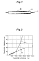
- Fig. 2 is a graph showing a relation between the transfer voltage and the transfer current in the conventional transfer roller.
- Fig. 3 is a graph showing a relation between the transfer voltage and a voltage margin in the conventional transfer roller.
- Fig. 4 is a graph showing a change in resistance value in association with changes in temperature and humidity in the conventional transfer roller.
- an axis of abscissa indicates the transfer voltage which is applied to the transfer roller and an axis of ordinate indicates the transfer current flowing in the transfer roller.
- an axis of abscissa indicates the transfer voltage and an axis of ordinate indicates the voltage margin.
- Fig. 1 is a graph showing a relation between the transfer voltage and the transfer current in the conventional transfer roller.
- Fig. 3 is a graph showing a relation between the transfer voltage and a voltage margin in the conventional transfer roller.
- Fig. 4 is a graph showing a change in resistance value in association with changes in temperature and humidity in the conventional transfer roller.
- an axis of abscissa indicates states of environmental degrees of the temperature and the humidity and an axis of ordinate indicates a ratio of the resistance value at the time when the transfer roller is held in an environment of a high temperature and a high humidity and a ratio of the resistance value at the time when the transfer roller is held in an environment of a low temperature and a low humidity on the assumption that the resistance value which is obtained when the transfer roller is held in an environment of the normal temperature and the normal humidity is set to 1.00.
- L1 denotes a line showing a relation between the transfer voltage and the transfer current in the electron conduction
- L2 indicates a line showing a relation between the transfer voltage and the transfer current in the ion conduction, respectively.
- L3 denotes a line showing a relation between the transfer voltage and the voltage margin in the electron conduction
- L4 indicates a line showing a relation between the transfer voltage and the voltage margin in the ion conduction, respectively.
- the transfer current is expressed by an exponential function of the transfer voltage as shown by the line L1
- the resistance value depends largely on the transfer voltage
- the voltage margin at the time when the transfer voltage is changed changes largely as shown by the line L3.
- the resistance value does not depend on the transfer voltage in the ion conduction. Therefore, the voltage margin at the time when the transfer voltage is changed is almost constant as shown by the line L4.
- the voltage margin shows a change [ ⁇ A/V] in transfer current to the change in transfer voltage.
- the resistance value of the transfer roller has a variation in the circumferential direction, for example, if the current deviated from an average value in the circumferential direction is read at a point when a pre-voltage is applied, the transfer voltage is not optimum and the transfer current which is generated is not optimum, either.
- the transfer current is large, the transfer becomes excessive and, as mentioned above, the toner on the photosensitive drum is moved at a position just before the position on the upstream side of the nip portion in the conveying direction of the print medium and the defective printing such as what is called dust printing occurs.
- the transfer current is small, the transfer is insufficient, the toner remains on the downstream side of the nip portion in the rotating direction of the photosensitive drum, and defective printing such as hazy printing occurs.
- the transfer current is expressed by a linear function of the transfer voltage as shown by the line L2 and the resistance value and an electric conductivity do not depend on the voltage. Therefore, since the transfer current can be precisely controlled better than that in the electron conduction, high picture quality can be realized.
- the ratio of the resistance value when the transfer roller is held in the environment of the low temperature and the low humidity to the resistance value when the transfer roller is held in the environment of the normal temperature and the normal humidity is equal to 2.07 in the case of the electron conduction and is equal to 5.23 in the case of the ion conduction.
- the ratio of the resistance value when the transfer roller is held in the environment of the high temperature and the high humidity to the resistance value when the transfer roller is held in the environment of the normal temperature and the normal humidity is equal to 1.36 in the case of the electron conduction and is equal to 0.10 in the case of the ion conduction, so that the resistance value fluctuates largely in dependence on the temperature and the humidity. In other words, the resistance value decreases in the environment of the high temperature and the high humidity, while the resistance value increases in the environment of the low temperature and the low humidity.
- the transfer voltage according to the resistance value is necessary. Particularly, if the resistance value increases when the transfer roller is held in the environment of the low temperature and the low humidity, it is necessary to raise the transfer voltage.
- an image forming apparatus which forms a developer image by making a developer adhere onto an electrostatic latent image formed on an image holding body, further transfers the developer image onto an image forming medium by using a transferring member, then forms an image, wherein the transferring member has a first resistance value when being added by a voltage of 500 [V] and a second resistance value when being added by a voltage of 1000 [V], the ratio of the second and the first resistance values is between 0.5 and 0.89.
- the transferring member may further have a third resistance value when being added by a voltage of 2000 [V], the ratio of the third and the second resistance values is between 0.3 and 0.88.
- the transferring member may contain a material with electron conductivity.
- the material with electron conductivity includes at least one of carbon black, carbon quality fiber, copper particle, silver particle and nickel.
- the transferring member may contain a material with ion conductivity.
- the material with ion conductivity is alkali metal salt.
- the transferring member is added by a power source from 500 voltage to 2000 voltage.
- the transferring member may be a transferring roller.
- the transferring member may be a transfer belt.
- an image forming apparatus which forms a developer image by making a developer adhere onto an electrostatic latent image formed on an image holding body, further transfers the developer image onto an image forming medium by using a transferring member, then forms an image, wherein the transferring member has a first resistance value when being added by a voltage of 2000 [V] and a second resistance value when being added by a voltage of 1000 [V], the ratio of the second and the first resistance values is between 0.3 and 0.88.
- an elastic roller constructed by forming an elactic layer around an axis made of a metal, having:
- the material further has a third resistance value when a voltage of 2000 [V] is adding, the ratio of the third and the second resistance values is between 0.3 and 0.88.
- the material may contain a material with electron conductivity.
- the material with electron conductivity includes at least one of carbon black, carbon quality fiber, copper particle, silver particle and nickel.
- the material may contain a material with ion conductivity.
- the material with ion conductivity is alkali metal salt.
- an elastic roller constructed by forming an elactic layer around an axis made of a metal, having:
- Fig. 5 is a conceptual diagram of an image forming apparatus in the first embodiment of the invention.
- Fig. 6 is a diagram showing the operation which is executed when toner is moved to a print medium by an electrostatic force in a nip portion in the first embodiment of the invention.
- reference numeral 11 denotes a photosensitive drum as an image holding material which is rotatably arranged; 51 a charging roller as a charging member which is rotatably arranged so as to face the photosensitive drum 11 and uniformly and evenly charges a surface of the photosensitive drum 11; 52 an LED head as an exposing apparatus which is arranged so as to face the photosensitive drum 11, exposes the surface of the photosensitive drum 11, and forms an electrostatic latent image; and 53 a developing apparatus which deposits toner 17 as a developing agent onto the electrostatic latent image and forms a toner image as a developing agent image.
- the developing apparatus 53 comprises: a developing roller 54 as a developing member which is rotatably arranged so as to face the photosensitive drum 11; a supplying roller 55 as a supplying member which is rotatably arranged in contact with the developing roller 54 and supplies the toner 17 to the developing roller 54; and a developing blade 56 which is arranged in contact with the developing roller 54 and forms a thin layer of the toner 17 onto a surface of the developing roller 54.
- Reference numeral 58 denotes a transfer apparatus for transferring the toner image onto a print medium 19 as an image forming medium such as plain paper, OHP sheet, or the like.
- the transfer apparatus 58 comprises: a transfer roller 30 as a transfer member which is rotatably arranged so as to face the photosensitive drum 11; and a power source 35 for applying a transfer voltage to the transfer roller 30 and supplying a transfer current thereto.
- Reference numeral 61 denotes a cleaning roller as a cleaning member which is rotatably arranged so as to face the photosensitive drum 11 and used for removing the toner 17 remaining on the surface of the photosensitive drum 11 after the toner image was transferred thereon, and 62 indicates a fixing apparatus for fixing the toner image transferred onto the print medium 19.
- the fixing apparatus 62 comprises: a heating roller 63 which is rotatably arranged and has therein a heater (not shown) as a heating source; and a pressing roller 64 which is rotatably arranged in contact with the heating roller 63.
- An elastic roller is constructed by the transfer roller 30.
- the surface of the photosensitive drum 11 is uniformly and evenly charged by the charging roller 51 and exposed by the LED head 52 and the electrostatic latent image is formed onto the surface.
- the electrostatic latent image is developed by the developing apparatus 53 and the toner image is formed.
- the toner image is transferred onto the print medium 19 by the transfer apparatus 58.
- the transferred toner image is fixed by the fixing apparatus 62 and an image is formed.
- the transfer roller 30 will now be described.
- Fig. 1 is a front view of the transfer roller in the first embodiment of the invention.
- reference numeral 30 denotes the transfer roller; 31 an axis made of a metal; and 32 an elastic layer formed around the axis 31.
- the elastic layer 32 is made of a foaming material using urethane, NBR, EPDM, silicone, or the like as a base material. Since each of those materials inherently has insulation performance, by adding an electron conductive material or an ion conductive material to each material, a semiconductive roller whose resistance value is equal to a proper value is molded.
- an electron conductive material carbon black, carbonaceous fiber, copper particle, silver particle, nickel, or the like can be used.
- alkali metal salt such as sodium salt, potassium salt, lithium salt, or the like, for example, perhalogen chlorine oxygen acid salt, lithium perchlorate, or the like can be used.
- rollers (1 to 5) are manufactured by changing a ratio of addition of the electron conductive material and the ion conductive material.
- the roller (1) is manufactured by a method whereby a 7.5 weight-part compound obtained by condensating lithium perchlorate into ethyleneglycol, 10 weight-part titanium oxide whisker, 0.5 weight-part carbon black of a large grain diameter, and 10 weight-part zinc oxide are added to 100 weight-part silicone rubber (dimethylsilicone polymer having a bridge point (vinyl radical)) as a base material.
- silicone rubber dimethylsilicone polymer having a bridge point (vinyl radical)
- the roller (2) is manufactured by a method whereby a 7.5 weight-part compound obtained by condensating lithium perchlorate into ethyleneglycol, 10 weight-part titanium oxide whisker, 3 weight-part carbon black of a large grain diameter, and 10 weight-part zinc oxide are added to 100 weight-part silicone rubber as a base material.
- linearity is equal to 0.8 and a resistance value of the roller (2) is equal to 4.00 ⁇ 10 7 [ ⁇ ].
- the roller (3) is manufactured by a method whereby a 5 weight-part compound obtained by condensating lithium perchlorate into ethyleneglycol, 10 weight-part titanium oxide whisker, 3 weight-part carbon black of a large grain diameter, and 10 weight-part zinc oxide are added to 100 weight-part silicone rubber as a base material.
- linearity is equal to 0.65 and a resistance value of the roller (3) is equal to 1.00 ⁇ 10 8 [ ⁇ ].
- the roller (4) is manufactured by a method whereby a 4 weight-part compound obtained by condensating lithium perchlorate into ethyleneglycol, 10 weight-part titanium oxide whisker, 3 weight-part carbon black of a large grain diameter, and 10 weight-part zinc oxide are added to 100 weight-part silicone rubber as a base material.
- linearity is equal to 0.45 and a resistance value of the roller (4) is equal to 3.00 ⁇ 10 8 [ ⁇ ].
- the roller (5) is manufactured by a method whereby a 2 weight-part compound obtained by condensating lithium perchlorate into ethyleneglycol, 10 weight-part titanium oxide whisker, 60 weight-part carbon black of a large grain diameter, and 10 weight-part zinc oxide are added to 100 weight-part silicone rubber as a base material.
- linearity is equal to 0.3 and a resistance value of the roller (5) is equal to 3.00 ⁇ 10 8 [ ⁇ ].
- Fig. 7 is a graph showing a relation between the transfer voltage and the transfer current of the transfer roller in the first embodiment of the invention.
- an axis of abscissa indicates the transfer voltage and an axis of ordinate shows the transfer current.
- R1 to R5 denote lines showing the relations between the transfer voltages which are applied to the rollers (1 to 5) and the transfer currents which are supplied to the rollers (1 to 5), respectively. It will be also understood from the lines R1 to R5 that the values of the linearity of the rollers (1 to 5) decrease in this order.
- the transfer currents and the resistance values at the time when the transfer voltages of 500, 1000, and 2000 [V] are applied to the rollers (1 to 5) are as shown in Table 3.
- Fig. 8 is a diagram showing the measuring apparatus of the resistance values in the first embodiment of the invention.
- reference numeral 70 denotes a roller (rollers 1 to 5); 71 an axis made of a metal; 72 an elastic layer formed around the axis 71; 41 a cylindrical member made of a metal; 42 a power source for applying the voltages of 500, 1000, and 2000 [V] as transfer voltages across the transfer roller 30 (Fig. 1) and the cylindrical member 41; and 43 an ammeter (A) for measuring currents flowing as a transfer current from the transfer roller 30 into the cylindrical member 41 when the transfer voltages of 500, 1000, and 2000 [V] are applied.
- a depression amount nip of 0.4 [mm] is formed between the roller 70 and the cylindrical member 41.
- Reference numeral 45 denotes an axis made of a metal.
- Table 4 shows a first resistance value ratio (1000 [V]/500 [V]) and a second resistance value ratio (2000 [V]/1000 [V]). That is, the first resistance value ratio shows a ratio of the resistance value at the time when the transfer voltage of 1000 [V] is applied to each of the rollers (1 to 5) shown in Table 3 to the resistance value at the time when the transfer voltage of 500 [V] is applied, and the second resistance value ratio shows a ratio of the resistance value at the time when the transfer voltage of 2000 [V] is applied to each of the rollers (1 to 5) to the resistance value at the time when the transfer voltage of 1000 [V] is applied, respectively.
- FIG. 8 To measure the resistance values, another measuring apparatus can be used in place of the measuring apparatus in Fig. 8. Component elements having the same structures as those in Fig. 8 are designated by the same reference numerals and their detailed description is omitted.
- Fig. 9 is a diagram showing another measuring apparatus of the resistance values in the first embodiment of the invention.
- reference numeral 141 denotes a bearing made of a metal which is rotatably arranged and 145 indicates an axis made of a metal for supporting the bearing 141.
- the bearing 141 is pressed onto a surface of the elastic layer 72 in a predetermined position in the axial direction of the roller 70.
- Each of the above ratios can be calculated on the basis of a width of roller 70 and a width of bearing 141.
- Fig. 10 is a graph showing a relation between the transfer voltage and the voltage margin in the first embodiment of the invention.
- an axis of abscissa denotes the transfer voltage and an axis of ordinate indicates the voltage margin.
- R11 to R15 denote lines showing the voltage margins at the time when the transfer voltage is changed in the rollers (1 to 5). It will be understood that the resistance values of the rollers (1 to 5) depend on the transfer voltage and the voltage margins at the time when the transfer voltage is changed decrease in order.
- a resistance value ratio ⁇ 1 is set to ⁇ 1 ⁇ 0.5 and a resistance value ratio ⁇ 2 is set to ⁇ 2 ⁇ 0.3 where,
- the control can be made by changing the transfer voltage by a change amount larger than 6 [V] and changing the transfer current at a pitch of 1 [ ⁇ A] and the just enough transfer current can be generated, the image quality can be improved.
- Fig. 11 is a diagram showing a change in resistance value of the roller in association with changes in temperature and humidity in the first embodiment of the invention.
- an axis of abscissa indicates states of the temperature and the humidity
- an axis of ordinate indicates the ratio of the resistance value at the time when the roller is held in an environment of the low temperature and the low humidity (L/L: 10 [°C], 20 [%]) and the ratio of the resistance value at the time when the roller is held in an environment of the high temperature and the high humidity (H/H: 28 [°C], 80 [%]) in the case where the resistance value when the roller is held in an environment of the normal temperature and the normal humidity (N/N: 20 [°C], 50 [%]) is assumed to be 1.00, respectively.
- the resistance values of the rollers (1 to 5) increase in the environment of the low temperature and the low humidity and, moreover, the resistance values of the rollers (1 to 5) decrease in order.
- (L/L)/(N/N) indicates a ratio of the resistance value at the time when the roller is held in the environment of the low temperature and the low humidity in the case where the resistance value at the time when the roller is held in the environment of the normal temperature and the normal humidity is assumed to be 1.00
- (H/H)/(N/N) indicates a ratio of the resistance value at the time when the roller is held in the environment of the high temperature and the high humidity in the case where the resistance value at the time when the roller is held in the environment of the normal temperature and the normal humidity is assumed to be 1.00.
- the resistance values of the rollers (1 to 5) are assumed to be the maximum values among the resistance values of the rollers (1 to 5) shown in Table 3 (hereinafter, such a maximum value is referred to as "maximum resistance value"), that is, 5.62 ⁇ 10 7 , 5.88 ⁇ 10 7 , 6.10 ⁇ 10 7 , 9.09 ⁇ 10 7 , and 9.09 ⁇ 10 7 and results of calculations of the resistance values of the rollers (1 to 5) in the environmental conditions of (the low temperature and the low humidity), (the normal temperature and the normal humidity), and (the high temperature and the high humidity) are shown in Table 7.
- Roller 1 Roller 2 Roller 3 Roller 4 Roller 5
- Low temperature/ low humidity 2.94 ⁇ 10 8 2.76 ⁇ 10 8 2.41 ⁇ 10 8 2.00 ⁇ 10 8 1.88 ⁇ 10 8
- Normal temperature/ normal humidity 5.62 ⁇ 10 7
- 5.88 ⁇ 10 7 6.10 ⁇ 10 7 9.09 ⁇ 10 7
- High temperature/ high humidity 5.62 ⁇ 10 6 6.47 ⁇ 10 6 7.93 ⁇ 10 6 1.09 ⁇ 10 8 1.24 ⁇ 10 8
- the transfer current 10 [ ⁇ A] or more.
- the transfer voltage which is generated by the power source 35 is set to 5000 [V] or less.
- the resistance value in the environment of the low temperature and the low humidity is set to 5 ⁇ 10 8 [ ⁇ ] or less.
- the resistance value of the transfer roller 30 increases by an aging change separately from the environment according to the temperature and the humidity. For example, it has been known by experiments that the resistance value of the transfer roller 30 at a point of time when the life of the image forming apparatus expires is 1.8 times as large as that upon manufacturing. Therefore, the resistance value of the transfer roller 30 upon manufacturing in the environment of the low temperature and the low humidity has to be set to 2.77 ⁇ 10 8 [ ⁇ ] or less.
- the transfer current of 10 [ ⁇ A] or more can be supplied in the environment of the low temperature and the low humidity and the just enough transfer current can be optimally generated. Therefore, the image quality can be improved. Since the transfer voltage which is generated by the power source 35 can be set to 5000 [V] or less, the power source 35 of a large capacity is unnecessary and the costs of the power source 35 can be reduced.
- the invention is suitable to the case where the transfer roller 30 is used as a secondary transfer roller in the case where it is necessary to transfer the toner image of the thick layer or is used as a transfer roller in the case where it is intended to preferably transfer the toner image also onto the back surface of the print medium 19 whose resistance value is large.
- the nip amount showing a contact amount of the nip portion can be increased in order to form the image of high resolution or a coating layer can be formed onto the elastic layer 32 (Fig. 1) in order to smoothen the surface of the transfer roller 30.
- Fig. 12 is a front view of a transfer roller in the second embodiment of the invention.
- Fig. 13 is a cross sectional view of the transfer roller in the second embodiment of the invention.
- reference numeral 30 denotes the transfer roller as a transfer member; 31 the axis made of a metal; 32 the elastic layer made of a foaming material using urethane, NBR, EPDM, silicone, or the like as a base material; and 33 a coating layer made of a resin tube of nylon, PFA, PVdF, or the like formed on the elastic layer 32. In place of the resin tube, a rubber-like skin layer can be also formed as a coating layer 33.
- a semiconductor layer is constructed by the elastic layer 32 and the coating layer 33.
- the surface of the transfer roller 30 can be smoothed by the coating layer 33.
- silicone is used as a base material so that the resistance value of the transfer roller 30 (Fig. 12) as a transfer member is stable even if the environmental conditions change.
- urethane is generally used as a base material of the semiconductive roller, it is preferable to use silicone which is not easily influenced by the moisture in the environmental conditions in consideration of hydrophobic of the base material itself.
- the elastic layer 32 by silicone mentioned above, heat treatments of two times at a high temperature comprising the primary vulcanization and the secondary vulcanization are executed.
- the primary vulcanization is a heat treatment which is executed for foaming and bridging at a higher temperature and for a shorter time than those in the secondary vulcanization.
- an upper limit of the temperature is set to 200 [°C] and a vulcanization time is set to 6 hours.
- the apparatus is left in the environmental conditions which are severer than the environmental conditions which are presumed when the image forming apparatus is used, for example, in the environment of a temperature of about 50 [°C] and a humidity of about 90 [%].
- the apparatus When the apparatus is left in the environment of the high humidity of about 90 [%], since the foaming material made of silicone contains many water molecules, the high polymer electrolyte having the polarity is surrounded by the water molecules and a degree of freedom of the electrolyte in silicone increases.
- the apparatus When the apparatus is left in the environment of the high temperature of about 50 [°C], kinetic energy of each water molecule increases, thereby promoting easiness of motion of the water molecules.
- the high polymer electrolyte which has an affinity with the water molecules more than silicone is not blended in silicone but is adhered onto the photosensitive drum 11 which is in contact with the transfer roller 30.
- the high polymer electrolyte adhered onto the photosensitive drum 11 shields the exposure which is made by the LED head 52 as an exposing apparatus, the surface potential of the photosensitive drum 11 does not change.
- the toner 17 as a developing agent is not adhered in the development, so that a defective printing such as hazy printing occurs.
- the temperature of the secondary vulcanization is set to 230 [°C] and the time of the secondary vulcanization is set to 6 hours. After completion of such a heat treatment, the outer peripheral surface of the roller is polished and finished into predetermined dimensions.
- Table 9 shows a print result which is obtained when the time of the secondary vulcanization is set to the same time of 6 hours as the conventional one and the temperature of the secondary vulcanization is changed in a range from 200 to 230 [°C] and a comparison result of a soluble amount which is obtained when the temperature of the secondary vulcanization is changed in the range from 200 to 230 [°C] and methanol is extracted from the elastic layer 32 of each of the formed transfer rollers 30.
- the temperature of the secondary vulcanization is set to 230 [°C]
- the image quality is high in both of the gray-scale printing and the character printing.
- the temperature of the secondary vulcanization is set to 220 [°C]
- the transfer roller 30 can be sufficiently used.
- the occurrence of the drum pollution can be suppressed by raising the temperature of the secondary vulcanization.
- the resistance value increases, the hardness of the transfer roller 30 rises, and the base material itself constructing the elastic layer 32 deteriorates at a high temperature.
- Fig. 14 is a diagram showing a manufacturing method of a transfer roller in the fourth embodiment of the invention.
- reference numeral 81 denotes a dipping vessel enclosing isopropyl alcohol (IPA) and 82 indicates a tube made of a semiconductive thermosetting resin PVdF.
- the tube 82 is dipped into isopropyl alcohol in the dipping vessel 81 for four hours, thereby extracting low molecules. Subsequently, the tube 82 is taken out from the dipping vessel 81 and the elastic layer 32 (Fig. 1) shown in the first embodiment is coated with the tube 82.
- each of the low molecules or the like mainly comprises an organic substance and its polarity is large, if the tube 82 is dipped into isopropyl alcohol of a small polarity, each low molecule is easily dissolved into isopropyl alcohol and precipitated. Moreover, unlike the case of executing the heat treatment of a high temperature, since each of the low molecules or the like can be directly dipped and dissolved into isopropyl alcohol, the work is not troublesome.
- a relation between the time during which the tube 82 is dipped into isopropyl alcohol and the drum pollution is shown in Table 10.
- the drum pollution is evaluated by executing the gray-scale printing at resolution of 1200 [DPI].
- the leaving time during which the transfer roller 30 and the photosensitive drum 11 are left in the contact state is set to 72 hours.
- Time Drum pollution (left for 72 hours) 1 ⁇ : There is drum pollution 2 ⁇ : Although a thin stripe is confirmed, there is no problem on print quality 4 ⁇ : No stripe can be confirmed 8 ⁇ : No stripe can be confirmed 16 ⁇ : No stripe can be confirmed 24 ⁇ : No stripe can be confirmed
- transfer roller 30 is used as a transfer member in each of the foregoing embodiments, a transfer belt can be used as a transfer member.
- the developing agent image is formed by adhering the developing agent onto the electrostatic latent image formed on the image holding material, the developing agent image is transferred onto the image forming medium, and the image is formed.
- the apparatus has the transfer member arranged so as to face the image holding material.
- the resistance value ratio of the resistance value of the transfer member at the time when the voltage of 1000 [V] is applied to the transfer member to the resistance value of the transfer member at the time when the voltage of 500 [V] is applied is set to a value which is equal to or larger than 0.5 and is equal to or less than 0.89.
- the resistance value ratio of the resistance value of the transfer member at the time when the voltage of 2000 [V] is applied to the transfer member to the resistance value of the transfer member at the time when the voltage of 1000 [V] is applied is set to a value which is equal to or larger than 0.3 and is equal to or less than 0.88.
- the just enough transfer current can be optimally generated, the image quality can be improved.
- the power source of the large capacity is unnecessary and the costs of the power source can be reduced.
Landscapes
- Physics & Mathematics (AREA)
- General Physics & Mathematics (AREA)
- Electrostatic Charge, Transfer And Separation In Electrography (AREA)
- Rolls And Other Rotary Bodies (AREA)
Applications Claiming Priority (2)
| Application Number | Priority Date | Filing Date | Title |
|---|---|---|---|
| JP2003172850A JP2005010324A (ja) | 2003-06-18 | 2003-06-18 | 画像形成装置及び弾性ローラ |
| JP2003172850 | 2003-06-18 |
Publications (3)
| Publication Number | Publication Date |
|---|---|
| EP1498787A2 true EP1498787A2 (de) | 2005-01-19 |
| EP1498787A3 EP1498787A3 (de) | 2005-02-02 |
| EP1498787B1 EP1498787B1 (de) | 2018-08-29 |
Family
ID=33475451
Family Applications (1)
| Application Number | Title | Priority Date | Filing Date |
|---|---|---|---|
| EP04253620.1A Expired - Lifetime EP1498787B1 (de) | 2003-06-18 | 2004-06-17 | Bilderzeugungsgerät und elastische Halbleiterolle zum Übertragen von Tonerbildern |
Country Status (3)
| Country | Link |
|---|---|
| US (1) | US7184695B2 (de) |
| EP (1) | EP1498787B1 (de) |
| JP (1) | JP2005010324A (de) |
Cited By (1)
| Publication number | Priority date | Publication date | Assignee | Title |
|---|---|---|---|---|
| EP2196862A1 (de) | 2008-12-12 | 2010-06-16 | Ricoh Company, Ltd. | Halbleitendes Bauteil und Entwicklungsrolle, Laderolle, Übergabeband und Bilderzeugungsvorrichtung |
Families Citing this family (5)
| Publication number | Priority date | Publication date | Assignee | Title |
|---|---|---|---|---|
| US20080145080A1 (en) * | 2006-12-14 | 2008-06-19 | William Paul Cook | Inter-Page Belt Impedance Measurement |
| JP5649775B2 (ja) * | 2008-06-19 | 2015-01-07 | 株式会社沖データ | 転写部材及び画像形成装置 |
| JP5423155B2 (ja) * | 2008-10-01 | 2014-02-19 | 株式会社リコー | 画像形成装置 |
| US8222341B2 (en) * | 2009-03-17 | 2012-07-17 | Mearthane Products Corporation | Semi-conductive silicone polymers |
| JP2021135461A (ja) * | 2020-02-28 | 2021-09-13 | ブラザー工業株式会社 | ドラムユニット、画像形成装置および画像形成方法 |
Citations (2)
| Publication number | Priority date | Publication date | Assignee | Title |
|---|---|---|---|---|
| EP0404079A2 (de) | 1989-06-20 | 1990-12-27 | Canon Kabushiki Kaisha | Bilderzeugungsgerät |
| EP0997793A2 (de) | 1998-10-28 | 2000-05-03 | Sharp Kabushiki Kaisha | Bildübertragungsgerät |
Family Cites Families (4)
| Publication number | Priority date | Publication date | Assignee | Title |
|---|---|---|---|---|
| US5572304A (en) * | 1994-01-24 | 1996-11-05 | Ricoh Company, Ltd. | Intermediate image transfer element and image forming apparatus using the same |
| JPH09212012A (ja) * | 1996-02-07 | 1997-08-15 | Oki Data:Kk | 転写装置 |
| JPH11231610A (ja) | 1998-02-10 | 1999-08-27 | Oki Data Corp | 帯電装置 |
| JP3268751B2 (ja) * | 1998-03-13 | 2002-03-25 | キヤノン株式会社 | 画像形成装置 |
-
2003
- 2003-06-18 JP JP2003172850A patent/JP2005010324A/ja active Pending
-
2004
- 2004-06-17 EP EP04253620.1A patent/EP1498787B1/de not_active Expired - Lifetime
- 2004-06-18 US US10/871,323 patent/US7184695B2/en not_active Expired - Lifetime
Patent Citations (2)
| Publication number | Priority date | Publication date | Assignee | Title |
|---|---|---|---|---|
| EP0404079A2 (de) | 1989-06-20 | 1990-12-27 | Canon Kabushiki Kaisha | Bilderzeugungsgerät |
| EP0997793A2 (de) | 1998-10-28 | 2000-05-03 | Sharp Kabushiki Kaisha | Bildübertragungsgerät |
Cited By (2)
| Publication number | Priority date | Publication date | Assignee | Title |
|---|---|---|---|---|
| EP2196862A1 (de) | 2008-12-12 | 2010-06-16 | Ricoh Company, Ltd. | Halbleitendes Bauteil und Entwicklungsrolle, Laderolle, Übergabeband und Bilderzeugungsvorrichtung |
| US8354164B2 (en) | 2008-12-12 | 2013-01-15 | Ricoh Company, Limited | Semiconductive member, and developing roll, charging roll, transfer belt, and image forming apparatus using same |
Also Published As
| Publication number | Publication date |
|---|---|
| US7184695B2 (en) | 2007-02-27 |
| EP1498787B1 (de) | 2018-08-29 |
| US20040258438A1 (en) | 2004-12-23 |
| JP2005010324A (ja) | 2005-01-13 |
| EP1498787A3 (de) | 2005-02-02 |
Similar Documents
| Publication | Publication Date | Title |
|---|---|---|
| KR930010873B1 (ko) | 이미지 형성장치 | |
| US6173148B1 (en) | Image forming apparatus with a transfer member having an inherent volume resistance less than that of an inner layer of a transport support element | |
| JP4302471B2 (ja) | 導電性部材及びその導電性部材を備えたプロセスカートリッジ並びに画像形成装置 | |
| KR20120033949A (ko) | 대전 장치, 대전 장치의 제조 방법, 프로세스 카트리지 및, 화상 형성 장치 | |
| JPH11242382A (ja) | 一成分トナーの現像装置 | |
| US7184695B2 (en) | Image forming apparatus and elastic roller | |
| US5570162A (en) | Charge depositing member and image forming apparatus using the same | |
| US5418605A (en) | Charging device and image forming apparatus | |
| US6832065B2 (en) | Roll and development apparatus using the same | |
| JP4333133B2 (ja) | 帯電部材及び転写ロール | |
| US6175709B1 (en) | Toner support and image forming apparatus | |
| JP3702366B2 (ja) | 高安定性カラーイメージング装置 | |
| JP2004163475A (ja) | 画像形成装置 | |
| JPH07333996A (ja) | 画像形成装置 | |
| JP2004094157A (ja) | 転写ローラ及び画像形成装置 | |
| JP2000206779A (ja) | トナ―担持体及び画像形成装置 | |
| JP3750568B2 (ja) | 中間転写部材 | |
| JP6507546B2 (ja) | 帯電装置、プロセスカートリッジ、及び画像形成装置 | |
| JP2004086210A (ja) | ロングライフ帯電装置 | |
| JP2004271709A (ja) | 導電性ゴムローラー | |
| JPH11316487A (ja) | 帯電部材、帯電装置、プロセスカ―トリッジおよび中間転写体 | |
| JP4648168B2 (ja) | 導電性部材、プロセスカートリッジおよび画像形成装置 | |
| US7020422B2 (en) | Transferring roller, transfer device, and image forming apparatus | |
| JPH11258920A (ja) | 画像形成装置 | |
| JP2004004147A (ja) | 導電性部材、画像形成装置及びプロセスカートリッジ |
Legal Events
| Date | Code | Title | Description |
|---|---|---|---|
| PUAI | Public reference made under article 153(3) epc to a published international application that has entered the european phase |
Free format text: ORIGINAL CODE: 0009012 |
|
| PUAL | Search report despatched |
Free format text: ORIGINAL CODE: 0009013 |
|
| AK | Designated contracting states |
Kind code of ref document: A2 Designated state(s): AT BE BG CH CY CZ DE DK EE ES FI FR GB GR HU IE IT LI LU MC NL PL PT RO SE SI SK TR |
|
| AX | Request for extension of the european patent |
Extension state: AL HR LT LV MK |
|
| AK | Designated contracting states |
Kind code of ref document: A3 Designated state(s): AT BE BG CH CY CZ DE DK EE ES FI FR GB GR HU IE IT LI LU MC NL PL PT RO SE SI SK TR |
|
| AX | Request for extension of the european patent |
Extension state: AL HR LT LV MK |
|
| 17P | Request for examination filed |
Effective date: 20050720 |
|
| AKX | Designation fees paid |
Designated state(s): DE FR GB NL |
|
| 17Q | First examination report despatched |
Effective date: 20071123 |
|
| STAA | Information on the status of an ep patent application or granted ep patent |
Free format text: STATUS: EXAMINATION IS IN PROGRESS |
|
| GRAP | Despatch of communication of intention to grant a patent |
Free format text: ORIGINAL CODE: EPIDOSNIGR1 |
|
| STAA | Information on the status of an ep patent application or granted ep patent |
Free format text: STATUS: GRANT OF PATENT IS INTENDED |
|
| INTG | Intention to grant announced |
Effective date: 20180410 |
|
| GRAS | Grant fee paid |
Free format text: ORIGINAL CODE: EPIDOSNIGR3 |
|
| GRAA | (expected) grant |
Free format text: ORIGINAL CODE: 0009210 |
|
| STAA | Information on the status of an ep patent application or granted ep patent |
Free format text: STATUS: THE PATENT HAS BEEN GRANTED |
|
| AK | Designated contracting states |
Kind code of ref document: B1 Designated state(s): DE FR GB NL |
|
| REG | Reference to a national code |
Ref country code: GB Ref legal event code: FG4D |
|
| REG | Reference to a national code |
Ref country code: DE Ref legal event code: R096 Ref document number: 602004053108 Country of ref document: DE |
|
| REG | Reference to a national code |
Ref country code: NL Ref legal event code: FP |
|
| RIC2 | Information provided on ipc code assigned after grant |
Ipc: G03G 15/16 20060101AFI20041125BHEP |
|
| REG | Reference to a national code |
Ref country code: DE Ref legal event code: R097 Ref document number: 602004053108 Country of ref document: DE |
|
| PGFP | Annual fee paid to national office [announced via postgrant information from national office to epo] |
Ref country code: NL Payment date: 20190515 Year of fee payment: 16 |
|
| PLBE | No opposition filed within time limit |
Free format text: ORIGINAL CODE: 0009261 |
|
| STAA | Information on the status of an ep patent application or granted ep patent |
Free format text: STATUS: NO OPPOSITION FILED WITHIN TIME LIMIT |
|
| PGFP | Annual fee paid to national office [announced via postgrant information from national office to epo] |
Ref country code: DE Payment date: 20190604 Year of fee payment: 16 |
|
| 26N | No opposition filed |
Effective date: 20190531 |
|
| PGFP | Annual fee paid to national office [announced via postgrant information from national office to epo] |
Ref country code: FR Payment date: 20190510 Year of fee payment: 16 |
|
| PGFP | Annual fee paid to national office [announced via postgrant information from national office to epo] |
Ref country code: GB Payment date: 20190612 Year of fee payment: 16 |
|
| REG | Reference to a national code |
Ref country code: DE Ref legal event code: R082 Ref document number: 602004053108 Country of ref document: DE Representative=s name: VENNER SHIPLEY LLP, DE |
|
| REG | Reference to a national code |
Ref country code: DE Ref legal event code: R119 Ref document number: 602004053108 Country of ref document: DE |
|
| REG | Reference to a national code |
Ref country code: NL Ref legal event code: MM Effective date: 20200701 |
|
| GBPC | Gb: european patent ceased through non-payment of renewal fee |
Effective date: 20200617 |
|
| PG25 | Lapsed in a contracting state [announced via postgrant information from national office to epo] |
Ref country code: GB Free format text: LAPSE BECAUSE OF NON-PAYMENT OF DUE FEES Effective date: 20200617 Ref country code: FR Free format text: LAPSE BECAUSE OF NON-PAYMENT OF DUE FEES Effective date: 20200630 Ref country code: NL Free format text: LAPSE BECAUSE OF NON-PAYMENT OF DUE FEES Effective date: 20200701 |
|
| PG25 | Lapsed in a contracting state [announced via postgrant information from national office to epo] |
Ref country code: DE Free format text: LAPSE BECAUSE OF NON-PAYMENT OF DUE FEES Effective date: 20210101 |