EP1498783A1 - Dispositif de formation d'image, unite de mise au point et systeme informatique - Google Patents
Dispositif de formation d'image, unite de mise au point et systeme informatique Download PDFInfo
- Publication number
- EP1498783A1 EP1498783A1 EP03746480A EP03746480A EP1498783A1 EP 1498783 A1 EP1498783 A1 EP 1498783A1 EP 03746480 A EP03746480 A EP 03746480A EP 03746480 A EP03746480 A EP 03746480A EP 1498783 A1 EP1498783 A1 EP 1498783A1
- Authority
- EP
- European Patent Office
- Prior art keywords
- developing unit
- attach
- image forming
- detach
- forming apparatus
- Prior art date
- Legal status (The legal status is an assumption and is not a legal conclusion. Google has not performed a legal analysis and makes no representation as to the accuracy of the status listed.)
- Withdrawn
Links
Images


Classifications
-
- G—PHYSICS
- G03—PHOTOGRAPHY; CINEMATOGRAPHY; ANALOGOUS TECHNIQUES USING WAVES OTHER THAN OPTICAL WAVES; ELECTROGRAPHY; HOLOGRAPHY
- G03G—ELECTROGRAPHY; ELECTROPHOTOGRAPHY; MAGNETOGRAPHY
- G03G15/00—Apparatus for electrographic processes using a charge pattern
- G03G15/06—Apparatus for electrographic processes using a charge pattern for developing
- G03G15/08—Apparatus for electrographic processes using a charge pattern for developing using a solid developer, e.g. powder developer
- G03G15/0822—Arrangements for preparing, mixing, supplying or dispensing developer
- G03G15/0865—Arrangements for supplying new developer
- G03G15/0875—Arrangements for supplying new developer cartridges having a box like shape
-
- G—PHYSICS
- G03—PHOTOGRAPHY; CINEMATOGRAPHY; ANALOGOUS TECHNIQUES USING WAVES OTHER THAN OPTICAL WAVES; ELECTROGRAPHY; HOLOGRAPHY
- G03G—ELECTROGRAPHY; ELECTROPHOTOGRAPHY; MAGNETOGRAPHY
- G03G21/00—Arrangements not provided for by groups G03G13/00 - G03G19/00, e.g. cleaning, elimination of residual charge
-
- G—PHYSICS
- G03—PHOTOGRAPHY; CINEMATOGRAPHY; ANALOGOUS TECHNIQUES USING WAVES OTHER THAN OPTICAL WAVES; ELECTROGRAPHY; HOLOGRAPHY
- G03G—ELECTROGRAPHY; ELECTROPHOTOGRAPHY; MAGNETOGRAPHY
- G03G15/00—Apparatus for electrographic processes using a charge pattern
- G03G15/01—Apparatus for electrographic processes using a charge pattern for producing multicoloured copies
- G03G15/0105—Details of unit
- G03G15/0121—Details of unit for developing
-
- G—PHYSICS
- G03—PHOTOGRAPHY; CINEMATOGRAPHY; ANALOGOUS TECHNIQUES USING WAVES OTHER THAN OPTICAL WAVES; ELECTROGRAPHY; HOLOGRAPHY
- G03G—ELECTROGRAPHY; ELECTROPHOTOGRAPHY; MAGNETOGRAPHY
- G03G15/00—Apparatus for electrographic processes using a charge pattern
- G03G15/01—Apparatus for electrographic processes using a charge pattern for producing multicoloured copies
- G03G15/0142—Structure of complete machines
- G03G15/0147—Structure of complete machines using a single reusable electrographic recording member
- G03G15/0152—Structure of complete machines using a single reusable electrographic recording member onto which the monocolour toner images are superposed before common transfer from the recording member
- G03G15/0173—Structure of complete machines using a single reusable electrographic recording member onto which the monocolour toner images are superposed before common transfer from the recording member plural rotations of recording member to produce multicoloured copy, e.g. rotating set of developing units
-
- G—PHYSICS
- G03—PHOTOGRAPHY; CINEMATOGRAPHY; ANALOGOUS TECHNIQUES USING WAVES OTHER THAN OPTICAL WAVES; ELECTROGRAPHY; HOLOGRAPHY
- G03G—ELECTROGRAPHY; ELECTROPHOTOGRAPHY; MAGNETOGRAPHY
- G03G15/00—Apparatus for electrographic processes using a charge pattern
- G03G15/06—Apparatus for electrographic processes using a charge pattern for developing
- G03G15/08—Apparatus for electrographic processes using a charge pattern for developing using a solid developer, e.g. powder developer
- G03G15/0822—Arrangements for preparing, mixing, supplying or dispensing developer
- G03G15/0848—Arrangements for testing or measuring developer properties or quality, e.g. charge, size, flowability
- G03G15/0849—Detection or control means for the developer concentration
- G03G15/0855—Detection or control means for the developer concentration the concentration being measured by optical means
-
- G—PHYSICS
- G03—PHOTOGRAPHY; CINEMATOGRAPHY; ANALOGOUS TECHNIQUES USING WAVES OTHER THAN OPTICAL WAVES; ELECTROGRAPHY; HOLOGRAPHY
- G03G—ELECTROGRAPHY; ELECTROPHOTOGRAPHY; MAGNETOGRAPHY
- G03G15/00—Apparatus for electrographic processes using a charge pattern
- G03G15/06—Apparatus for electrographic processes using a charge pattern for developing
- G03G15/08—Apparatus for electrographic processes using a charge pattern for developing using a solid developer, e.g. powder developer
- G03G15/0822—Arrangements for preparing, mixing, supplying or dispensing developer
- G03G15/0863—Arrangements for preparing, mixing, supplying or dispensing developer provided with identifying means or means for storing process- or use parameters, e.g. an electronic memory
-
- G—PHYSICS
- G03—PHOTOGRAPHY; CINEMATOGRAPHY; ANALOGOUS TECHNIQUES USING WAVES OTHER THAN OPTICAL WAVES; ELECTROGRAPHY; HOLOGRAPHY
- G03G—ELECTROGRAPHY; ELECTROPHOTOGRAPHY; MAGNETOGRAPHY
- G03G15/00—Apparatus for electrographic processes using a charge pattern
- G03G15/06—Apparatus for electrographic processes using a charge pattern for developing
- G03G15/08—Apparatus for electrographic processes using a charge pattern for developing using a solid developer, e.g. powder developer
- G03G15/0822—Arrangements for preparing, mixing, supplying or dispensing developer
- G03G15/0865—Arrangements for supplying new developer
-
- G—PHYSICS
- G06—COMPUTING; CALCULATING OR COUNTING
- G06F—ELECTRIC DIGITAL DATA PROCESSING
- G06F3/00—Input arrangements for transferring data to be processed into a form capable of being handled by the computer; Output arrangements for transferring data from processing unit to output unit, e.g. interface arrangements
- G06F3/12—Digital output to print unit, e.g. line printer, chain printer
-
- G—PHYSICS
- G03—PHOTOGRAPHY; CINEMATOGRAPHY; ANALOGOUS TECHNIQUES USING WAVES OTHER THAN OPTICAL WAVES; ELECTROGRAPHY; HOLOGRAPHY
- G03G—ELECTROGRAPHY; ELECTROPHOTOGRAPHY; MAGNETOGRAPHY
- G03G2215/00—Apparatus for electrophotographic processes
- G03G2215/01—Apparatus for electrophotographic processes for producing multicoloured copies
- G03G2215/0167—Apparatus for electrophotographic processes for producing multicoloured copies single electrographic recording member
- G03G2215/0174—Apparatus for electrophotographic processes for producing multicoloured copies single electrographic recording member plural rotations of recording member to produce multicoloured copy
- G03G2215/0177—Rotating set of developing units
-
- G—PHYSICS
- G03—PHOTOGRAPHY; CINEMATOGRAPHY; ANALOGOUS TECHNIQUES USING WAVES OTHER THAN OPTICAL WAVES; ELECTROGRAPHY; HOLOGRAPHY
- G03G—ELECTROGRAPHY; ELECTROPHOTOGRAPHY; MAGNETOGRAPHY
- G03G2215/00—Apparatus for electrophotographic processes
- G03G2215/06—Developing structures, details
- G03G2215/066—Toner cartridge or other attachable and detachable container for supplying developer material to replace the used material
- G03G2215/0695—Toner cartridge or other attachable and detachable container for supplying developer material to replace the used material using identification means or means for storing process or use parameters
Definitions
- the present invention relates to image forming apparatuses, developing units, and computer systems.
- image forming apparatuses such as laser beam printers
- a developing unit having a memory can be attached and detached and that cause the developing unit, which has been attached, to rotate using a rotating device such as a rotary so as to print in full color a latent image formed on a photoconductor.
- the developing unit when the rotary is positioned at a predetermined position, the developing unit can be attached to and detached fromthe main body of the image forming apparatus via an attach/detach opening.
- Communication is carried out between the memory and the main body of the image forming apparatus so as to read and write various types of information from and into the memory of the developing unit.
- the present invention has been made in light of the foregoing problem, and it is an object thereof to achieve image forming apparatuses, developing units, and computer systems with which communication can be accurately carried out with respect to a developing unit, for example, having an element.
- a main aspect of the present invention is an image forming apparatus comprising: a moving body provided with a plurality of attach/detach sections, wherein a developing unit is attachable to and detachable from each of the attach/detach sections, and the developing unit has a developer containing section and an element with which communication is possible; a photoconductor on which a latent image can be formed; and an antenna for wirelessly communicating with the element of the developing unit attached to the attach/detach section; wherein a longitudinal direction of the antenna is in a direction of movement of the moving body.
- Another main aspect of the present invention is an image forming apparatus comprising: a moving body provided with a plurality of attach/detach sections, wherein a developing unit is attachable to and detachable from each of the attach/detach sections, and the developing unit has a developer containing section and an element into which information can be written; a photoconductor on which a latent image can be formed; a writing member for writing information into the element; and an attach/detach opening through which the developing unit is attached to and detached from the attach/detach section; wherein: in a state in which the developing unit is positioned at an opposing position where the developing unit is in opposition to the photoconductor due to movement of the moving body, development of the latent image with the developer contained in the developing unit is possible; in a state in which the developing unit is positioned at a detaching position that is different from the opposing position due to movement of the moving body, detachment of the developing unit from the attach/detach section via the attach/detach opening is
- An image forming apparatus comprises: a moving body provided with a plurality of attach/detach sections, wherein a developing unit is attachable to and detachable from each of the attach/detach sections, and the developing unit has a developer containing section and an element with which communication is possible; a photoconductor on which a latent image can be formed; and an antenna for wirelessly communicating with the element of the developing unit attached to the attach/detach section; wherein a longitudinal direction of the antenna is in a direction of movement of the moving body.
- the longitudinal direction of the antenna is in the direction of movement of the moving body, and thus, it is possible to effectively communicate wirelessly with the elements of developing units attached to the attach/detach sections provided in the moving body.
- the moving body may move rotatively.
- a length of the antenna in the longitudinal direction may be longer than a length of the element in the longitudinal direction.
- the length of the antenna in the longitudinal direction is longer than the length of the element in that longitudinal direction, it is possible to wirelessly communicate more effectively with the elements of developing units attached to the attach/detach sections provided in the moving body.
- the antenna may be provided at a position that is in opposition to and extending over a first developing unit attached to a first attach/detach section and a second developing unit attached to a second attach/detach section that is adjacent to the first attach/detach section.
- the antenna is provided at a position where it is in opposition to and extends over adjacent developing units, it is possible to wirelessly communicate more effectively with the elements of developing units attached to the attach/detach sections provided in the moving body.
- the antenna may be provided at a position that is in opposition to at least either one of a first element provided in/on the first developing unit or a second element provided in/on the second developing unit.
- the antenna is provided at a position where it is in opposition to at least either one of the elements of adjacent developing units, it is possible to wirelessly communicate more effectively with the elements of developing units attached to the attach/detach sections provided in the moving body.
- the antenna may be provided more to the outside than the element in a radial direction of rotation of the moving body.
- an antenna which is provided more to the outside than the element in the radial direction of rotation of the moving body can be used to wirelessly communicate more effectively with elements of developing units attached to the attach/detach sections provided in the moving body.
- the antenna may be provided more to the outside than the element in a direction of a rotation axis of the moving body.
- an antenna which is provided more to the outside than the element in the direction of the rotation axis of the moving body can be used to wirelessly communicate more effectively with elements of developing units attached to the attach/detach sections provided in the moving body.
- the antenna may be capable of wirelessly communicating with the element of the developing unit that is moving.
- the antenna can wirelessly communicate with elements of developing units that are moving, the period during which the developing units are moving can be utilized to allow wireless communication with the elements.
- the antenna may be used to write information wirelessly into the element of the developing unit that is moving.
- the antenna is used to write information wirelessly into elements of developing units that are moving, the period during which the developing units are moving can be utilized to write information into elements effectively.
- the antenna may be capable of communicating with the element in a non-contact state with respect to the element.
- the antenna may be used to write, into the element, information indicating a remaining amount of developer contained in the developing unit provided with that element.
- the antenna can be used to write information about the remaining amount.
- the antenna may write, into the element, information indicating a usage amount of developer contained in the developing unit provided with that element.
- the antenna can be used to write information about the usage amount.
- the image forming apparatus may comprise an AC voltage supply section for supplying an AC voltage; and during a period from a start to an end of an image forming process, the image forming apparatus may write information into the element of the developing unit attached to the attach/detach section using the antenna when the AC voltage supply section is not supplying an AC voltage.
- the apparatus writes information into the element using the antenna when the AC voltage supply section is not supplying an AC voltage during a period from the start to the end of an image forming process, and thus information can be written accurately without being affected by noise caused by supplying the AC voltage, for example.
- the developing unit may have a developer bearing body for bearing developer; and the AC voltage supply section may supply an AC voltage to the developer bearing body.
- the apparatus writes information into the element using the antenna when the AC voltage supply section is not supplying an AC voltage to the developer bearing body during a period from the start to the end of an image forming process, and thus information can be written accurately without being affected by noise caused by supplying the AC voltage to the developer bearing body, for example.
- the image forming apparatus may comprise a charging member for charging the photoconductor; and the AC voltage supply section may supply an AC voltage to the charging member.
- the apparatus writes information into the element using the antenna when the AC voltage supply section is not supplying an AC voltage to the charging member during a period from the start to the end of an image forming process, and thus information can be written accurately without being affected by noise caused by supplying the AC voltage to the charging member, for example.
- the image forming apparatus may comprise an attach/detach opening through which the developing unit is attached to and detached from the attach/detach section; in a state in which the developing unit is positioned at an opposing position where the developing unit is in opposition to the photoconductor due to movement of the moving body, development of the latent image with the developer contained in the developing unit may be possible; in a state in which the developing unit is positioned at a detaching position that is different from the opposing position due to movement of the moving body, detachment of the developing unit from the attach/detach section via the attach/detach opening may be possible; and during a period from when the developing unit arrives at the opposing position until when the developing unit arrives at the detaching position due to movement of the moving body, the image forming apparatus may write information into the element of the developing unit using the antenna.
- an attach/detach opening through which a developing unit is attached to and detached from an attach/detach section there is a possibility that the developing unit attached to the attach/detach section may inadvertently be detached via the attach/detach opening.
- the amount of developer in a developing unit decreases when that developing unit is positioned at the opposing position and developing is carried out, if that developing unit is detached before information about the amount of developer that has been decreased is written into its element, it may not be possible to ascertain the amount of developer contained in the developing unit, for example.
- the difference between a maximum voltage value and a minimum voltage value of the AC voltage may be 1000 volts or more.
- the electromagnetic noise that is generated also becomes large.
- information is written into the element using the antenna when the AC voltage supply section is not supplying an AC voltage during the period from the start to the end of the image forming process, and thus, information can be written accurately without being affected by the large noise caused by supplying the AC voltage, for example.
- an image forming apparatus comprising: a moving body provided with a plurality of attach/detach sections, wherein a developing unit is attachable to and detachable from each of the attach/detach sections, and the developing unit has a developer containing section and an element with which communication is possible; a photoconductor on which a latent image can be formed; and an antenna for wirelessly communicating with the element of the developing unit attached to the attach/detach section, wherein: a longitudinal direction of the antenna is in a direction of movement of the moving body; the moving body moves rotatively; a length of the antenna in the longitudinal direction is longer than a length of the element in the longitudinal direction; the antenna is provided at a position that is in opposition to and extending over a first developing unit attached to a first attach/detach section and a second developing unit attached to a second attach/detach section that is adjacent to the first attach/detach section; the antenna is provided at a position that is in opposition to at least either one of
- a developing unit comprising a developer containing section, and an element with which communication is possible; wherein the developing unit is capable of being attached to and detached from an attach/detach section of a main body of an image forming apparatus that includes: a moving body provided with a plurality of the attach/detach sections, the developing unit being attachable to and detachable from one of the attach/detach sections; a photoconductor on which a latent image can be formed; and an antenna for wirelessly communicating with the element of the developing unit attached to the attach/detach section; and wherein a longitudinal direction of the element is in a longitudinal direction of the antenna when the developing unit is attached to the attach/detach section.
- the longitudinal direction of the element is in the longitudinal direction of the antenna when the developing unit is attached to the attach/detach section, and thus, effective wireless communication with the elements of developing units can be achieved.
- the developing unit may be capable of being attached to the attach/detach section of the moving body that moves rotatively.
- the foregoing developing unit allows effective wireless communication with respect to an element of the developing unit attached to the attach/detach section of the moving body, which moves rotatively.
- the length of the element in the longitudinal direction may be shorter than the length of the antenna in the longitudinal direction.
- the foregoing developing unit allows more effective wireless communication with respect to the element of the developing unit attached to the attach/detach section of the moving body because the length of the element in the longitudinal direction is shorter than the length of the antenna in the longitudinal direction.
- the element may be capable of communicating with the antenna in a non-contact state with respect to the antenna.
- the foregoing developing unit allows communication with respect to the antenna in a non-contact state.
- the element may store information indicating a remaining amount of developer contained in the developing unit provided with that element.
- the remaining amount of developer is appropriately stored in the elements.
- the foregoing developing unit it is possible to store information about the remaining amount in the element.
- the element may store information indicating a usage amount of developer contained in the developing unit provided with that element.
- the usage amount of developer is appropriately stored in the elements.
- the foregoing developing unit it is possible to store information about the usage amount in the element.
- a developing unit comprising: an element with which communication is possible using an antenna; and a developer containing section for containing developer; wherein a longitudinal direction of the antenna intersects with a longitudinal direction of the developing unit.
- the longitudinal direction of the element is in the longitudinal direction of the antenna of a main body of an image forming apparatus when the developing unit is attached to the image forming apparatus main body, then it is possible to achieve effective wireless communication with respect to the element of the developing unit.
- a computer system comprising: a computer unit; and an image forming apparatus that is connected to the computer unit and that includes a moving body provided with a plurality of attach/detach sections, wherein a developing unit is attachable to and detachable from each of the attach/detach sections, and the developing unit has a developer containing section and an element with which communication is possible, a photoconductor on which a latent image can be formed, and an antenna for wirelessly communicating with the element of the developing unit attached to the attach/detach section; wherein a longitudinal direction of the antenna is in a direction of movement of the moving body.
- An image forming apparatus comprises: a moving body provided with a plurality of attach/detach sections, wherein a developing unit is attachable to and detachable from each of the attach/detach sections, and the developing unit has a developer containing section and an element into which information can be written; a photoconductor on which a latent image can be formed; a writing member for writing information into the element; and an attach/detach opening through which the developing unit is attached to and detached from the attach/detach section; wherein in a state in which the developing unit is positioned at an opposing position where the developing unit is in opposition to the photoconductor due to movement of the moving body, development of the latent image with the developer contained in the developing unit is possible; wherein in a state in which the developing unit is positioned at a detaching position that is different from the opposing position due to movement of the moving body, detachment of the developing unit from the attach/detach section via the attach/detach opening is possible; and wherein during a
- the writing member writes information about the remaining amount etc. of developer into the element of the developing unit during the period from when the developing unit arrives at the opposing position until when it arrives at the detaching position due to movement of the moving body. Therefore, even if the developing unit is detached via the attach/detach opening, information about the amount of developer contained in the developing unit, for example, can be ascertained properly.
- the writing member may write information into the element of the developing unit.
- the amount of developer in a developing unit decreases when the latent image is developed by the developer bearing body provided in that developing unit.
- the writing member writes information into the element of the developing unit during the period from when the developer bearing body provided in the developing unit that has arrived at the opposing position ends developing the latent image until when that developing unit arrives at the detaching position. Consequently, information about the remaining amount, for example, based on the amount of developer that has decreased due to development is written into the element of the developing unit.
- the writing member may write information into the element of the developing unit.
- the time from when the developing unit starts moving from the opposing position until when it arrives at the detaching position can be utilized to write information effectively.
- the writing member may write information into the element of the developing unit during a period until the other developing unit arrives at the oppos ing position.
- the writing member writes information into the element of a developing unit before the other developing unit arrives at the opposing position, and thus, for example, even if the developing unit is forcibly detached after the other developing unit has arrived at the opposing position, information would already be written into its element.
- the image forming apparatus may comprise an AC voltage supply section for supplying an AC voltage; and the writing member may write information into the element of the developing unit attached to the attach/detach section when the AC voltage supply section is not supplying an AC voltage.
- the writing member writes information into the element of the developing unit attached to the attach/detach section when the AC voltage supply section is not supplying an AC voltage. Therefore, information can be written accurately without being affected by noise caused by supplying the AC voltage, for example.
- the developing unit may have a developer bearing body for bearing developer; and the AC voltage supply section may supply an AC voltage to the developer bearing body.
- the writing member writes information into the element of a developing unit attached to an attach /detach section when the AC voltage supply section is not supplying an AC voltage to the developer bearing body, and thus information can be written accurately without being affected by noise caused by the supply of AC voltage to the developer bearing body, for example.
- the image forming apparatus may comprise a charging member for charging the photoconductor; and the AC voltage supply section may supply an AC voltage to the charging member.
- the writing member writes information into the element of a developing unit attached to an attach/detach section when the AC voltage supply section is not supplying AC voltage to the charging member, and thus information can be written accurately without being affected by noise caused by the supply of AC voltage to the charging member, for example.
- the writing member may write information into the element in a non-contact state with respect to the element.
- the writing member writes information to the element in a non-contact state with respect to the element, and thus information can be written to the element even if the developing unit is moving.
- a difference between a maximum voltage value and a minimum voltage value of the AC voltage may be 1000 volts or more.
- the writing member writes information to the element of the developing unit that is attached to the attach/detach section when the AC voltage supply section is not supplying AC voltage, and thus information can be written accurately without being affected by, for example, the large noise caused by the supply of AC voltage.
- the writing member may write, into the element, information indicating a remaining amount of developer contained in the developing unit provided with the element.
- the writing member writes information indicating the remaining amount of the developer to the element of a developing unit during the period after that developing unit arrives at the opposing position until it arrives at the detaching position due to movement of the moving body, and thus even if the developing unit is detached via the attach/detach opening, the remaining amount of developer contained in the developing unit can be accurately ascertained.
- the writing member may write, into the element, information indicating a usage amount of developer contained in the developing unit provided with the element.
- the writing member writes information indicating the usage amount of the developer to the element of a developing unit during the period after that developing unit arrives at the opposing position until it arrives at the detaching position due to movement of the moving body, and thus even if the developing unit is detached via the attach/detach opening, the usage amount of developer contained in the developing unit can be accurately ascertained.
- an image forming apparatus comprising: a moving body provided with a plurality of attach/detach sections, wherein a developing unit is attachable to and detachable from each of the attach/detach sections, and the developing unit has a developer containing section and an element into which information can be written; a photoconductor on which a latent image can be formed; a writing member for writing information into the element; and an attach/detach opening through which the developing unit is attached to and detached from the attach/detach section, wherein: in a state in which the developing unit is positioned at an opposing position where the developing unit is in opposition to the photoconductor due to movement of the moving body, development of the latent image with the developer contained in the developing unit is possible; in a state in which the developing unit is positioned at a detaching position that is different from the opposing position due to movement of the moving body, detachment of the developing unit from the attach/detach section via the attach/detach opening is possible; during
- an image forming apparatus comprising: a moving body provided with a plurality of developing unit attach/detach sections, wherein a developing unit having a developer containing section is attachable to and detachable from each of the developing unit attach/detach sections; a photoconductor unit attach/detach section to and from which a photoconductor unit can be attached and detached, wherein the photoconductor unit has a photoconductor and an element into which information can be written; a writing member for writing information into the element; and an attach/detach opening through which the developing unit is attached to and detached from the attach/detach section, wherein: in a state in which the developing unit is positioned at an opposing position where the developing unit is in opposition to the photoconductor due to movement of the moving body, development of a latent image formed on the photoconductor with the developer contained in the developing unit is possible; in a state inwhich the developing unit is positioned at a detaching position that is different from the opposing position
- the developing unit having a developing unit containing section can be attached to and detached from the developing unit attach/detach sections
- the developing unit attached to a developing unit attach/detach section may be inadvertently detached via the attach/detach opening.
- the photoconductor unit has an element and information regarding the developing units is written to this element, then there is a possibility that the information stored on the element may be incorrect when the developing unit is inadvertently detached via the attach/detach opening.
- the writing member may write information into the element of the photoconductor unit.
- the amount of developer in a developing unit decreases when the latent image is developed by the developer bearing body provided in that developing unit.
- information is written to the element of the photoconductor unit by the writing member during the period from after developing of the latent image by the developer bearing body provided in that developing unit that has arrived at the opposing position has ended until when that developing unit arrives at the detaching position. Consequently, information about the remaining amount, for example, based on the amount of developer that has been reduced by development is written to the element of the photoconductor unit.
- the writing member may write information into the element of the photoconductor unit.
- the time from when the developing unit starts moving from the opposing position until it arrives at the detaching position can be utilized to effectively write information.
- the writing member may write information into the element of the photoconductor unit during a period until the other developing unit arrives at the opposing position.
- the writing member writes information to the element of a developing unit during a period until the other developing unit arrives at the opposing position, and thus even if, for example, the developing unit is forcibly detached after the other developing unit has arrived at the opposing position, information will have already been written to its element.
- the image forming apparatus may comprise an AC voltage supply section for supplying an AC voltage; and the writing member may write information into the element of the photoconductor unit attached to the photoconductor unit attach/detach section when the AC voltage supply section is not supplying an AC voltage.
- the writing member writes information to the element when the AC voltage supply section is not supplying AC voltage, and thus information can be written accurately without being affected by noise caused by the supply of the AC voltage, for example.
- the developing unit may have a developer bearing body for bearing developer; and the AC voltage supply section may supply an AC voltage to the developer bearing body.
- the writing member writes information to the element when the AC voltage supply section is not supplying AC voltage to the developer bearing body, and thus information can be written accurately without being affected by noise caused by the supply of AC voltage to the developer bearing body, for example.
- the image forming apparatus may comprise a charging member for charging the photoconductor; and the AC voltage supply section may supply an AC voltage to the charging member.
- the writing member writes information to the element when the AC voltage supply section is not supplying AC voltage to the charging member, and thus information can be written accurately without being affected by noise caused by the supply of AC voltage to the charging member, for example.
- the writing member may write information into the element in a non-contact state with respect to the element.
- the writing member writes information to the element in a non-contact state with respect to the element, and thus information can be written to the element without being affected by defects in the mechanical contact point, for example.
- a difference between a maximum voltage value and minimum voltage value of the AC voltage may be 1000 volts or more.
- the writing member When the difference between the maximum voltage value and the minimum voltage value of the AC voltage is 1000 volts or more, the electromagnetic noise that is generated also becomes large.
- the writing member writes information to the element when the AC voltage supply section is not supplying AC voltage, and thus information can be written accurately without being affected by, for example, the large noise caused by the supply of AC voltage.
- the writing member may write, into the element, information indicating a remaining amount of developer contained in the developing unit.
- the writing member writes information indicating the remaining amount of the developer to the element of the photoconductor unit during the period after the developing unit arrives at the opposing position until it arrives at the detaching position due to movement of the moving body, and thus even if the developing unit is detached via the attach/detach opening, the remaining amount of developer contained in the developing unit can be accurately ascertained.
- the writing member may write, into the element, information indicating a usage amount of developer contained in the developing unit provided with the element.
- the writing member writes information indicating the usage amount of the developer to the element of the photoconductor unit during the period after the developing unit arrives at the opposing position until it arrives at the detaching position due to movement of the moving body, and thus even if the developing unit is detached via the attach/detach opening, the usage amount of developer contained in the developing unit can be accurately ascertained.
- a computer system comprising: a computer unit; and an image forming apparatus that is connected to the computer unit and that includes a moving body provided with a plurality of attach/detach sections, wherein a developing unit is attachable to and detachable from each of the attach/detach sections, and the developing unit has a developer containing section and an element into which information can be written; a photoconductor on which a latent image can be formed; a writing member for writing information into the element; and an attach/detach opening through which the developing unit is attached to and detached from the attach/detach section; wherein, in a state in which the developing unit is positioned at an opposing position where the developing unit is in opposition to the photoconductor due to movement of the moving body, development of the latent image with the developer contained in the developing unit is possible; and wherein, in a state in which the developing unit is positioned at a detaching position that is different from the opposing position due to movement of the moving body, detachment
- a computer system comprising: a computer unit; and an image forming apparatus that is connected to the computer unit and that includes a moving body provided with a plurality of developing unit attach/detach sections, wherein a developing unit having a developer containing section is attachable to and detachable from each of the developing unit attach/detach sections; a photoconductor unit attach/detach section to and from which a photoconductor unit can be attached and detached, wherein the photoconductor unit has a photoconductor and an element into which information can be written; a writing member for writing information into the element; and an attach/detach opening through which the developing unit is attached to and detached from the attach/detach section; wherein, in a state in which the developing unit is positioned at an opposing position where the developing unit is in opposition to the photoconductor due to movement of the moving body, development of a latent image formed on the photoconductor with the developer contained in the developing unit is possible; and wherein, in a
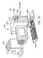
- Fig. 1 is a diagram for describing a configuration in which a developing unit 54 (51, 52, 53) and a photoconductor unit 75 are attached to and detached from a printer unit 10a.
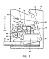
- Fig. 2 is a diagram showing main structural components that configure the printer 10. It should be noted that Fig. 2 is a diagram of a cross section taken perpendicular to the X direction in Fig. 1. Further, the up/down direction is shown by an arrow in Fig. 1 and Fig. 2, and for example, a paper supply tray 92 is arranged at a lower section of the printer 10 and a fusing unit 90 is arranged at an upper section of the printer 10.
- the developing unit 54 (51, 52, 53) and the photoconductor unit 75 can be attached to and detached from the printer unit 10a.
- the printer 10 is structured by attaching the developing unit 54 (51, 52, 53) and the photoconductor unit 75 to the printer unit 10a.
- the printer unit 10a has a first open/close cover 10b that can be opened and closed, a second open/close cover 10c that can be opened and closed and that is provided more to the inside than the first open/close cover 10b, a photoconductor unit attach/detach opening 10d through which the photoconductor unit 75 is attached and detached, and a developing unit attach/detach opening 10e through which the developing unit 54 (51, 52, 53) is attached and detached.
- the photoconductor unit 75 can be attached to and detached from the printer unit 10a via the photoconductor unit attach/detach opening 10d.
- the developing unit 54 (51, 52, 53) can be attached to and detached from the printer unit 10a via the developing unit attach/detach opening 10e.
- the printer 10 has a charging unit 30, an exposing unit 40, a YMCK developing device 50, a first transferring unit 60, an intermediate transferring body 70, and a cleaning blade 76, in the direction of rotation of a photoconductor 20, which is a latent image bearing body for bearing a latent image. It further includes a second transferring unit 80, a fusing unit 90, a display unit 95 made of a liquid crystal panel etc. for constituting a means for making a notification to the user, and a control unit 100 (Fig. 3) for controlling these units etc. so as to control the operation of the printer 10.
- the photoconductor 20 has a cylindrical conductive base and a photoconductive layer formed on the outer circumference surface of this base, and can rotate about a central shaft. In this embodiment, the photoconductor rotates in the clockwise direction as shown by an arrow in Fig. 2.
- the charging unit 30 is a device for charging the photoconductor 20
- the exposing unit 40 is a device for forming a latent image on the charged photoconductor 20 by irradiating laser.
- the exposing unit 40 has, for example, a semiconductor laser, a polygon mirror, and an F- ⁇ lens, and irradiates modulated laser onto the charged photoc onductor 20 based on an image signal that is input from a not-shown host computer, such as a personal computer or a word processor.
- the YMCK developing device 50 has a rotary 55, which serves as a moving body, and four developing units attached to the rotary 55.
- the rotary 55 is capable of rotating, and is provided with four attach/detach sections 55b, 55c, 55d, and 55e to and from which the four developing units 51, 52, 53, and 54 can respectively be attached and detached via the developing unit attach/detach opening 10d.
- the cyan developing unit 51 which contains cyan (C) toner, can be attached to and detached from the attach/detach section 55b
- the magenta developing unit 52 which contains magenta (M) toner
- the black developing unit 53 which contains black (K) toner
- the yellow developing unit 54 which contains yellow (Y) toner, can be attached to and detached from the attach/detach section 55e.
- the rotary 55 moves the above-mentioned four developing units 51, 52, 53, and 54 that have been attached to the attach/detach sections 55b, 55c, 55d, and 55e, respectively. That is, the rotary 55 rotates the four attached developing units 51, 52, 53, and 54 about a central shaft 55a while maintaining their relative positions. Then, the developing units 51, 52, 53, and 54 are selectively brought into opposition with the latent image formed on the photoconductor 20 so as to develop the latent image on the photoconductor 20 using the toner contained in each of the developing units 51, 52, 53, and 54. It should be noted that the developing units are described in detail later.
- the first transferring unit 60 is a device for transferring a single-color toner image formed on the photoconductor 20 onto the intermediate transferring body 70. When the four colors of toner are successively transferred over one another, a full-color toner image is formed on the intermediate transferring body 70.
- the intermediate transferring body 70 is an endless belt and is rotatively driven at substantially the same circumferential velocity as the photoconductor 20.
- a read sensor for synchronization RS is provided near the intermediate transferring body 70.
- the read sensor for synchronization RS is a sensor for detecting the reference position of the intermediate transferring body 70, and obtains a synchronization signal Vsync in the sub-scanning direction, which is perpendicular to the main scanning direction.
- the read sensor for synchronization RS has a light-emitting section for emitting light and a light-receiving section for receiving light.
- the read sensor for synchronization RS generates a pulse signal.
- One pulse signal is generated each time the intermediate transferring body 70 makes one revolution.
- the second transferring unit 80 is a device for transferring the single-color toner image or the full-color toner image formed on the intermediate transferring body 70 onto a recording medium such as paper, film, or cloth.
- the fusing unit 90 is a device for fusing the single-color toner image or the full-color toner image, which has been transferred onto the recording medium, onto the recording medium, such as paper, to make the image into a permanent image.
- the cleaning blade 76 is made of rubber and abuts against the surface of the photoconductor 20.
- the cleaning blade 76 removes the toner remaining on the photoconductor 20 by scraping it off after the toner image has been transferred onto the intermediate transferring body 70 by the first transferring unit 60.
- the photoconductor unit 75 is provided between the first transferring unit 60 and the exposing unit 40, and has the photoconductor 20, an element 75a to which information can be written, the charging unit 30, the cleaning blade 76, and a waste toner containing section 76a for containing toner that has been scraped off by the cleaning blade 76. It should be noted that the element 75a has a configuration that allows storage of various types of information that have been written in.
- the control unit 100 is made of a main controller 101 and a unit controller 102, as shown in Fig. 3.
- An image signal is input to the main controller 101, and in accordance with a command based on this image signal, the unit controller 102 controls each of the above-mentioned units etc. to form an image.
- the photoconductor 20 and the intermediate transferring body 70 are rotated due to control by the unit controller 102 based on a command from the main controller 101. Then, the reference position of the intermediate transferring body 70 is detected by the read sensor for synchronization RS, and a pulse signal is output. This pulse signal is sent to the unit controller 102 via a serial interface 121.
- the unit controller 102 controls the following operation, taking the pulse signal, which has been received, as a reference.
- the photoconductor 20 While rotating, the photoconductor 20 is successively charged by the charging unit 30 at a charging position.
- the area of the photoconductor 20 that has been charged is brought to an exposing position through the rotation of the photoconductor 20, and a latent image corresponding to image information for a first color, for example, yellow Y, is formed in that area by the exposing unit 40.
- the latent image formed on the photoconductor 20 is brought to a developing position through the rotation of the photoconductor 20, and is developed with yellow toner by the yellow developing unit 54. A yellow toner image is thus formed on the photoconductor 20.
- the yellow toner image that has been formed on the photoconductor 20 is brought to a first transferring position through the rotation of the photoconductor 20 and is transferred onto the intermediate transferring body 70 by the first transferring unit 60.
- a first transferring voltage that has a polarity that is opposite from the toner-charge polarity is applied to the first transferring unit 60.
- the second transferring unit 80 is separated from the intermediate transferring body 70.
- the full-color toner image that has been formed on the intermediate transferring body 70 is brought to a second transferring position through the rotation of the intermediate transferring body 70 and is transferred onto a recording medium by the second transferring unit 80.
- the recording medium is carried from the paper supply tray 92 to the second transferring unit 80 via a paper supply roller 94 and a resist roller 96.
- the second transferring unit 80 is pressed against the intermediate transferring body 70 and supplied with a second transferring voltage.
- the fusing unit 90 heats and applies pressure to the full-color toner image that has been transferred to the recording medium, and the image is fused to the recording medium.
- the toner adhering to its surface is scraped off by the cleaning blade 76 and it is prepared for charging for forming the next latent image.
- the toner that has been scraped off is collected in the waste toner containing section 76a.
- Fig. 3 is a block diagram showing the control unit 100 provided in the printer 10.
- the main controller 101 of the control unit 100 is connected to a host computer via the interface 112, and is provided with an image memory 113 for storing image signals that are received from the host computer.
- the unit controller 102 of the control unit 100 is electrically connected to each of the units (the charging unit 30, the exposing unit 40, the first transferring unit 60, the photoconductor unit 75, the second transferring unit 80, the fusing unit 90, and the display unit 95) and the YMCK developing device 50, and by receiving signals from the sensors provided in these components, the unit controller controls each of these units and the YMCK developing device 50 based on signals input from the main controller 101 as it detects the state of each of these units and the YMCK developing device 50.
- the structural components for driving each of these units and the YMCK developing device 50 Fig.
- FIG. 3 shows a photoconductor unit drive control circuit, a charging unit drive control circuit, an exposing unit drive control circuit 127, a YMCK developing device drive control circuit 125, a first transferring unit drive control circuit, a second transferring unit drive control circuit, a fusing unit drive control circuit, and a display unit drive control circuit.
- the exposing unit drive control circuit 127 connected to the exposing unit 40 has a pixel counter 127a that serves as consumption amount detection means for detecting the amount of consumption of developer.
- the pixel counter 127a counts the number of pixels that are input to the exposing unit 40. It should be noted that it is also possible to provide the pixel counter 127a in the exposing unit 40 or in the main controller 101. It should be noted that the number of pixels is the number of pixels in units of basic resolution of the printer 10, or in other words, the number of pixels of the image that is actually printed.
- the amount of consumption of toner T (the usage amount) is proportional to the number of pixels, and therefore, by counting the number of pixels, it is possible to detect the amount of consumption of toner T.
- an AC voltage is supplied from an AC voltage supply section 126a and a DC voltage is supplied from a DC voltage supply section 126b.
- the YMCK developing device drive control circuit 125 applies a voltage, which is obtained by superimpos ing the AC voltage and the DC voltage, to a developing roller at a suitable timing to form an alternating electric field between the developing roller and the photoconductor.
- the CPU 120 provided in the unit controller 102 is connected to a nonvolatile storage element (hereinafter, also referred to as "printer-side memory” ) 122 such as a serial EEPROM via the serial interface (I/F) 121.
- a nonvolatile storage element hereinafter, also referred to as "printer-side memory”
- serial interface I/F
- the CPU 120 is capable of wirelessly communicating with elements 51a, 52a, 53a, and 54a, which are respectively provided in/on the developing units 51, 52, 53, and 54, via the serial interface 121, a send/receive circuit 123, and a printer-side antenna (antenna for communicating with the developing unit elements) 124b.
- the CPU 120 is also capable of wirelessly communicating with the element 75a of the photoconductor unit 75 via the serial interface 121, the send/receive circuit 123, and a printer-side antenna (antenna for communicating with the photoconductor unit element) 124a.
- the antenna 124b for communicating with the developing unit elements, which serves as a writing member writes information into the elements 51a, 52a, 53a, and 54a of the developing units 51, 52, 53, and 54, respectively.
- the antenna 124b for communicating with the developing unit elements, which serves as a writing member is also capable of reading information from the elements 51a, 52a, 53a, and 54a of the developing units 51, 52, 53, and 54, respectively.
- the antenna 124a for communicating with the photoconductor unit element, which serves as a writing member writes information into the element 75a of the photoconductor unit 75.
- the antenna 124a for communicating with the photoconductor unit element, which serves as a write means can also read information from the element 75a of the photoconductor unit 75.
- FIG. 4 is a perspective view of the yellow developing unit 54 seen from the side of a developing roller 510.
- Fig. 5 is a cross-sectional view showing main structural components of the yellow developing unit 54. It should be noted that in Fig. 5 as well, the up/down direction is shown by an arrow, and for example, the central axis of the developing roller 510 is located lower than the central axis of the photoconductor 20. Further, in Fig. 5, the yellow developing unit 54 is shown in a state in which it is pos itioned at a developing position that is in opposition to the photoconductor 20.
- the YMCK developing device 50 is provided with the cyan developing unit 51, which contains cyan (C) toner, the magenta developing unit 52, which contains magenta (M) toner, the black developing unit 53, which contains black (K) toner, and the yellow developing unit 54, which contains yellow (Y) toner. Since the configuration of each of these developing units is the same, the yellow developing unit 54 is described below.
- the yellow developing unit 54 is provided with, for example, a developer containing section, that is, a first containing section 530 and a second containing section 535 for containing yellow toner T which serves as the developer, the element 54a, a housing 540, the developing roller 510 which serves as the developer bearing roller, a toner supply roller 550 for supplying toner T to the developing roller 510, and a restriction blade 560 for restricting the thickness of the layer of toner T that is bore on the developing roller 510.
- a developer containing section that is, a first containing section 530 and a second containing section 535 for containing yellow toner T which serves as the developer
- the element 54a a housing 540
- the developing roller 510 which serves as the developer bearing roller
- a toner supply roller 550 for supplying toner T to the developing roller 510
- a restriction blade 560 for restricting the thickness of the layer of toner T that is bore on the developing roller 510.
- the housing 540 is manufactured by joining, for example, an upper housing and a lower housing which have been integrally molded, and the inside of the housing is divided into the first containing section 530 and the second containing section 535 by a restriction wall 545 that extends upward from the lower section (in the up/down direction of Fig. 5 ).
- the first containing section 530 and the second containing section 535 form developer containing sections (530, 535) for containing toner T which serves as a developer.
- the upper sections of the first containing section 530 and the second containing section 535 are in communication, and the movement of the toner T between them is restricted by the restriction wall 545.
- each of the developing units (the cyan developing unit 51, the magenta developing unit 52, the black developing unit 53, and the yellow developing unit 54) rotates in conjunction with the rotation of the rotary 55 so that the toner T in each developing unit is stirred. Therefore, a stirring member is not provided in the first containing section 530 or the second containing section 535.
- the element 54a into which information can be written, is provided on the outer surface of the housing 540.
- the element 54a has a configuration that allows written information to be stored.
- the longitudinal direction of the element 54a intersects with the longitudinal direction of the yellow developing unit 54. More preferably, it is also possible to achieve a configuration in which the longitudinal direction of the element 54a is perpendicular to the longitudinal direction of the yellow developing unit 54.
- the element 54a will be described in greater detail later, but here it should be noted that the element 54a is provided with an antenna 54d, and that the longitudinal direction of the antenna 54a also intersects with the longitudinal direction of the yellow developing unit 54.
- An opening 541 that communicates with the outside of the housing 540 is provided in the lower section of the first containing section 530.
- the toner supply roller 550 is provided in the first containing section 530 with its circumferential surface facing the opening 541, and is rotatably supported on the housing 540. Further, the developing roller 510 is provided with its circumferential surface facing the opening 541 from outside the housing 540, and the developing roller 510 abuts against the toner supply roller 550.
- the developing roller 510 bears toner T and carries the toner to a developing position, which is in opposition to the photoconductor 20.
- the developing roller 510 is made of, for example, aluminum, stainless steel, or iron, and if necessary, it can be subjected to nickel plating or chromium plating, and the toner bearing region can be subjected to sandblasting or the like. Further, the developing roller 510 can rotate about its central axis, and as shown in Fig. 5, it rotates in the opposite direction (in Fig. 5, the counterclockwise direction) to the rotating direction of the photoconductor 20 (in Fig. 5, the clockwise direction). Its central axis is located lower than the central axis of the photoconductor 20.
- the toner supply roller 550 supplies, to the developing roller 510, the toner T contained in the first containing section 530 and the second containing section 535.
- the toner supply roller 550 is made of polyurethane foam, for example, and abuts against the developing roller 510 in a state in which it is elastically deformed.
- the toner supply roller 550 is arranged at a lower section of the first containing section 530, and the toner T contained in the first containing section 530 and the second containing section is supplied to the developing roller 510 by the toner supply roller 550 at the lower section of the first containing section 530.
- the toner supply roller 550 can rotate about its central axis, and its central axis is located lower than the central rotation axis of the developing roller 510. Further, the toner supply roller 550 rotates in the opposite direction (in Fig. 5, the clockwise direction) to the rotating direction of the developing roller 510 (in Fig. 5, the counterclockwise direction). It should be noted that the toner supply roller 550 has the function of supplying the toner T that is contained in the first containing section 530 and the second containing section 535 to the developing roller 510 as well as the function of stripping off, from the developing roller 510, the toner T that remains on the developing roller 510 after development.
- the restriction blade 560 restricts the thickness of the toner T layer borne by the developing roller 510, and gives charge to the toner T borne by the developing roller 510.
- the restriction blade 560 has a rubber section 560a and a rubber support section 560b.
- the rubber section 560a is made of, for example, silicone rubber or urethane rubber
- the rubber support section 560b is a thin plate made of, for example, phosphor bronze or stainless steel, and has a springy characteristic.
- the rubber section 560a is supported by the rubber support section 560b, and one end of the rubber support section 560b is fixed to a blade support metal plate 562.
- the blade support metal plate 562 is fastened to a seal frame 526, which is described later, and is attached to the housing 540 together with the restriction blade 560, forming a part of a seal unit 520, which is described later.
- the rubber section 560a is pressed against the developing roller 510 by the elastic force created by the flexure of the rubber support section 560b.
- a blade backing member 570 made of Moltoprene or the like is provided on one side of the restriction blade 560 opposite from the side of developing roller 510.
- the blade backing member 570 prevents the toner T from entering in between the rubber support section 560b and the housing 540 to stabilize the elastic force caused by the flexure of the rubber support section 560b, and also presses the rubber section 560a against the developing roller 510 by applying force to the rubber section 560a toward the developing roller 510 from directly behind the rubber section 560a. Consequently, the blade backing member 570 improves the contact uniformity and the sealing properties of the rubber section 560a with respect to the developing roller 510.
- the end of the restriction blade 560 on the side opposite from the side supported by the blade support metal plate 562, that is, its tip, is not in contact with the developing roller 510; rather, a section at a predetermined distance from its tip contacts, with some breadth, the developing roller 510. That is, the restriction blade 560 does not abut against the developing roller 510 at its edge but rather at its mid section. Further, the restriction blade 560 is arranged such that its tip is facing upstream in the rotating direction of the developing roller 510, and thus, makes a so-called counter-abutment with respect to the roller. It should be noted that the abutting position where the restriction blade 560 abuts against the developing roller 510 is located lower than the central axis of the developing roller 510 and is also located lower than the central axis of the toner supply roller 550.
- the seal member 520 prevents the toner T in the yellow developing unit 54 from spilling out from the unit, and also collects the toner T on the developing roller 510, which has passed the developing position, into the developing unit without scraping it off.
- the seal member 520 is a seal made of polyethylene film or the like.
- the seal member 520 is supported by a seal support metal plate 522, and is attached to the frame 540 via the seal support metal plate 522.
- a seal urging member 524 made of Moltoprene or the like is provided on one side of the seal member 520 opposite from the side of the developing roller 510, and due to the elastic force of the seal urging member 524, the seal member 520 is pressed against the developing roller 510. It should be noted that the abutting position where the seal member 520 abuts against the developing roller 510 is located above the central axis of the developing roller 510.
- the toner supply roller 550 supplies , to the developing roller 510, the toner T that is contained in the first containing section 530 and the second containing section 535, which serve as developer containing sections.
- the toner T that is supplied to the developing roller 510 is brought to the abutting position of the restriction blade 560 in conjunction with the rotation of the developing roller 510, and when it passes the abutting position, the thickness of the toner layer is restricted and the toner is charged.
- the toner T on the developing roller 510 is brought to the developing position opposing the photoconductor 20, and is used for developing the latent image formed on the photoconductor 20 under the alternating electric field at the developing position.
- the toner T on the developing roller 510 that has passed the developing position due to further rotation of the developing roller 510 passes the seal member 520 and is collected into the developing unit by the seal member 520 without being scraped off.
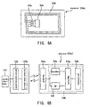
- Fig. 6A is a plan perspective view showing the configuration of an element.
- Fig. 6B is a block diagram for describing the internal configuration of the element and the send/receive section.
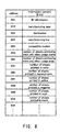
- Fig. 7 is a diagram for describing the information stored in a memory cell 54h of the element 54a.
- Fig. 8 is a diagram for describing the information stored in the memory cell of the element 54a of the photoconductor unit 75.
- the element 54a of the yellow developing unit 54 is taken as an example and described below.
- the element 54a and the printer-side antenna 124b are in a predetermined positional relationship, for example, if they are within 10 mm of one another, information can be sent and received without the element and the antenna being in contact with one another.
- the element 54a is overall very compact and thin, and one of its sides can be made adhesive and can be made to adhere to an object as a sticker. It is known as a memory tag, for example, and is sold commercially in various forms.
- the element 54a has a non-contact IC chip 54b, a resonant capacitor 54c that is formed by etching a metal film, and a flat coil serving as an antenna 54d. These are mounted onto a plastic film and covered by a transparent coversheet.
- the printer unit 10a has a coil that serves as the printer-side antenna 124b, the send/receive circuit 123, and the serial interface 121 that is connected to the controller (CPU) 120 of the printer unit 10a.
- the non-contact IC chip 54b has a rectifier 54e, a signal analysis section RF (Radio Frequency) 54f, a controller 54g, and the memory cell 54h.
- the memory cell 54h is a nonvolatile memory that can be electrically read and written, such as an NAND flash ROM, and is capable of storing information that has been written and allows the stored information to be read from the outside.
- the antenna 54d of the element 54a and the printer-side antenna 124b wirelessly communicate with one another to read information stored in the memory cell 54h andwrite information into the memory cell 54h. Further, the high frequency signals that are generated by the send/receive circuit 123 of the printer unit 10a are induced as a high frequency magnetic field via the printer-side antenna 124b. This high frequency magnetic field is absorbed via the antenna 54d of the element 54a, is rectified by the rectifier 54e, and becomes a DC power source for driving each of the circuits in the IC chip 54b.
- the memory cell 54h of the element 54a stores various types of information, as shown in Fig. 7.
- the address 00H stores unique ID information for each element, such as the serial number of the element.
- the address 01H stores the date that the developing unit was manufactured.
- the address 02H stores information for specifying the destination of the developing unit.
- the address 03H stores information for specifying the manufacturing line on which the developing unit was manufactured.
- the address 04H stores information for specifying models with which the developing unit is compatible.
- the address 05H stores toner remaining amount information as information indicating the amount of toner that is contained in the developing unit.
- the address 06H and subsequent areas store appropriate information.
- the ID information that is stored on the memory cell 54h of the element 54a can be written at the time that the storage element is manufactured in the factory.
- the main unit of the printer 10 can read this ID information to identify each of the elements 54a, 51a, 52a, and 53a.
- the element 75a of the photoconductor unit 75 has the same configuration.
- the memory cell of the element of the photoconductor unit 75 stores various types of information, as shown in Fig. 8.
- the address 00H stores unique ID information for each element, such as the serial number of the element.
- the address 01H stores the date that the photoconductor unit was manufactured.
- the address 02H stores information for specifying the destination of the photoconductor unit.
- the address 03H stores information for specifying the manufacturing line on which the photoconductor unit was manufactured.
- the address 04H stores information for specifying models with which the photoconductor unit is compatible.
- the address 05H stores information indicating the total number of printed sheets of the printer unit 10a when the photoconductor unit is attached to the printer unit 10a.
- the address 06H stores information indicating the total number of printed sheets of the printer unit 10a when the photoconductor unit has reached its service life and is detached from the printer unit 10a.
- the address 07H stores the number of sheets for which color printing has been performed using the photoconductor unit.
- the address 08H stores the number of sheets for which monochrome printing has been performed using the photoconductor unit.
- the address 09H stores the number of sheets developed by the yellow developing unit 54, that is, the number of sheets printed using yellow toner.
- the address OAH stores the number of sheets developed by the magenta developing unit 52, that is, the number of sheets printed using magenta toner.
- the address 0BH stores the number of sheets developed by the cyan developing unit 51, that is, the number of sheets printed using cyan toner.
- the address 0CH stores the number of sheets developed by the black developing unit 53, that is, the number of sheets printed using black toner.
- the address ODH and subsequent areas store appropriate information.
- Fig. 9A is a diagram for describing the relationship between the element and the printer-side antenna when the yellow developing unit 54 is positioned at the developing position.
- Fig. 9B is a diagram for describing the relationship between the element and the printer-side antenna when the yellow developing unit 54 is positioned at the attach/detach position.
- Fig. 9C is a diagram for describing the relationship between the element and the printer-side antenna when the rotary 55 is positioned at the home position.
- the yellow developing unit 54 is positioned at the developing position (opposing position), and the element 54a of the yellow developing unit 54 is in opposition to the printer-side antenna 124b in a non-contact state.
- the printer-side antenna 124b is provided so that its longitudinal direction (in Fig. 9A, the Y direction) is in the direction of rotation of the rotary 55 (in Fig. 9A, the Z direction).
- the printer-side antenna 124b can wirelessly communicate with the element 54a not only in the state shown in Fig. 9A but also in a state in which the rotary 55 has been rotated by a predetermined angle.
- the longitudinal direction of the printer-side antenna 124b follow the direction of rotation of the rotary 55, the range of angle of rotation of the rotary 55 in which wireless communication is possible can be made large.
- the length of the printer-side antenna 124b in the longitudinal direction is longer than the length of the element 54a in that longitudinal direction.
- the printer-side antenna 124b is provided more to the outside than the element 54a in the radial direction of rotation of the rotary 55.
- the printer-side antenna 124b which is provided more to the outside than the element 54a in the radial direction of rotation of the rotary 55, effective wireless communication with respect to the element 54a of the yellow developing unit 54 can be achieved.
- the printer-side antenna 124b can wirelessly communicate with the element 54a not only when the rotary 55 is in a stopped state but also when the rotary 55 is in a moving state. That is, the printer-side antenna 124b can wirelessly communicate with the element 54a even if the element is moving.
- printer-side antenna 124a is in opposition to the element 75a of the photoconductor unit 75 in a non-contact state (see Fig. 2), and the printer-side antenna 124a can wirelessly communicate with the element 75a of the photoconductor unit 75 in a non-contact state.
- the yellow developing unit 54 is positioned at the developing position.
- the state shown in Fig. 9B is attained.
- the yellow developing unit 54 is positioned at the developing position.
- the yellow developing unit 54 can be attached and detached via the attach/detach opening 10e, that is, it can be mounted to the attach/detach section 55e or it can be removed from the attach/detach section 55e.
- the cyan developing unit 51 which is positioned upstream in the direction of rotation of the rotary 55, is positioned at the developing position.
- Fig. 9C shows a state in which the rotary 55 is positioned at the home position after the printer 10 has been turned ON and the initialization operation has been performed.
- Fig. 10 is a flowchart for describing how information is written into the elements of the developing units.
- Step 1 Step of Standby for Image Forming Process
- the printer 10 When the printer 10 is turned ON, a predetermined initialization operation is performed, and the printer 10 enters an image forming process standby state.
- an image signal which is an image forming process command from the host computer, is input to the main controller 101 of the printer 10 via the interface (I/F) 112, the photoconductor 20 and the intermediate transferring body 70 are rotated. Then, the read sensor for synchronization RS detects the reference position of the intermediate transferring body 70 and outputs a pulse signal.
- the unit controller 102 executes the following control, taking the pulse signal that has been received as a reference.
- Step 3 Step of Starting Counting Number of Yellow Pixels
- a latent image that corresponds to the yellow image information is formed on the charged photoconductor by the exposing unit 40.
- the pixel counter 127a starts counting the number of pixels that are input to the exposing unit 40.
- Step 5 Step of Moving Yellow Developing Unit
- the rotary 55 is rotated, and the yellow developing unit 54 is moved to the developing position.
- Step 7 Step of Starting Application of Yellow Developing Bias
- the developing bias that is applied is a voltage obtained by superimposing an AC voltage and a DC voltage, as mentioned above. It should be noted that the developing bias may be applied to the developing roller before the yellow developing unit 54 arrives at the developing position, or the developing bias may be applied to the developing roller after the yellow developing unit 54 arrives at the developing position.
- Step 9 Step of Ending Application of Yellow Developing Bias
- Step 11 Step of Obtaining Number of Yellow Pixels
- the number of pixels that have been counted is obtained from the pixel counter 127a.
- the number of counted pixels is proportional to the amount of consumption of toner, and thus the amount of consumption of yellow toner YT can be found.
- Step 13 Step of Reading and Storing Yellow Toner Remaining Amount
- the remaining amount of yellow toner YY that is stored in the RAM is read out from the RAM, and a value YYnew obtained by subtracting the consumption amount YT from the remaining amount YY is stored in the RAM as the new remaining amount.
- Step 15 Step of Starting Movement of Cyan Developing Unit
- the rotary 55 starts rotating so as to position the cyan developing unit 51 at the developing position.
- the value YYnew obtained by subtracting the consumption amount YT from the remaining amount YY is written into the element 54a of the yellow developing unit 54.
- This writing is carried out using the printer-side antenna 124b, without it being in contact with the element 54a which is moving. It should be noted that when this writing is carried out, the yellow developing unit 54 has not reached the detaching position (the attach/detach position) where it can be detached via the attach/detach opening 10e.
- Step 19 Step of Starting Counting Number of Cyan Pixels
- a latent image that corresponds to the cyan image information is formed on the charged photoconductor by the exposing unit 40.
- the pixel counter 127a starts counting the number of pixels that are input to the exposing unit 40.
- the rotation of the rotary 55 for positioning the cyan developing unit 51 at the developing position is ended.
- the cyan developing unit 51 arrives at the developing pos ition.
- the number of pixels that have been counted is obtained from the pixel counter 127a.
- the number of counted pixels is proportional to the amount of consumption of toner, and thus the amount of consumption of cyan toner CT can be found.
- the remaining amount of cyan toner CC that is stored in the RAM is read out from the RAM, and a value CCnew obtained by subtracting the consumption amount CT from the remaining amount CC is stored in the RAM as the new remaining amount.
- Step 29 Step of Starting Movement of Magenta Developing Unit
- the rotary 55 starts rotating so as to position the magenta developing unit 52 at the developing position.
- the value CCnew obtained by subtracting the consumption amount CT from the remaining amount CC is written into the element 51a of the cyan developing unit 51.
- This writing is carried out using the printer-side antenna 124b, without it being in contact with the element 51a which is moving. It should be noted that when this writing is carried out, the cyan developing unit 51 has not reached the detaching position (the attach/detach position) where it can be detached via the attach/detach opening 10e.
- Step 33 Step of Starting Counting Number of Magenta Pixels
- a latent image that corresponds to the magenta image information is formed on the charged photoconductor by the exposing unit 40.
- the pixel counter 127a starts counting the number of pixels that are input to the exposing unit 40.
- the rotation of the rotary 55 for positioning the magenta developing unit 52 at the developing position is ended.
- the magenta developing unit 52 arrives at the developing position.
- the number of pixels that have been counted is obtained from the pixel counter 127a.
- the number of counted pixels is proportional to the amount of consumption of toner, and thus the amount of consumption of magenta toner MT can be found.
- the remaining amount of magenta toner MM that is stored in the RAM is read out from the RAM, and a value MMnew obtained by subtracting the consumption amount MT from the remaining amount MM is stored in the RAM as the new remaining amount.
- Step 45 Step of Starting Movement of Black Developing Unit
- the rotary 55 starts rotating so as to position the black developing unit 53 at the developing position.
- the value MMnew obtained by subtracting the consumption amount MT from the remaining amount MM is written into the element 52a of the magenta developing unit 52.
- This writing is carried out using the printer-side antenna 124b, without it being in contact with the element 52a which is moving. It should be noted that when this writing is carried out, the magenta developing unit 52 has not reached the detaching position (the attach/detach position) where it can be detached via the attach/detach opening 10e.
- Step 49 Step of Starting Counting Number of Black Pixels
- a latent image that corresponds to the black image information is formed on the charged photoconductor by the exposing unit 40.
- the pixel counter 127a starts counting the number of pixels that are input to the exposing unit 40.
- the rotation of the rotary 55 for positioning the black developing unit 53 at the developing position is ended.
- the black developing unit 53 arrives at the developing position.
- Step 53 Step of Starting Application of Black Developing Bias
- Step 57 Step of Obtaining Number of Black Pixels
- the number of pixels that have been counted is obtained from the pixel counter 127a.
- the number of counted pixels is proportional to the amount of consumption of toner, and thus the amount of consumption of black toner BT can be found.
- Step 59 Step of Reading and Storing Black Toner Remaining Amount
- the remaining amount of black toner BB that is stored in the RAM is read out from the RAM, and a value BBnew obtained by subtracting the consumption amount BT from the remaining amount BB is stored in the RAM as the new remaining amount.
- Step 61 Step of Starting Movement to Home Position
- Rotation of the rotary 55 is started so as to position the rotary 55 at the home position.
- Step 63 Step of Writing Information into Element 53a (Step 63) >
- the value BBnew obtained by subtracting the consumption amount BT from the remaining amount BB is written into the element 53a of the black developing unit 53.
- This writing is carried out using the printer-side antenna 124b, without it being in contact with the element 53a which is moving. It should be noted that when this writing is carried out, the black developing unit 53 has not reached the detaching position (the attach/detach position) where it can be detached via the attach/detach opening 10e.
- Step 65 Step of Ending Printing Operation
- printer-side antenna 124b which serves as a writing member, can write information into the element of a developing unit during the period from when that developing unit arrives at the opposing position (developing position) until it arrives at the detaching position (attach/detach position) due to movement of the rotary 55.
- the writing member writes information into the element of a developing unit during the period from after developing of the latent image by the developer bearing body provided in that developing unit that has arrived at the opposing position has ended until when that developing unit arrives at the detaching position.
- the amount of developer in a developing unit decreases when the latent image is developed by the developer bearing body provided in that developing unit.
- information is written to the element of the developing unit by the writing member during the period from after developing of the latent image by the developer bearing body provided in that developing unit that has arrived at the opposing position has ended until when that developing unit arrives at the detaching position. Consequently, information about the remaining amount, for example, based on the amount of developer that has been reduced by development is written to the element of the developing unit.
- the writing member writes information to the element of a developing unit during a period from when the developing unit starts moving from the opposing position until when the developing unit arrives at the detaching position due to movement of the rotary 55.
- the time from when the developing unit starts moving from the opposing position until it arrives at the detaching position can be utilized to effectively write information.
- the yellow developing unit 54 arrived at the attach/detach position where it can be attached and detached, and then when the rotary 55 rotated further, the cyan deve loping unit 51 upstream in the direction of rotation arrived at the developing position.
- the yellow developing unit 54 arrives at the attach/detach position where it can be attached and detached.
- the printer-side antenna 124b writes information to the element of the developing unit during a period until the other developing unit arrives at the developing position.
- the printer-side antenna 124b writes information to the element of said developing unit during a period until the other developing unit arrives at the developing position, and thus even if, for example, the developing unit is forcibly detached after the other developing unit arrives at the developing position, information will have already been written to the element of said developing unit.
- the printer-side antenna 124b writes information to an element when the AC voltage supply section 126a is not supplying AC voltage to the developing roller 510.
- information can be written accurately without being affected by the noise caused by supplying AC voltage to the developing roller 510, for example.
- Fig. 11 is a flowchart showing an example in which information is written into the element 75a of the photoconductor unit 75. More specifically, an example is shown in which the number of sheets printed by each developing unit, that is, the number of sheets printed by each toner color, is written into the element 75a.
- Step 101 Step of Standby for Image Forming Process
- the printer 10 When the printer 10 is turned ON, a predetermined initialization operation is performed, and the printer 10 enters an image forming process standby state.
- an image signal which is an image forming process command from the host computer, is input to the main controller 101 of the printer 10 via the interface (I/F) 112, the photoconductor 20 and the intermediate transferring body 70 are rotated. Then, the read sensor for synchronization RS detects the reference position of the intermediate transferring body 70 and outputs a pulse signal.
- the unit controller 102 executes the following control, taking the pulse signal that has been received as a reference.
- Step 105) ⁇ Step of Moving Yellow Developing Unit (Step 105) >
- the rotary 55 moves so as to position the yellow developing unit 54 at the developing position.
- Step 107 Step of Starting Application of Yellow Developing Bias
- the developing bias that is applied is a voltage obtained by superimposing an AC voltage and a DC voltage, as mentioned above. It should be noted that the developing bias may be applied to the developing roller before the yellow developing unit 54 arrives at the developing position, or the developing bias may be applied to the developing roller after the yellow developing unit 54 arrives at the developing position.
- Step 109 Step of Ending Application of Yellow Developing Bias
- Step 115 Step of Starting Movement of Cyan Developing Unit
- the rotary 55 starts rotating so as to position the cyan developing unit 51 at the developing position.
- Step 117 Step of Writing Information into Element 75a
- the method for writing information indicating that the number of sheets printed by the yellow developing unit 54 has increased by one sheet it is possible to adopt, for example, a method of storing data indicating the total number of sheets printed by the yellow developing unit 54 in a RAM provided in the printer unit 10a and then writing, into the element 75a of the photoconductor unit 75, a value obtained by adding 1 to the above-mentioned data.
- the rotation of the rotary 55 for positioning the cyan developing unit 51 at the developing position is ended.
- the cyan developing unit 51 arrives at the developing position.
- Step 125 Step of Ending Application of Cyan Developing Bias
- Step 129) Step of Starting Movement of Magenta Developing Unit
- the rotary 55 starts rotating so as to position the magenta developing unit 52 at the developing position.
- the rotation of the rotary 55 for positioning the magenta developing unit 52 at the developing position is ended.
- the magenta developing unit 52 arrives at the developing position.
- Step 137 Step of Starting Application of Magenta Developing Bias
- Step 139 Step of Ending Application of Magenta Developing Bias
- Step 145) Step of Starting Movement of Black Developing Unit
- the rotary 55 starts rotating so as to position the black developing unit 53 at the developing position.
- the rotation of the rotary 55 for positioning the black developing unit 53 at the developing position is ended.
- the black developing unit 53 arrives at the developing position.
- Step 153 Step of Starting Application of Black Developing Bias
- Step 155) Step of Ending Application of Black Developing Bias
- Step 165 Step of Ending Printing Operation
- printer-side antenna 124a which serves as a writing member, can write information into the element 75a of the photoconductor unit 75 during the period from when a developing unit arrives at the opposing position (developing position) until it arrives at the detaching position (attach/detach position) due to movement of the rotary 55.
- the printer-side antenna 124a writes information to the element 75a of the photoconductor unit 75 during the period from after developing of the latent image by the developer bearing body provided in that developing unit that has arrived at the opposing position has ended until when that developing unit arrives at the detaching position.
- the amount of developer in a developing unit decreases when the latent image is developed by the developer bearing body provided in that developing unit.
- information is written to the element 75a of the photoconductor unit 75 by the printer-side antenna 124a during the period from after developing of the latent image by the developer bearing body provided in that developing unit that has arrived at the opposing position has ended until when that developing unit arrives at the detaching position. Consequently, information about the remaining amount, for example, based on the amount of developer that has been reduced by developing, and the number of sheets printed by each toner color, for example, can be written to the element 75a of the photoconductor unit 75.
- the printer-side antenna 124a writes information to the element 75a of the photoconductor unit 75 during a period from when the developing unit starts moving from the opposing position until when the developing unit arrives at the detaching position due to movement of the rotary 55.
- the time from when a developing unit starts moving from the opposing position until it arrives at the detaching position can be utilized to effectively write information.
- the yellow developing unit 54 arrived at the attach/detach position where it can be attached and detached, and then when the rotary 55 rotated further, the cyan developing unit 51 upstream in the direction of rotation arrived at the developing position.
- the yellow developing unit 54 has begun moving from the developing position, the cyan developing unit 51 upstream in the direction of rotation first arrives at the developing position, and then when the rotary 55 rotates further, the yellow developing unit 54 arrives at the attach/detach position where it can be attached and detached.
- the printer-side antenna 124a writes information to the element 75a of the photoconductor unit 75 during a period until the other developing unit arrives at the developing position.
- the printer-side antenna 124a writes information to the element 75a of the photoconductor unit 75 until the time that the other developing unit arrives at the developing position, and thus even if, for example, the developing unit is forcibly detached after the other developing unit arrives at the developing position, for example, information will have already been written to the element 75a.
- the printer-side antenna 124a writes information to the element 75a when the AC voltage supply section 126a is not supplying AC voltage to the developing roller 510.
- information can be written accurately without being affected by the noise caused by supplying AC voltage to the developing roller 510, for example.
- the information written into the element 75a is not limited to the foregoing example, and as shown in Fig. 8, it can also be, for example, the number of printed sheets when usage starts, the number of printed sheets when usage ends, or the number of sheets printed in monochrome.
- the antenna may assume any configuration. It should be noted that if the rotary 55 employed as the moving body moves rotatively, then the longitudinal direction of the printer-side antenna being in the direction of movement of the moving body means that the longitudinal direction of the printer-side antenna is in a tangential direction at a position in opposition to the printer-side antenna in the rotation radius of the rotary 55.
- Fig. 12 is a diagram showing a first alternative embodiment of the printer-side antenna. In Fig.
- a printer-side antenna 124c is provided at a position where it is in opposition to and extends over a first developing unit (the yellow developing unit 54) attached to a first attach/detach section and a second developing unit (the black developing unit 53) attached to a second attach/detach section that is adjacent to the first attach/detach section.
- a first developing unit the yellow developing unit 54
- a second developing unit the black developing unit 53
- the printer-side antenna 124c is in opposition to a first element of the first developing unit (the element 54a of the yellow developing unit 54), but it is also possible for the printer-side antenna 124c to be in opposition to a second element of the second developing unit (the element 53a of the black developing unit 53) as well.
- Fig. 13 is a diagram showing another embodiment regarding an arrangement for the elements.
- Fig. 14 is a diagram showing a second alternative embodiment of the printer-side antenna, and shows an arrangement seen from the inner side of the printer unit when the side of the printer unit 10a on which the first open/close cover 10b is provided is regarded as the front side.
- the element 54a is provided on a lateral surface of the yellow developing unit 54.
- This lateral surface is the lateral surface that becomes the front end side in the attaching direction when the yellow developing unit 54 is attached to the printer unit 10a via the attach/detach opening 10e.
- a printer-side antenna 124d is provided in opposition to the element 54a, as shown in Fig. 14. More specifically, the printer-side antenna 124d is provided more to the outside than the element 54a in the direction of the rotation axis of the rotary 55, that is, more towards the inward direction of the printer unit 10a than the element 54a, without being in contact with the element 54a.
- the printer-side antenna 124d which is provided more to the outside than the element 54a in the direction of the rotation axis of the rotary 55, can be used to effectively achieve wireless communication with respect to the elements of the developing units attached to the attach/detach sections provided in the rotary 55.
- the length of the printer-side antenna in the longitudinal direction is also possible for the length of the printer-side antenna in the longitudinal direction to be shorter than the length of the element in that longitudinal direction.
- a configuration in which the length of the printer-side antenna in the longitudinal direction is longer than the length of the element in that longitudinal direction is advantageous in terms that it allows wireless communication with respect to the elements of the developing units attached to the attach/detach sections provided in the moving body to be achieved more effectively.
- the moving body is not limited to a rotary-type member that moves rotatively, and it may also be a member that carries out translation operation.
- the printer-side antenna 124b can write information into the element of the developing unit attached to the attach/detach section when theAC voltage supply section 126a is not supplying an AC voltage to the charging unit 30.
- information can be written accurately without being affected by, for example, noise caused by supplying the AC voltage to the charging unit 30.
- the printer-side antenna 124b can write information into the element of the developing unit attached to the attach/detach section when the AC voltage supply section 126a is not supplying an AC voltage to the first transferring unit 60.
- information can be written accurately without being affected by, for example, noise caused by supplying the AC voltage to the first transferring unit 60.
- the present embodiment is particularly effective in image forming processing in which there is a large difference between the maximum voltage value and the minimum voltage value applied by the AC voltage supply section 126a.
- it is particularly effective in image forming apparatuses in which the difference between the maximum voltage value and the minimum voltage value is 1000 volts ormore.
- the difference between the maximum voltage value and the minimum voltage value of the AC voltage is 1000 volts or more, the electromagnetic noise that occurs also becomes large.
- the developing unit is not limited to a device of the configuration described in the foregoing embodiment, and it is applicable to any type of developing unit.
- the developing unit may be of any configuration as long as it has an element into which information can be written and a developer containing section.
- the developing unit does not have to include a developer bearing body, and the developing unit may be provided in the printer unit 10a.
- any material as the developer bearing roller such as magnetic material, non-magnetic material, conductive material, insulating material, metal, rubber, and resin, as long as it is possible to structure a developer bearing roller.
- the material it is possible to use: metal such as aluminum, nickel, stainless steel, and iron; rubber such as natural rubber, silicone rubber, urethane rubber, butadiene rubber, chloroprene rubber, neoprene rubber, and NBR; or resin such as styrene resin, vinyl chloride resin, polyurethane resin, polyethylene resin, methacrylate resin, and nylon resin. Further, it is without saying that these can be used even if the upper layer of these materials is coated.
- the coating material it is possible to use, for example, polyethylene, polystyrene, polyurethane, polyester, nylon, or acrylic resin. Further, it is possible to use any form, such as an inelastic body, an elastic body, a single-layer structure, a multi-layer structure, a film, and a roller. Further, the developer is not limited to toner, but it may be, for example, a two component developer in which a carrier is mixed.
- the toner supplying member as well, and as the material therefor, other than polyurethane foam described above, it is possible to use, for example, polystyrene foam, polyethylene foam, polyester foam, ethylene propylene foam, nylon foam, or silicone foam. It should be noted that, as the foam cells of the toner supplying means, both open-cell foams and closed-cell foams can be used. It should be noted that there is no limitation to foam material, and it is possible to use rubber material having elasticity.
- a material that is molded and in which a conductive agent such as carbon is dispersed into for example, silicone rubber, urethane rubber, natural rubber, isoprene rubber, styrene butadiene rubber, butadiene rubber, chloroprene rubber, butyl rubber, ethylene propylene rubber, epichlorohydrin rubber, nitrile butadiene rubber, or acrylic rubber.
- the photoconductor unit 75 also is not limited to the device of the configuration described in the foregoing embodiment, and it is applicable to any type of device. It is only necessary that the photoconductor unit 75 has an element into which information can be written and a photoconductor. For example, it does not have to include the charging unit 30, and instead, the charging unit may be provided in the printer unit 10a. Further, the photoconductor is not limited to a roller-shaped photoconductive roller, and it may also be belt-shaped.
- the elements of the developing units and the element of the photoconductor unit are not limited to the configuration described in the foregoing embodiment. It is only necessary that information can be written into them, and it is possible for them to be, for example, elements in which the antenna is provided separately.
- an intermediate transferring type full-color laser beam printer was described as an example of the image forming apparatus, but the present invention is also applicable to various other types of image forming apparatuses, such as full-color laser beam printers that are not of the intermediate transferring type, monochrome laser beam printers, copying machines, and facsimiles.
- Fig. 15 is an explanatory drawing showing an external structure of a computer system.
- the computer system 1000 comprises a computer unit 1102, a display device 1104 , a printer 1106, an input device 1108, and a reading device 1110.
- the computer unit 1102 is accommodated in a mini-tower type housing, but this is not a limitation.
- a CRT cathode ray tube
- a plasma display or a liquid crystal display device, for example
- the printer described above is used as the printer 1106.
- a keyboard 1108A and a mouse 1108B are used as the input device 1108, but this is not a limitation.
- a flexible disk drive device 1110A and a CD-ROM drive device 1110B are used as the reading device 1110, but the reading device is not limited to these, and it may also be other devices such as a MO (magneto optical) disk drive device and a DVD (digital versatile disk).
- MO magnetic optical
- DVD digital versatile disk
- Fig. 16 is a block diagram showing a configuration of the computer system shown in Fig. 15. Further provided are an internal memory 1202, such as a RAM inside the housing accommodating the computer unit 1102, and an external memory such as a hard disk drive unit 1204.
- an internal memory 1202 such as a RAM inside the housing accommodating the computer unit 1102
- an external memory such as a hard disk drive unit 1204.
- the computer system is structured by connecting the printer 1106 to the computer unit 1102, the display device 1104, the input device 1108, and the reading device 1110 was described, but this is not a limitation.
- the computer system can be made of the computer unit 1102 and the printer 1106, or the computer system does not have to comprise any one of the display device 1104, the input device 1108, and the reading device 1110.
- the printer 1106 can have some of the functions or mechanisms of the computer unit 1102, the display device 1104, the input device 1108, and the reading device 1110.
- the printer 1106 may be configured so as to have an image processing section for carrying out image processing, a displaying section for carrying out various types of displays, and a recording media attac h/detach section to and from which recording media storing image data captured by a digital camera or the like are inserted and taken out.
Landscapes
- Physics & Mathematics (AREA)
- General Physics & Mathematics (AREA)
- Engineering & Computer Science (AREA)
- Theoretical Computer Science (AREA)
- Human Computer Interaction (AREA)
- General Engineering & Computer Science (AREA)
- Dry Development In Electrophotography (AREA)
- Control Or Security For Electrophotography (AREA)
- Electrophotography Configuration And Component (AREA)
- Color Electrophotography (AREA)
Applications Claiming Priority (5)
| Application Number | Priority Date | Filing Date | Title |
|---|---|---|---|
| JP2002113947 | 2002-04-16 | ||
| JP2002113948 | 2002-04-16 | ||
| JP2002113948 | 2002-04-16 | ||
| JP2002113947 | 2002-04-16 | ||
| PCT/JP2003/004702 WO2003087953A1 (fr) | 2002-04-16 | 2003-04-14 | Dispositif de formation d'image, unite de mise au point et systeme informatique |
Publications (2)
| Publication Number | Publication Date |
|---|---|
| EP1498783A1 true EP1498783A1 (fr) | 2005-01-19 |
| EP1498783A4 EP1498783A4 (fr) | 2010-03-31 |
Family
ID=29253567
Family Applications (1)
| Application Number | Title | Priority Date | Filing Date |
|---|---|---|---|
| EP03746480A Withdrawn EP1498783A4 (fr) | 2002-04-16 | 2003-04-14 | Dispositif de formation d'image, unite de mise au point et systeme informatique |
Country Status (6)
| Country | Link |
|---|---|
| US (1) | US7340201B2 (fr) |
| EP (1) | EP1498783A4 (fr) |
| JP (2) | JP3994968B2 (fr) |
| KR (1) | KR100679768B1 (fr) |
| CN (1) | CN100383675C (fr) |
| WO (1) | WO2003087953A1 (fr) |
Cited By (1)
| Publication number | Priority date | Publication date | Assignee | Title |
|---|---|---|---|---|
| WO2005111734A1 (fr) | 2004-05-19 | 2005-11-24 | Canon Kabushiki Kaisha | Conteneur fournissant du toner et appareil de formation d'image, pour détecter la quantité de toner restante |
Families Citing this family (9)
| Publication number | Priority date | Publication date | Assignee | Title |
|---|---|---|---|---|
| WO2003087952A1 (fr) * | 2002-04-16 | 2003-10-23 | Seiko Epson Corporation | Dispositif de formation d'image, unite de mise au point et systeme informatique |
| US7224924B2 (en) * | 2004-02-13 | 2007-05-29 | Seiko Epson Corporation | Developing device, image forming apparatus, image forming system, and method of manufacturing developing device |
| WO2006062026A1 (fr) * | 2004-12-09 | 2006-06-15 | Seiko Epson Corporation | Appareil de developpement, appareil et systeme de formation d'image, cartouche, unite de developpement et unite de phororecepteur |
| JP5076470B2 (ja) * | 2006-12-05 | 2012-11-21 | 富士ゼロックス株式会社 | 画像形成装置、制御装置およびプログラム |
| JP2009042691A (ja) * | 2007-08-10 | 2009-02-26 | Ricoh Co Ltd | 画像形成装置及び管理システム |
| JP5365121B2 (ja) * | 2008-02-04 | 2013-12-11 | 株式会社リコー | トナー補給装置及び画像形成装置 |
| JP4948582B2 (ja) * | 2009-09-09 | 2012-06-06 | キヤノン株式会社 | 画像形成装置 |
| JP5855595B2 (ja) * | 2013-03-27 | 2016-02-09 | シャープ株式会社 | 画像形成装置 |
| JP7098929B2 (ja) * | 2017-12-27 | 2022-07-12 | ブラザー工業株式会社 | 画像形成装置 |
Citations (1)
| Publication number | Priority date | Publication date | Assignee | Title |
|---|---|---|---|---|
| EP0992862A2 (fr) * | 1998-10-09 | 2000-04-12 | Canon Kabushiki Kaisha | Appareil électrophotographique de formation d'images, unité de traitement, dispositif de développement, réservoir d'alimentation en développateur et élément de mesure associé |
Family Cites Families (19)
| Publication number | Priority date | Publication date | Assignee | Title |
|---|---|---|---|---|
| US5313233A (en) * | 1989-05-30 | 1994-05-17 | Canon Kabushiki Kaisha | Image forming apparatus |
| JPH09190139A (ja) | 1996-01-09 | 1997-07-22 | Canon Inc | プロセスカートリッジ、現像装置及び電子写真画像形成装置 |
| JPH10240084A (ja) | 1997-02-28 | 1998-09-11 | Canon Inc | 画像形成装置およびプロセスカートリッジ |
| JPH11338329A (ja) * | 1998-05-27 | 1999-12-10 | Canon Inc | 画像形成装置および装置ユニット |
| US6195519B1 (en) * | 1998-12-18 | 2001-02-27 | Ricoh Company, Ltd. | Image forming apparatus having power and control signal transfer to a revolver without contacting the revolver |
| JP3571584B2 (ja) | 1999-07-08 | 2004-09-29 | シャープ株式会社 | 画像形成装置 |
| JP2001125362A (ja) * | 1999-10-27 | 2001-05-11 | Canon Inc | プロセスカートリッジ、電子写真画像形成装置、画像形成装置、現像装置、現像剤容器及び測定部品 |
| JP2001147579A (ja) * | 1999-11-19 | 2001-05-29 | Canon Inc | 画像形成装置 |
| JP2001194887A (ja) * | 2000-01-07 | 2001-07-19 | Canon Inc | プロセスカートリッジおよび電子写真画像形成装置 |
| JP2001265103A (ja) * | 2000-01-13 | 2001-09-28 | Canon Inc | 画像形成装置 |
| JP2001209219A (ja) | 2000-01-26 | 2001-08-03 | Canon Inc | 画像形成装置およびその装置ユニット |
| JP2001228698A (ja) * | 2000-02-18 | 2001-08-24 | Canon Inc | 現像剤残量検出装置、現像装置、カートリッジ及び電子写真画像形成装置 |
| JP2001344575A (ja) | 2000-05-31 | 2001-12-14 | Denso Corp | 非接触式icカードシステム |
| JP4721203B2 (ja) | 2000-06-14 | 2011-07-13 | 大日本印刷株式会社 | 非接触式データキャリアおよびシリンダ装置 |
| JP2002014579A (ja) * | 2000-06-30 | 2002-01-18 | Canon Inc | 画像形成装置およびその装置ユニット |
| JP2002049206A (ja) | 2000-08-01 | 2002-02-15 | Canon Inc | 現像カートリッジ及び画像形成装置 |
| JP3893861B2 (ja) | 2000-08-18 | 2007-03-14 | 富士ゼロックス株式会社 | 画像形成装置及びこれに用いる交換部品 |
| JP3461330B2 (ja) | 2000-08-25 | 2003-10-27 | キヤノン株式会社 | 電子写真画像形成システム、電子写真画像形成装置、プロセスカートリッジ、及び、メモリー部材 |
| JP3882528B2 (ja) * | 2001-05-11 | 2007-02-21 | セイコーエプソン株式会社 | 画像形成装置 |
-
2003
- 2003-04-14 JP JP2003584834A patent/JP3994968B2/ja not_active Expired - Fee Related
- 2003-04-14 WO PCT/JP2003/004702 patent/WO2003087953A1/fr active Application Filing
- 2003-04-14 US US10/510,979 patent/US7340201B2/en not_active Expired - Fee Related
- 2003-04-14 CN CNB038085216A patent/CN100383675C/zh not_active Expired - Fee Related
- 2003-04-14 EP EP03746480A patent/EP1498783A4/fr not_active Withdrawn
- 2003-04-14 KR KR1020047016607A patent/KR100679768B1/ko not_active IP Right Cessation
-
2007
- 2007-04-23 JP JP2007113320A patent/JP3995024B2/ja not_active Expired - Fee Related
Patent Citations (1)
| Publication number | Priority date | Publication date | Assignee | Title |
|---|---|---|---|---|
| EP0992862A2 (fr) * | 1998-10-09 | 2000-04-12 | Canon Kabushiki Kaisha | Appareil électrophotographique de formation d'images, unité de traitement, dispositif de développement, réservoir d'alimentation en développateur et élément de mesure associé |
Non-Patent Citations (1)
| Title |
|---|
| See also references of WO03087953A1 * |
Cited By (3)
| Publication number | Priority date | Publication date | Assignee | Title |
|---|---|---|---|---|
| WO2005111734A1 (fr) | 2004-05-19 | 2005-11-24 | Canon Kabushiki Kaisha | Conteneur fournissant du toner et appareil de formation d'image, pour détecter la quantité de toner restante |
| US8280264B2 (en) | 2004-05-19 | 2012-10-02 | Canon Kabushiki Kaisha | Toner supply container and image forming apparatus, for detecting the amount of remaining toner |
| US8498546B2 (en) | 2004-05-19 | 2013-07-30 | Canon Kabushiki Kaisha | Toner supply container and image forming apparatus |
Also Published As
| Publication number | Publication date |
|---|---|
| JP2007193367A (ja) | 2007-08-02 |
| JPWO2003087953A1 (ja) | 2005-08-25 |
| KR20040106349A (ko) | 2004-12-17 |
| KR100679768B1 (ko) | 2007-02-06 |
| US7340201B2 (en) | 2008-03-04 |
| JP3995024B2 (ja) | 2007-10-24 |
| US20050232646A1 (en) | 2005-10-20 |
| CN100383675C (zh) | 2008-04-23 |
| WO2003087953A1 (fr) | 2003-10-23 |
| EP1498783A4 (fr) | 2010-03-31 |
| CN1646997A (zh) | 2005-07-27 |
| JP3994968B2 (ja) | 2007-10-24 |
Similar Documents
| Publication | Publication Date | Title |
|---|---|---|
| US7929884B2 (en) | Image forming apparatus, developing unit, and computer system | |
| KR100521287B1 (ko) | 화상 형성 장치 및 화상 형성 장치용 제어 방법 | |
| JP3995024B2 (ja) | 画像形成装置、及び、コンピュータシステム | |
| US7469117B2 (en) | Image forming apparatus, developing unit, and computer system | |
| US6889024B2 (en) | Image-forming apparatus and computer system | |
| KR100649804B1 (ko) | 화상 형성 장치 및 컴퓨터 시스템 | |
| JP4314036B2 (ja) | 画像形成装置及び画像形成装置の制御方法 | |
| JP4049205B2 (ja) | 画像形成装置 | |
| CN101071288A (zh) | 图像形成装置、显影单元和计算机系统 |
Legal Events
| Date | Code | Title | Description |
|---|---|---|---|
| PUAI | Public reference made under article 153(3) epc to a published international application that has entered the european phase |
Free format text: ORIGINAL CODE: 0009012 |
|
| 17P | Request for examination filed |
Effective date: 20041109 |
|
| AK | Designated contracting states |
Kind code of ref document: A1 Designated state(s): AT BE BG CH CY CZ DE DK EE ES FI FR GB GR HU IE IT LI LU MC NL PT RO SE SI SK TR |
|
| REG | Reference to a national code |
Ref country code: HK Ref legal event code: DE Ref document number: 1070434 Country of ref document: HK |
|
| A4 | Supplementary search report drawn up and despatched |
Effective date: 20100225 |
|
| 17Q | First examination report despatched |
Effective date: 20100607 |
|
| REG | Reference to a national code |
Ref country code: HK Ref legal event code: WD Ref document number: 1070434 Country of ref document: HK |
|
| STAA | Information on the status of an ep patent application or granted ep patent |
Free format text: STATUS: THE APPLICATION IS DEEMED TO BE WITHDRAWN |
|
| 18D | Application deemed to be withdrawn |
Effective date: 20131101 |