EP1488450B1 - Methods of treating a silicon carbide substrate for improved epitaxial deposition and resulting structures and devices - Google Patents
Methods of treating a silicon carbide substrate for improved epitaxial deposition and resulting structures and devices Download PDFInfo
- Publication number
- EP1488450B1 EP1488450B1 EP03737679.5A EP03737679A EP1488450B1 EP 1488450 B1 EP1488450 B1 EP 1488450B1 EP 03737679 A EP03737679 A EP 03737679A EP 1488450 B1 EP1488450 B1 EP 1488450B1
- Authority
- EP
- European Patent Office
- Prior art keywords
- silicon carbide
- wafer
- region
- dopant atoms
- carbide wafer
- Prior art date
- Legal status (The legal status is an assumption and is not a legal conclusion. Google has not performed a legal analysis and makes no representation as to the accuracy of the status listed.)
- Expired - Lifetime
Links
Images


Classifications
-
- C—CHEMISTRY; METALLURGY
- C30—CRYSTAL GROWTH
- C30B—SINGLE-CRYSTAL GROWTH; UNIDIRECTIONAL SOLIDIFICATION OF EUTECTIC MATERIAL OR UNIDIRECTIONAL DEMIXING OF EUTECTOID MATERIAL; REFINING BY ZONE-MELTING OF MATERIAL; PRODUCTION OF A HOMOGENEOUS POLYCRYSTALLINE MATERIAL WITH DEFINED STRUCTURE; SINGLE CRYSTALS OR HOMOGENEOUS POLYCRYSTALLINE MATERIAL WITH DEFINED STRUCTURE; AFTER-TREATMENT OF SINGLE CRYSTALS OR A HOMOGENEOUS POLYCRYSTALLINE MATERIAL WITH DEFINED STRUCTURE; APPARATUS THEREFOR
- C30B31/00—Diffusion or doping processes for single crystals or homogeneous polycrystalline material with defined structure; Apparatus therefor
-
- C—CHEMISTRY; METALLURGY
- C30—CRYSTAL GROWTH
- C30B—SINGLE-CRYSTAL GROWTH; UNIDIRECTIONAL SOLIDIFICATION OF EUTECTIC MATERIAL OR UNIDIRECTIONAL DEMIXING OF EUTECTOID MATERIAL; REFINING BY ZONE-MELTING OF MATERIAL; PRODUCTION OF A HOMOGENEOUS POLYCRYSTALLINE MATERIAL WITH DEFINED STRUCTURE; SINGLE CRYSTALS OR HOMOGENEOUS POLYCRYSTALLINE MATERIAL WITH DEFINED STRUCTURE; AFTER-TREATMENT OF SINGLE CRYSTALS OR A HOMOGENEOUS POLYCRYSTALLINE MATERIAL WITH DEFINED STRUCTURE; APPARATUS THEREFOR
- C30B29/00—Single crystals or homogeneous polycrystalline material with defined structure characterised by the material or by their shape
- C30B29/10—Inorganic compounds or compositions
- C30B29/36—Carbides
-
- C—CHEMISTRY; METALLURGY
- C30—CRYSTAL GROWTH
- C30B—SINGLE-CRYSTAL GROWTH; UNIDIRECTIONAL SOLIDIFICATION OF EUTECTIC MATERIAL OR UNIDIRECTIONAL DEMIXING OF EUTECTOID MATERIAL; REFINING BY ZONE-MELTING OF MATERIAL; PRODUCTION OF A HOMOGENEOUS POLYCRYSTALLINE MATERIAL WITH DEFINED STRUCTURE; SINGLE CRYSTALS OR HOMOGENEOUS POLYCRYSTALLINE MATERIAL WITH DEFINED STRUCTURE; AFTER-TREATMENT OF SINGLE CRYSTALS OR A HOMOGENEOUS POLYCRYSTALLINE MATERIAL WITH DEFINED STRUCTURE; APPARATUS THEREFOR
- C30B33/00—After-treatment of single crystals or homogeneous polycrystalline material with defined structure
-
- H—ELECTRICITY
- H01—ELECTRIC ELEMENTS
- H01L—SEMICONDUCTOR DEVICES NOT COVERED BY CLASS H10
- H01L21/00—Processes or apparatus adapted for the manufacture or treatment of semiconductor or solid state devices or of parts thereof
- H01L21/02—Manufacture or treatment of semiconductor devices or of parts thereof
- H01L21/04—Manufacture or treatment of semiconductor devices or of parts thereof the devices having potential barriers, e.g. a PN junction, depletion layer or carrier concentration layer
- H01L21/0445—Manufacture or treatment of semiconductor devices or of parts thereof the devices having potential barriers, e.g. a PN junction, depletion layer or carrier concentration layer the devices having semiconductor bodies comprising crystalline silicon carbide
- H01L21/0455—Making n or p doped regions or layers, e.g. using diffusion
- H01L21/046—Making n or p doped regions or layers, e.g. using diffusion using ion implantation
-
- H—ELECTRICITY
- H01—ELECTRIC ELEMENTS
- H01L—SEMICONDUCTOR DEVICES NOT COVERED BY CLASS H10
- H01L21/00—Processes or apparatus adapted for the manufacture or treatment of semiconductor or solid state devices or of parts thereof
- H01L21/02—Manufacture or treatment of semiconductor devices or of parts thereof
- H01L21/02104—Forming layers
- H01L21/02365—Forming inorganic semiconducting materials on a substrate
- H01L21/02367—Substrates
- H01L21/0237—Materials
- H01L21/02373—Group 14 semiconducting materials
- H01L21/02378—Silicon carbide
-
- H—ELECTRICITY
- H01—ELECTRIC ELEMENTS
- H01L—SEMICONDUCTOR DEVICES NOT COVERED BY CLASS H10
- H01L21/00—Processes or apparatus adapted for the manufacture or treatment of semiconductor or solid state devices or of parts thereof
- H01L21/02—Manufacture or treatment of semiconductor devices or of parts thereof
- H01L21/02104—Forming layers
- H01L21/02365—Forming inorganic semiconducting materials on a substrate
- H01L21/02436—Intermediate layers between substrates and deposited layers
- H01L21/02439—Materials
- H01L21/02491—Conductive materials
-
- H—ELECTRICITY
- H01—ELECTRIC ELEMENTS
- H01L—SEMICONDUCTOR DEVICES NOT COVERED BY CLASS H10
- H01L21/00—Processes or apparatus adapted for the manufacture or treatment of semiconductor or solid state devices or of parts thereof
- H01L21/02—Manufacture or treatment of semiconductor devices or of parts thereof
- H01L21/02104—Forming layers
- H01L21/02365—Forming inorganic semiconducting materials on a substrate
- H01L21/02656—Special treatments
- H01L21/02658—Pretreatments
-
- H—ELECTRICITY
- H10—SEMICONDUCTOR DEVICES; ELECTRIC SOLID-STATE DEVICES NOT OTHERWISE PROVIDED FOR
- H10H—INORGANIC LIGHT-EMITTING SEMICONDUCTOR DEVICES HAVING POTENTIAL BARRIERS
- H10H20/00—Individual inorganic light-emitting semiconductor devices having potential barriers, e.g. light-emitting diodes [LED]
- H10H20/01—Manufacture or treatment
- H10H20/011—Manufacture or treatment of bodies, e.g. forming semiconductor layers
- H10H20/013—Manufacture or treatment of bodies, e.g. forming semiconductor layers having light-emitting regions comprising only Group III-V materials
- H10H20/0133—Manufacture or treatment of bodies, e.g. forming semiconductor layers having light-emitting regions comprising only Group III-V materials with a substrate not being Group III-V materials
- H10H20/01335—Manufacture or treatment of bodies, e.g. forming semiconductor layers having light-emitting regions comprising only Group III-V materials with a substrate not being Group III-V materials the light-emitting regions comprising nitride materials
Definitions
- gallium nitride presents a particular set of technical problems in manufacturing working devices.
- the primary problem is the lack of bulk single crystals of gallium nitride which in turn means that gallium nitride or other group III-nitride devices must be formed as epitaxial layers on other materials.
- Sapphire i.e., aluminum oxide or Al 2 O 3
- Sapphire offers a reasonable crystal lattice match to Group III nitrides, thermal stability, and transparency, all of which are generally useful in producing a light emitting diode.
- Sapphire offers the disadvantage, however, of being an electrical insulator. This means that the electric current that is passed through an LED to generate the emission cannot be directed through the sapphire substrate.
- other types of connections to the LED must be made, such as placing both the cathode and anode of the device on the same side of the LED chip in a so-called "horizontal" configuration.
- an LED In general, it is preferable for an LED to be fabricated on a conductive substrate so that ohmic contacts can be placed at opposite ends of the device.
- Such devices called “vertical” devices, are preferred for a number of reasons, including their easier manufacture as compared to horizontal devices.
- silicon carbide can be conductively doped, and therefore can be effectively used to manufacture a vertical group III-nitride LED.
- silicon carbide has a relatively small lattice mismatch with gallium nitride, which means that high-quality group III-nitride material can be grown on it.
- Silicon carbide also has a high coefficient of thermal conductivity, which is important for heat dissipation in high-current devices such as laser diodes.
- silicon carbide-based group III-nitride LEDs are shown in U.S. Patents 5,523,589 ; 6,120,600 ; and 6,187,606 each of which is assigned to Cree, Inc., the assignee of the present invention.
- Such devices typically comprise a silicon carbide substrate, a buffer layer or region formed on the substrate, and a plurality of group III-nitride layers forming a p-n junction active region.
- U.S. Patent No. 6,187,606 represents an important advance over the state of the art as it previously existed.
- the invention described in the '606 patent provided a plurality of discrete crystal portions, or "dots", of GaN or InGaN on the substrate in an amount sufficient to minimize or eliminate the heterobarrier between the substrate and the buffer layer. A highly conductive path between the substrate and the active region could thereby be established.
- V f forward voltage
- V f forward voltage
- a silicon carbide substrate for improved epitaxial deposition thereon and for use as a precursor in the manufacture of devices such as light emitting diodes, the method comprising:
- the invention also provides a silicon carbide structure comprising:
- Devices include a light emitting device comprising a silicon carbide substrate having a predetermined conductivity type and first and second surfaces, a conductive buffer layer on the first surface of the substrate, and an active region on the conductive buffer, wherein the first surface of the substrate has a first implantation profile of implanted dopants of the predetermined conductivity type adjacent the first surface.
- device 10 comprises a conductive silicon carbide substrate 12 having a first conductivity type and having a first surface 12A and a second surface 12B.
- Device 10 further includes a conductive buffer region 14 formed on surface 12A of substrate 12 and an active region 18 formed on the conductive buffer 14.
- Active region 18 preferably includes a p-n junction and most preferably comprises a single heterostructure, double heterostructure, single quantum well, multiple quantum well or the like.
- a first ohmic contact 22 is formed on the surface of the active region.
- a second ohmic contact 24 is formed on the surface of the substrate.
- substrate 12 comprises n-type 4H-silicon carbide.
- ohmic contact 22 comprises the anode of the device 10 while ohmic contact 24 comprises the cathode of the device 10.
- Ohmic contact 24 may be formed according to the methods described in U.S. Patent Application Serial No. 09/787,189 filed March 15, 2001 published as US 688464 on 25 April 2005 .
- Substrate 12 includes a first implanted region 20 adjacent to surface 12A and comprising implanted dopant atoms of the first conductivity type. The presence of implanted region 20 causes a reduction in the voltage drop observable at the interface between substrate 12 and buffer region 14, which results in a reduction in the overall forward operating voltage (V f ) of the device 10.
- the implanted region has a peak concentration of implanted dopant atoms of between about 1E19 and 5E21 cm -3 and is between about 1 and 500 nm thick.
- the implanted region has a peak concentration of implanted dopant atoms of about 1E21 cm -3 and is about 50 nm thick.
- FIG. 2 illustrates a method of fabrication of doped structures.
- a silicon carbide substrate 12 is provided having a first conductivity type and having first surface 12A and second surface 12B.
- the fabrication of doped silicon carbide substrates such as substrate 12 is well known in the art.
- U.S. Patent RE34,861 discloses a process for growing boules of silicon carbide via controlled seeded sublimation.
- the resulting silicon carbide crystal may exhibit one of a number of polytypes, such as 4H, 6H, 15R or others.
- N-type dopants such as nitrogen and/or phosphorus or p-type dopants such as aluminum and/or boron may be incorporated into the crystal during growth to impart a net n-type or p-type conductivity, respectively.
- the crystal boules are then sliced into wafers which are chemically and mechanically treated (polished) to provide a suitable substrate for the growth of epitaxial layers and the fabrication of electronic devices thereon.
- Substrate 12 may comprise n-type 4H or 6H-silicon carbide doped with nitrogen donor atoms at a net dopant concentration of about 5E17 to 3E18 cm -2 .
- dopant atoms 30 of a predetermined conductivity type are implanted into surface 12A of substrate 12 at one or more predetermined dopant concentrations and implant energies to form a dopant profile in implanted region 20 of substrate 12.
- dopant atoms 30 have the same conductivity type as substrate 12. That is, if substrate 12 is n-type, then dopants 30 comprise a dopant such as nitrogen and/or phosphorus that imparts n-type conductivity in silicon carbide. Alternatively, if substrate 12 is p-type, then dopants 30 comprise a dopant such as boron or aluminum that imparts p-type conductivity in silicon carbide.
- Dopants 30 are implanted into substrate 12 through surface 12A according to a predetermined implant dose and energy level. Implantation may be performed in one step at a single dose and energy level or in a plurality of steps at multiple doses and/or multiple energy levels. Implantation may be performed via a plurality of implant doses and energy levels in order to impart a relatively flat implantation profile to a predetermined depth within substrate 12. For example, in one method, a 6H-silicon carbide substrate is implanted with phosphorus atoms at a first dose of 2E15 cm -2 and an energy of 25 keV and a second dose of 3.6E15 cm -2 at an energy of 50 keV.
- FIG. 4 A schematic of a desired depth profile that could be formed according to this method is shown the graph of FIG. 4 .
- the graph of FIG. 4 shows the profile of implanted atoms in atoms/cm 3 (y-axis) as a function of depth in angstroms from the first surface 12A of substrate 12 (x-axis).
- the implant profile increases to a maximum of about 1E21 cm -3 at a depth of about 300 ⁇ (30 nm). From there, the profile stays relatively flat to a depth of about 800 ⁇ (80 nm), and then begins to drop off to background levels.
- implanted region 20 may be said to extend from surface 12A into substrate 12 for a depth of 800-1000 ⁇ (80-100 nm).
- the substrate is annealed in a standard tube anneal in Argon at a temperature of 1300° for 90 minutes to activate the implanted dopants.
- a range of temperatures is also effective for annealing, with 1300° being exemplary rather than limiting.
- a conductive buffer 14 may then formed on surface 12A of substrate 12.
- the dopant profile tends to reach its maximum at some depth within the substrate, determined by the implant doses and energies. That is, the implant concentration at the surface is less than the maximum concentration within the substrate. Implanted dopant concentrations must be kept at less than about 5E21 cm -3 or else the implanted atoms will cause unwanted and irreparable damage to the crystal lattice of substrate 12.
- the implant concentration at the surface at the surface of the substrate at as high a level as possible, i.e ., the implant concentration at the surface should be around 1E21 cm -3 .
- the implant concentration at the surface should be around 1E21 cm -3 .
- a capping layer 32 is deposited on surface 12A of substrate 12 prior to dopant implantation.
- the capping layer 32 comprises a silicon dioxide layer deposited using Plasma-Enhanced Chemical Vapor Deposition (PECVD) or grown as a thermal oxide, both of which are well known processes capable for depositing oxide layers of precise thickness and composition.
- PECVD Plasma-Enhanced Chemical Vapor Deposition
- thermal oxide both of which are well known processes capable for depositing oxide layers of precise thickness and composition.
- capping layer 32 The thickness of capping layer 32 and the implantation parameters (dose and energy) are selected such that the maximum implant concentration resulting from the implantation step occurs at or near the surface 12A of the substrate 12 ( i.e ., at or near the interface between substrate 12 and capping layer 32).
- the resulting structure is then annealed in a standard tube anneal in argon at a temperature of 1300°C for 90 minutes to activate the implanted dopants.
- Capping layer 32 is removed using conventional techniques. For example, if capping layer 32 comprises a PECVD oxide layer, it may be removed with a wet chemical etch process.
- the resulting structure then ideally comprises a substrate 12 having an implanted region 20 wherein the peak concentration of implanted atoms in the implanted region 20 occurs at or near surface 12A of substrate 12.
- FIG. 5 A schematic of the desired depth profile that could be formed according to this embodiment is shown the graph of FIG. 5 .
- the graph of FIG. 5 shows a schematic profile of implanted atoms in atoms/cm3 (y-axis) as a function of depth in angstroms from the first surface 12A of substrate 12.
- the implant profile is approximately 1E21 cm -3 at the surface 12A of the substrate 12. From there, the profile stays relatively flat for a depth of about 500 ⁇ (50 nm), and then begins to drop off to background levels.
- a silicon dioxide layer 32 having a thickness of about 50 nm is formed via PECVD on surface 12A of substrate 12. Nitrogen atoms are implanted into the oxide layer and the substrate 12 in a first dose at an implant energy of 25 keV and a second dose at an implant energy of 50 keV.
- the first implant may have a dose of 4E12 cm -2 to 1E15 cm -2
- the second implant may have a dose of 7E12 cm -2 to 1.8E15 cm -2 .
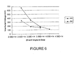
- FIG. 6 A graph of the interfacial voltage (V f ) at the substrate/buffer region interface versus 25keV implant dose is shown in Figure 6 .
- sample 4H and 6H silicon carbide wafers having a net concentration of nitrogen dopants of between 3.3E17 and 2.1E18 cm -3 were employed.
- a 50 nm thick PECVD silicon dioxide layer was formed on the surface of the wafers, and the wafers were implanted with various controlled doses of nitrogen at energy levels of 25keV and 50 keV respectively.
- the implant doses and energy levels for each wafer are shown in Table 1.
- the interfacial voltage i.e., the voltage drop attributable to the substrate/buffer interface
- the average values are plotted against the 25 keV implant dose in Figure 6 . As shown in Figure 6 , the interfacial voltage of the substrate/buffer interface decreases with increasing dosage.
Landscapes
- Chemical & Material Sciences (AREA)
- Engineering & Computer Science (AREA)
- Crystallography & Structural Chemistry (AREA)
- Materials Engineering (AREA)
- Metallurgy (AREA)
- Organic Chemistry (AREA)
- Inorganic Chemistry (AREA)
- Physics & Mathematics (AREA)
- Condensed Matter Physics & Semiconductors (AREA)
- General Physics & Mathematics (AREA)
- Manufacturing & Machinery (AREA)
- Computer Hardware Design (AREA)
- Microelectronics & Electronic Packaging (AREA)
- Power Engineering (AREA)
- Led Devices (AREA)
- Crystals, And After-Treatments Of Crystals (AREA)
- Physical Vapour Deposition (AREA)
- Electrodes Of Semiconductors (AREA)
Applications Claiming Priority (3)
| Application Number | Priority Date | Filing Date | Title |
|---|---|---|---|
| US35503402P | 2002-02-08 | 2002-02-08 | |
| US355034P | 2002-02-08 | ||
| PCT/US2003/003602 WO2003067637A2 (en) | 2002-02-08 | 2003-02-07 | Methods of treating a silicon carbide substrate for improved epitaxial deposition |
Publications (2)
| Publication Number | Publication Date |
|---|---|
| EP1488450A2 EP1488450A2 (en) | 2004-12-22 |
| EP1488450B1 true EP1488450B1 (en) | 2015-04-08 |
Family
ID=27734454
Family Applications (1)
| Application Number | Title | Priority Date | Filing Date |
|---|---|---|---|
| EP03737679.5A Expired - Lifetime EP1488450B1 (en) | 2002-02-08 | 2003-02-07 | Methods of treating a silicon carbide substrate for improved epitaxial deposition and resulting structures and devices |
Country Status (7)
Cited By (1)
| Publication number | Priority date | Publication date | Assignee | Title |
|---|---|---|---|---|
| EP4324961A1 (en) * | 2022-08-17 | 2024-02-21 | SiCrystal GmbH | Method for producing a bulk sic single crystal with improved quality using a sic seed crystal with a temporary protective oxide layer, and sic seed crystal with protective oxide layer |
Families Citing this family (6)
| Publication number | Priority date | Publication date | Assignee | Title |
|---|---|---|---|---|
| CN101673673B (zh) * | 2009-09-22 | 2013-02-27 | 上海宏力半导体制造有限公司 | 外延片形成方法及使用该方法形成的外延片 |
| JP5717674B2 (ja) * | 2012-03-02 | 2015-05-13 | 株式会社東芝 | 半導体装置の製造方法 |
| KR101926694B1 (ko) * | 2012-05-30 | 2018-12-07 | 엘지이노텍 주식회사 | 탄화규소 에피 웨이퍼 및 이의 제조 방법 |
| DE102016107557A1 (de) * | 2016-04-22 | 2017-10-26 | Nexwafe Gmbh | Siliziumwafer für ein elektronisches Bauelement und Verfahren zu dessen Herstellung |
| CN110006727A (zh) * | 2019-04-10 | 2019-07-12 | 深圳市锐骏半导体股份有限公司 | 一种离子注入机稳定性的监控方法 |
| CN112522781B (zh) * | 2021-02-18 | 2021-04-23 | 中芯集成电路制造(绍兴)有限公司 | 碳化硅衬底上的缓冲层及其形成方法 |
Family Cites Families (20)
| Publication number | Priority date | Publication date | Assignee | Title |
|---|---|---|---|---|
| JPS63104324A (ja) * | 1986-10-20 | 1988-05-09 | Fujitsu Ltd | 半導体結晶の成長方法 |
| JPH02240988A (ja) * | 1989-03-15 | 1990-09-25 | Hitachi Ltd | 半導体レーザ |
| JPH07326793A (ja) * | 1994-05-31 | 1995-12-12 | Showa Denko Kk | 化合物半導体発光ダイオード |
| US5523589A (en) * | 1994-09-20 | 1996-06-04 | Cree Research, Inc. | Vertical geometry light emitting diode with group III nitride active layer and extended lifetime |
| JPH08222812A (ja) * | 1995-02-17 | 1996-08-30 | Matsushita Electric Ind Co Ltd | 窒化ガリウム系化合物半導体の結晶成長方法 |
| JPH08288500A (ja) * | 1995-04-20 | 1996-11-01 | Hitachi Ltd | 炭化珪素半導体素子とその製造法及び用途 |
| JPH098353A (ja) * | 1995-06-14 | 1997-01-10 | Hitachi Cable Ltd | エピタキシャルウェハ及びその製造方法並びに発光ダイオード |
| US6201262B1 (en) * | 1997-10-07 | 2001-03-13 | Cree, Inc. | Group III nitride photonic devices on silicon carbide substrates with conductive buffer interlay structure |
| JP4166885B2 (ja) * | 1998-05-18 | 2008-10-15 | 富士通株式会社 | 光半導体装置およびその製造方法 |
| JP3956487B2 (ja) * | 1998-06-22 | 2007-08-08 | 富士電機デバイステクノロジー株式会社 | 炭化けい素半導体素子の製造方法 |
| US6459100B1 (en) * | 1998-09-16 | 2002-10-01 | Cree, Inc. | Vertical geometry ingan LED |
| US6329088B1 (en) * | 1999-06-24 | 2001-12-11 | Advanced Technology Materials, Inc. | Silicon carbide epitaxial layers grown on substrates offcut towards <1{overscore (1)}00> |
| DE19944144C2 (de) * | 1999-09-15 | 2001-07-26 | Rossendorf Forschzent | Verfahren zur Herstellung von vergrabenen Kontakten und Leitbahnen in kristallinen Siliziumkarbid-Halbleitersubstraten |
| JP2001237248A (ja) * | 2000-02-21 | 2001-08-31 | Mitsubishi Heavy Ind Ltd | 半導体装置及びその製造方法 |
| JP3889910B2 (ja) * | 2000-03-10 | 2007-03-07 | 三菱化学株式会社 | 半導体発光装置およびその製造方法 |
| JP4403629B2 (ja) * | 2000-04-06 | 2010-01-27 | 株式会社デンソー | 半導体発光装置 |
| JP2001332508A (ja) * | 2000-05-23 | 2001-11-30 | Matsushita Electric Ind Co Ltd | 半導体素子の製造方法 |
| JP2002016013A (ja) * | 2000-06-27 | 2002-01-18 | Nissan Motor Co Ltd | 炭化珪素半導体装置の製造方法 |
| KR100522758B1 (ko) * | 2000-06-28 | 2005-10-21 | 주식회사 하이닉스반도체 | 반도체 소자의 제조 방법 |
| JP2002223040A (ja) * | 2001-01-29 | 2002-08-09 | Ricoh Co Ltd | 半導体発光素子 |
-
2003
- 2003-02-07 AU AU2003210882A patent/AU2003210882A1/en not_active Abandoned
- 2003-02-07 CN CN201110068455.3A patent/CN102163664B/zh not_active Expired - Lifetime
- 2003-02-07 JP JP2003566885A patent/JP4846981B2/ja not_active Expired - Lifetime
- 2003-02-07 WO PCT/US2003/003602 patent/WO2003067637A2/en active Application Filing
- 2003-02-07 CN CN038034689A patent/CN1628370B/zh not_active Expired - Lifetime
- 2003-02-07 CA CA002474883A patent/CA2474883A1/en not_active Abandoned
- 2003-02-07 EP EP03737679.5A patent/EP1488450B1/en not_active Expired - Lifetime
- 2003-02-07 KR KR10-2004-7012250A patent/KR20040093712A/ko not_active Withdrawn
-
2010
- 2010-01-04 JP JP2010000117A patent/JP5528120B2/ja not_active Expired - Lifetime
Cited By (2)
| Publication number | Priority date | Publication date | Assignee | Title |
|---|---|---|---|---|
| EP4324961A1 (en) * | 2022-08-17 | 2024-02-21 | SiCrystal GmbH | Method for producing a bulk sic single crystal with improved quality using a sic seed crystal with a temporary protective oxide layer, and sic seed crystal with protective oxide layer |
| WO2024037747A1 (en) * | 2022-08-17 | 2024-02-22 | Sicrystal Gmbh | Method for producing a bulk sic single crystal with improved quality using a sic seed crystal with a temporary protective oxide layer, and sic seed crystal with protective oxide layer |
Also Published As
| Publication number | Publication date |
|---|---|
| WO2003067637A2 (en) | 2003-08-14 |
| JP5528120B2 (ja) | 2014-06-25 |
| JP2005517296A (ja) | 2005-06-09 |
| WO2003067637A3 (en) | 2004-01-15 |
| EP1488450A2 (en) | 2004-12-22 |
| JP4846981B2 (ja) | 2011-12-28 |
| CN102163664A (zh) | 2011-08-24 |
| KR20040093712A (ko) | 2004-11-08 |
| AU2003210882A1 (en) | 2003-09-02 |
| CN1628370B (zh) | 2011-05-18 |
| CN1628370A (zh) | 2005-06-15 |
| JP2010118672A (ja) | 2010-05-27 |
| CA2474883A1 (en) | 2003-08-14 |
| AU2003210882A8 (en) | 2003-09-02 |
| CN102163664B (zh) | 2014-07-23 |
Similar Documents
| Publication | Publication Date | Title |
|---|---|---|
| US6995398B2 (en) | Methods of treating a silicon carbide substrate for improved epitaxial deposition and resulting structures and devices | |
| CN1579008B (zh) | 用于垂直器件的背部欧姆触点的低温形成方法 | |
| EP1873817B1 (en) | Substrate having thin film of GaN joined thereon and method of fabricating the same | |
| EP1267422B1 (en) | Nitride semiconductor device and method for manufacturing the same | |
| US5432808A (en) | Compound semicondutor light-emitting device | |
| JP2008205514A (ja) | Iii−v族窒化物半導体素子 | |
| JP5528120B2 (ja) | 改良エピタキシャル堆積のために炭化珪素基板を処理する方法、及びその方法によって得られる構造とデバイス | |
| EP3001465B1 (en) | Light-emitting element and method for preparing same | |
| EP2154709A2 (en) | Method of manufacturing group III nitride semiconductor layer bonded substrate | |
| US20240071756A1 (en) | Method for manufacturing group iii nitride semiconductor substrate | |
| EP3157068B1 (en) | Semiconductor multilayer structure and method for producing same | |
| WO2005022655A1 (en) | Algainn based optical device and fabrication method thereof | |
| CN218677183U (zh) | 一种多量子阱结构 | |
| KR20050035325A (ko) | 질화물 반도체 발광소자 및 그 제조방법 | |
| JP2003124515A (ja) | 窒化物系化合物半導体の製造方法及び半導体素子 | |
| KR100576850B1 (ko) | 질화물 반도체 발광소자 제조방법 | |
| KR20160141492A (ko) | 발광 다이오드 및 그 제조 방법 | |
| KR100348280B1 (ko) | 청색 발광 소자 제조방법 | |
| KR20010019357A (ko) | 질화물 반도체 발광소자 | |
| JP2010177281A (ja) | 窒化ガリウム系化合物半導体基板及びその製造方法、並びに半導体素子 | |
| JP2006310714A (ja) | 窒化物半導体素子および窒化物半導体素子の製造方法 |
Legal Events
| Date | Code | Title | Description |
|---|---|---|---|
| PUAI | Public reference made under article 153(3) epc to a published international application that has entered the european phase |
Free format text: ORIGINAL CODE: 0009012 |
|
| 17P | Request for examination filed |
Effective date: 20040820 |
|
| AK | Designated contracting states |
Kind code of ref document: A2 Designated state(s): AT BE BG CH CY CZ DE DK EE ES FI FR GB GR HU IE IT LI LU MC NL PT SE SI SK TR |
|
| AX | Request for extension of the european patent |
Extension state: AL LT LV MK RO |
|
| 17Q | First examination report despatched |
Effective date: 20071022 |
|
| REG | Reference to a national code |
Ref country code: DE Ref legal event code: R079 Ref document number: 60347485 Country of ref document: DE Free format text: PREVIOUS MAIN CLASS: H01L0021040000 Ipc: C30B0031000000 |
|
| GRAP | Despatch of communication of intention to grant a patent |
Free format text: ORIGINAL CODE: EPIDOSNIGR1 |
|
| RIC1 | Information provided on ipc code assigned before grant |
Ipc: C30B 33/00 20060101ALI20140924BHEP Ipc: H01L 21/04 20060101ALI20140924BHEP Ipc: H01L 33/00 20100101ALI20140924BHEP Ipc: C30B 31/00 20060101AFI20140924BHEP |
|
| INTG | Intention to grant announced |
Effective date: 20141024 |
|
| GRAS | Grant fee paid |
Free format text: ORIGINAL CODE: EPIDOSNIGR3 |
|
| GRAA | (expected) grant |
Free format text: ORIGINAL CODE: 0009210 |
|
| AK | Designated contracting states |
Kind code of ref document: B1 Designated state(s): AT BE BG CH CY CZ DE DK EE ES FI FR GB GR HU IE IT LI LU MC NL PT SE SI SK TR |
|
| REG | Reference to a national code |
Ref country code: GB Ref legal event code: FG4D |
|
| REG | Reference to a national code |
Ref country code: CH Ref legal event code: EP |
|
| REG | Reference to a national code |
Ref country code: IE Ref legal event code: FG4D |
|
| REG | Reference to a national code |
Ref country code: AT Ref legal event code: REF Ref document number: 720665 Country of ref document: AT Kind code of ref document: T Effective date: 20150515 |
|
| REG | Reference to a national code |
Ref country code: DE Ref legal event code: R096 Ref document number: 60347485 Country of ref document: DE Effective date: 20150521 |
|
| REG | Reference to a national code |
Ref country code: AT Ref legal event code: MK05 Ref document number: 720665 Country of ref document: AT Kind code of ref document: T Effective date: 20150408 |
|
| REG | Reference to a national code |
Ref country code: NL Ref legal event code: VDEP Effective date: 20150408 |
|
| PG25 | Lapsed in a contracting state [announced via postgrant information from national office to epo] |
Ref country code: NL Free format text: LAPSE BECAUSE OF FAILURE TO SUBMIT A TRANSLATION OF THE DESCRIPTION OR TO PAY THE FEE WITHIN THE PRESCRIBED TIME-LIMIT Effective date: 20150408 |
|
| PG25 | Lapsed in a contracting state [announced via postgrant information from national office to epo] |
Ref country code: PT Free format text: LAPSE BECAUSE OF FAILURE TO SUBMIT A TRANSLATION OF THE DESCRIPTION OR TO PAY THE FEE WITHIN THE PRESCRIBED TIME-LIMIT Effective date: 20150810 Ref country code: ES Free format text: LAPSE BECAUSE OF FAILURE TO SUBMIT A TRANSLATION OF THE DESCRIPTION OR TO PAY THE FEE WITHIN THE PRESCRIBED TIME-LIMIT Effective date: 20150408 Ref country code: FI Free format text: LAPSE BECAUSE OF FAILURE TO SUBMIT A TRANSLATION OF THE DESCRIPTION OR TO PAY THE FEE WITHIN THE PRESCRIBED TIME-LIMIT Effective date: 20150408 |
|
| PG25 | Lapsed in a contracting state [announced via postgrant information from national office to epo] |
Ref country code: GR Free format text: LAPSE BECAUSE OF FAILURE TO SUBMIT A TRANSLATION OF THE DESCRIPTION OR TO PAY THE FEE WITHIN THE PRESCRIBED TIME-LIMIT Effective date: 20150709 Ref country code: AT Free format text: LAPSE BECAUSE OF FAILURE TO SUBMIT A TRANSLATION OF THE DESCRIPTION OR TO PAY THE FEE WITHIN THE PRESCRIBED TIME-LIMIT Effective date: 20150408 |
|
| REG | Reference to a national code |
Ref country code: DE Ref legal event code: R097 Ref document number: 60347485 Country of ref document: DE |
|
| PG25 | Lapsed in a contracting state [announced via postgrant information from national office to epo] |
Ref country code: EE Free format text: LAPSE BECAUSE OF FAILURE TO SUBMIT A TRANSLATION OF THE DESCRIPTION OR TO PAY THE FEE WITHIN THE PRESCRIBED TIME-LIMIT Effective date: 20150408 Ref country code: DK Free format text: LAPSE BECAUSE OF FAILURE TO SUBMIT A TRANSLATION OF THE DESCRIPTION OR TO PAY THE FEE WITHIN THE PRESCRIBED TIME-LIMIT Effective date: 20150408 |
|
| PLBE | No opposition filed within time limit |
Free format text: ORIGINAL CODE: 0009261 |
|
| STAA | Information on the status of an ep patent application or granted ep patent |
Free format text: STATUS: NO OPPOSITION FILED WITHIN TIME LIMIT |
|
| PG25 | Lapsed in a contracting state [announced via postgrant information from national office to epo] |
Ref country code: SK Free format text: LAPSE BECAUSE OF FAILURE TO SUBMIT A TRANSLATION OF THE DESCRIPTION OR TO PAY THE FEE WITHIN THE PRESCRIBED TIME-LIMIT Effective date: 20150408 Ref country code: CZ Free format text: LAPSE BECAUSE OF FAILURE TO SUBMIT A TRANSLATION OF THE DESCRIPTION OR TO PAY THE FEE WITHIN THE PRESCRIBED TIME-LIMIT Effective date: 20150408 |
|
| 26N | No opposition filed |
Effective date: 20160111 |
|
| PG25 | Lapsed in a contracting state [announced via postgrant information from national office to epo] |
Ref country code: IT Free format text: LAPSE BECAUSE OF FAILURE TO SUBMIT A TRANSLATION OF THE DESCRIPTION OR TO PAY THE FEE WITHIN THE PRESCRIBED TIME-LIMIT Effective date: 20150408 |
|
| PG25 | Lapsed in a contracting state [announced via postgrant information from national office to epo] |
Ref country code: BE Free format text: LAPSE BECAUSE OF NON-PAYMENT OF DUE FEES Effective date: 20160229 Ref country code: SI Free format text: LAPSE BECAUSE OF FAILURE TO SUBMIT A TRANSLATION OF THE DESCRIPTION OR TO PAY THE FEE WITHIN THE PRESCRIBED TIME-LIMIT Effective date: 20150408 |
|
| PG25 | Lapsed in a contracting state [announced via postgrant information from national office to epo] |
Ref country code: BE Free format text: LAPSE BECAUSE OF FAILURE TO SUBMIT A TRANSLATION OF THE DESCRIPTION OR TO PAY THE FEE WITHIN THE PRESCRIBED TIME-LIMIT Effective date: 20150408 |
|
| PG25 | Lapsed in a contracting state [announced via postgrant information from national office to epo] |
Ref country code: LU Free format text: LAPSE BECAUSE OF FAILURE TO SUBMIT A TRANSLATION OF THE DESCRIPTION OR TO PAY THE FEE WITHIN THE PRESCRIBED TIME-LIMIT Effective date: 20160207 Ref country code: MC Free format text: LAPSE BECAUSE OF FAILURE TO SUBMIT A TRANSLATION OF THE DESCRIPTION OR TO PAY THE FEE WITHIN THE PRESCRIBED TIME-LIMIT Effective date: 20150408 |
|
| REG | Reference to a national code |
Ref country code: CH Ref legal event code: PL |
|
| GBPC | Gb: european patent ceased through non-payment of renewal fee |
Effective date: 20160207 |
|
| PG25 | Lapsed in a contracting state [announced via postgrant information from national office to epo] |
Ref country code: LI Free format text: LAPSE BECAUSE OF NON-PAYMENT OF DUE FEES Effective date: 20160229 Ref country code: CH Free format text: LAPSE BECAUSE OF NON-PAYMENT OF DUE FEES Effective date: 20160229 |
|
| REG | Reference to a national code |
Ref country code: FR Ref legal event code: ST Effective date: 20161028 |
|
| REG | Reference to a national code |
Ref country code: IE Ref legal event code: MM4A |
|
| PG25 | Lapsed in a contracting state [announced via postgrant information from national office to epo] |
Ref country code: IE Free format text: LAPSE BECAUSE OF NON-PAYMENT OF DUE FEES Effective date: 20160207 Ref country code: GB Free format text: LAPSE BECAUSE OF NON-PAYMENT OF DUE FEES Effective date: 20160207 Ref country code: FR Free format text: LAPSE BECAUSE OF NON-PAYMENT OF DUE FEES Effective date: 20160229 |
|
| PG25 | Lapsed in a contracting state [announced via postgrant information from national office to epo] |
Ref country code: SE Free format text: LAPSE BECAUSE OF FAILURE TO SUBMIT A TRANSLATION OF THE DESCRIPTION OR TO PAY THE FEE WITHIN THE PRESCRIBED TIME-LIMIT Effective date: 20150408 |
|
| PG25 | Lapsed in a contracting state [announced via postgrant information from national office to epo] |
Ref country code: HU Free format text: LAPSE BECAUSE OF FAILURE TO SUBMIT A TRANSLATION OF THE DESCRIPTION OR TO PAY THE FEE WITHIN THE PRESCRIBED TIME-LIMIT; INVALID AB INITIO Effective date: 20030207 Ref country code: CY Free format text: LAPSE BECAUSE OF FAILURE TO SUBMIT A TRANSLATION OF THE DESCRIPTION OR TO PAY THE FEE WITHIN THE PRESCRIBED TIME-LIMIT Effective date: 20150408 |
|
| PG25 | Lapsed in a contracting state [announced via postgrant information from national office to epo] |
Ref country code: TR Free format text: LAPSE BECAUSE OF FAILURE TO SUBMIT A TRANSLATION OF THE DESCRIPTION OR TO PAY THE FEE WITHIN THE PRESCRIBED TIME-LIMIT Effective date: 20150408 |
|
| PG25 | Lapsed in a contracting state [announced via postgrant information from national office to epo] |
Ref country code: BG Free format text: LAPSE BECAUSE OF FAILURE TO SUBMIT A TRANSLATION OF THE DESCRIPTION OR TO PAY THE FEE WITHIN THE PRESCRIBED TIME-LIMIT Effective date: 20150408 |
|
| PGFP | Annual fee paid to national office [announced via postgrant information from national office to epo] |
Ref country code: DE Payment date: 20220225 Year of fee payment: 20 |
|
| REG | Reference to a national code |
Ref country code: DE Ref legal event code: R071 Ref document number: 60347485 Country of ref document: DE |